
Features
l Suitable for coupling with blue scintillator (LSO, GSO, etc.)
l Internal quantum efficiency: 100 % (=420 nm)
l S3590-19: bare chip type (without window)
Applications
l Radiation detection (PET, etc.)
l X-ray detection
P H O T O D I O D E
Si PIN photodiode
Large area Si PIN photodiode for scintillation counting
S3590-18/-19
s
Absolute maximum ratings
Parameter
Symbol
Value
Unit
Reverse voltage
V
R
100
V
Power dissipation
P
100
mW
Operating temperature
Topr
-20 to +60
∞C
Storage temperature
Tstg
-20 to +80
∞C
s
Electrical and optical characteristics (Ta=25 ∞C)
S3590-18
S3590-19
Parameter
Symbol
Condition
Min.
Typ.
Max.
Min.
Typ.
Max.
Unit
Spectral response range
-
320 to
1100
-
-
320 to
1100
-nm
Peak sensitivity wavelength
p
-
960
-
-
960
-
nm
=p
-0.65
- -0.58
- A/W
=420 nm (LSO)
-0.28
- -0.33
- A/W
=480 nm (BGO)
-0.34
- -0.37
- A/W
Photo sensitivity
S
=540 nm (CsI)
-0.38
- - 0.4
- A/W
Short circuit current
Isc
100 lx
-
100
-
-
86
-
µA
Dark current
I
D
V
R
=70 V
-
4
10
-
4
10
nA
Temperature coefficient of I
,
T
CID
-
1.12
-
-
1.12
-
times/∞C
Cut-off frequency
fc
V
R
=70 V, -3 dB
R
L
=50
-40
- -40
-MHz
Terminal capacitance
Ct
V
R
=70 V, f=1 MHz
-
40
-
-
40
-
pF
Noise equivalent power
NEP
-
7.6 ◊ 10
-14
-
-
7.6 ◊ 10
-14
-W/Hz
1/2
HAMAMATSU PHOTONICS K.K., Solid State Division
1126-1 Ichino-cho, Hamamatsu City, 435-8558 Japan, Telephone: (81) 053-434-3311, Fax: (81) 053-434-5184, http://www.hamamatsu.com
U.S.A.: Hamamatsu Corporation: 360 Foothill Road, P.O.Box 6910, Bridgewater, N.J. 08807-0910, U.S.A., Telephone: (1) 908-231-0960, Fax: (1) 908-231-1218
Germany: Hamamatsu Photonics Deutschland GmbH: Arzbergerstr. 10, D-82211 Herrsching am Ammersee, Germany, Telephone: (49) 08152-3750, Fax: (49) 08152-2658
France: Hamamatsu Photonics France S.A.R.L.: 8, Rue du Saule Trapu, Parc du Moulin de Massy, 91882 Massy Cedex, France, Telephone: 33-(1) 69 53 71 00, Fax: 33-(1) 69 53 71 10
United Kingdom: Hamamatsu Photonics UK Limited: 2 Howard Court, 10 Tewin Road, Welwyn Garden City, Hertfordshire AL7 1BW, United Kingdom, Telephone: (44) 1707-294888, Fax: (44) 1707-325777
North Europe: Hamamatsu Photonics Norden AB: Smidesv‰gen 12, SE-171 41 Solna, Sweden, Telephone: (46) 8-509-031-00, Fax: (46) 8-509-031-01
Italy: Hamamatsu Photonics Italia S.R.L.: Strada della Moia, 1/E, 20020 Arese, (Milano), Italy, Telephone: (39) 02-935-81-733, Fax: (39) 02-935-81-741
Information furnished by HAMAMATSU is believed to be reliable. However, no responsibility is assumed for possible inaccuracies or omissions.
Specifications are subject to change without notice. No patent rights are granted to any of the circuits described herein. ©2001 Hamamatsu Photonics K.K.
Si PIN photodiode
S3590-18/-19
Cat. No. KPIN1039E01
Mar. 2001 DN
REVERSE VOLTAGE (V)
(Typ. Ta=25 ∞C)
DARK CURRENT
1
0.1
100 pA
1 nA
100 nA
10 nA
10
100
REVERSE VOLTAGE (V)
(Typ. Ta=25 ∞C)
TERMINAL CAPACITANCE
1
0.1
10 pF
1 nF
100 pF
10
100
0.45
LEAD
PHOTOSENSITIVE
SURFACE
ACTIVE AREA
5.0 ± 0.2
1.25
10
1.78 ± 0.2
0.7
10.0
10.0
WHITE CERAMIC
14.5
1.4
12.7
+
0
-
0.5
+0
- 0.5
The coating resin may extend a
maximum of 0.1 mm beyond the
upper surface of the package.
WAVELENGTH (nm)
(Typ. Ta=25 ∞C)
PHOTO SENSITIVITY (A/W)
400
200
0
0.1
0.2
0.3
0.7
0.6
0.5
0.4
600
800
1000
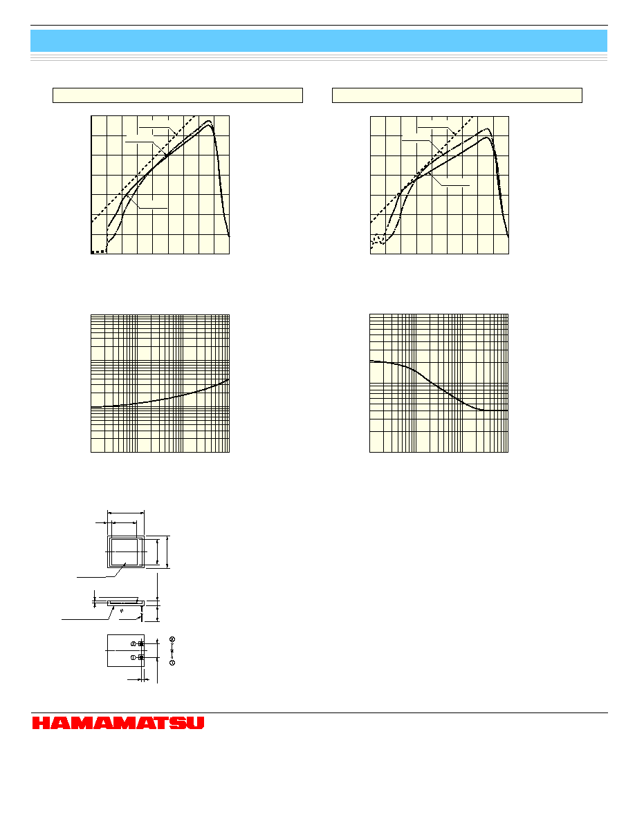
QE=100 %
S3590-08
S3590-18
s Spectral response
WAVELENGTH (nm)
(Typ. Ta=25 ∞C)
PHOTO SENSITIVITY (A/W)
400
200
0
0.1
0.2
0.3
0.7
0.6
0.5
0.4
600
800
1000
QE=100 %
S3590-09
S3590-19
s Dark current vs. reverse voltage
s Terminal capacitance vs. reverse voltage
KPINB0223EA
KPINB0224EA
KPINB0225EA
KPINB0226EA
S3590-18
S3590-19 (Bare chip type)
s
Dimensional outline (unit: mm)
KPINA0014ED