NMOS linear image sensors are self-scanning photodiode arrays designed specifically as detectors for multichannel spectroscopy. The scanning
circuit is made up of N-channel MOS transistors, has low power consumption and is easy to handle. Each photodiode has a large active area,
high UV sensitivity yet very low noise, delivering a high S/N even at low light levels. Current output type NMOS linear image sensors also offer
excellent output linearity and wide dynamic range.
S3901-FX series image sensors are variants of S3901-F series NMOS image sensors. Having a phosphor-coated fiber optic plate (FOP) as the
light input window, the S3901-FX series was developed for detection of X-rays and electrons. The S3901-FX offers particularly high sensitivity to
X-rays from 10 k to 100 keV. The phosphor material used is gadolinium ox sulfide (Gd
2
O
2
S ∑ Tb) whose composition is carefully selected to
provide optimum sensitivity and resolution with a peak emission at 550 nm wavelength.
The S3901-FX series active area consists of a photodiode array with pixels formed at 50 µm pitches and a height of 2.5 mm. The number of pixels
can be selected from 256 or 512.
Hamamatsu S3902/S3903/S3904 series NMOS linear image sensors are also available with FOP windows coated with the same phosphor
material as S3901-FX series.
Using photodiodes with no phosphor and FOP window also allows direct detection of X-rays at energy levels below 10 keV.
Features
l
Wide active area
Pixel pitch: 50 µm
Pixel height: 2.5 mm
l
Low dark current and high saturation charge allow a
long integration time and a wide dynamic range at room
temperature
l
Excellent output linearity and sensitivity spatial uniformity
l
Low power consumption: 1 mW Max.
l
Start pulse and clock pulse are CMOS logic compatible
Applications
l
Test equipment using X-ray and electron beam transmission
l
X-ray non-destructive inspection
l
X-ray and electron beam detector
I M A G E S E N S O R
NMOS linear image sensor
Image sensor highly sensitive to X-rays from 10 k to 100 keV
S3901-FX series
2.5 mm
1.0 µm
1.0 µm
400 µm
OXIDATION SILICON
N TYPE SILICON
P TYPE SILICON
FIBER OPTIC PLATE
45 µm
50 µm
PHOSPHOR MATERIAL
Vss
START
st
CLOCK
CLOCK
1
2
ACTIVE
PHOTODIODE
SATURATION
CONTROL GATE
SATURATION
CONTROL DRAIN
DUMMY DIODE
DUMMY VIDEO
ACTIVE VIDEO
END OF SCAN
DIGITAL SHIFT RESISTER
(MOS SHIFT RESISTER)
KMPDC0020EA
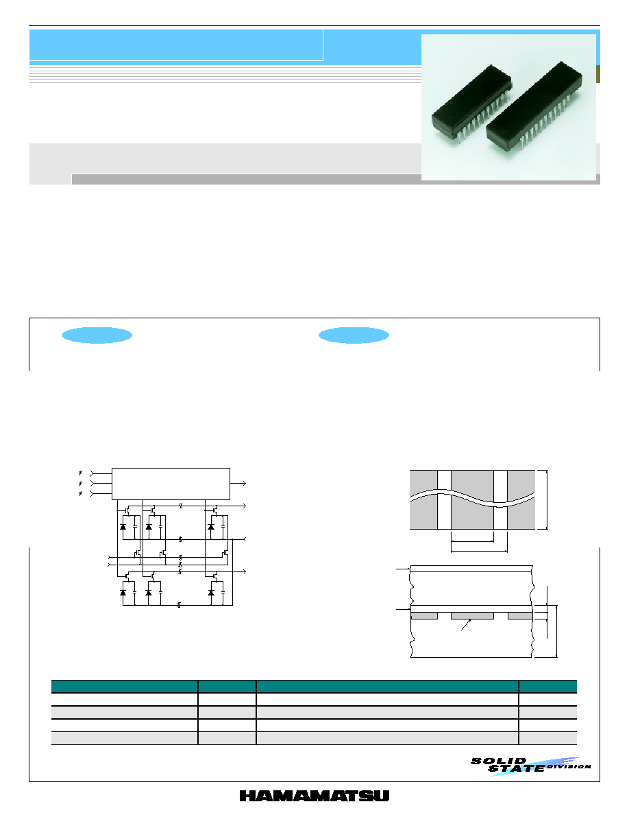
Figure 1 Equivalent circuit
Figure 2 Active area structure
s
Absolute maximum ratings
Parameter
Symbol
Value
Unit
Input pulse (1, 2, st) voltage
V
15
V
Power consumption *
1
P
1
mW
Operating temperature *
2
Topr
-30 to +60
∞C
Storage temperature
Tstg
-40 to +80
∞C
*1: V=5.0 V
*2: No condensation
KMPDC0008EA
NMOS linear image sensor
S3901-FX series
s
Shape specifications
Parameter
S3901-256FX
S3901-512FX
Unit
Number of pixels
256
512
-
Package length
31.75
40.6
mm
Number of pin
22
-
Window material *
3
Fiber optic plate
-
Weight
8.0
10.0
g
*3: To prevent unwanted effects from stray light, S3901-FX series is supplied with an aluminum cover fitted on the phosphor-
coated FOP.
s
Specifications (Ta=25 ∞C)
Parameter
Symbol
Min.
Typ.
Max.
Unit
Pixel pitch
-
-
50
-
µm
Pixel height
-
-
2.5
-
mm
Spectral response range (20 % of peak)
10 to 100
keV
Photo sensitivity
S
-
14
-
pC/mR
Photodiode dark current *
4
I
D
-
0.2
0.6
pA
Photodiode capacitance *
4
Cph
-
20
-
pF
Saturation exposure *
4
Esat
-
2.8
-
mR
Saturation output charge *
4
Qsat
-
50
-
pC
Photo response non-uniformity *
5
PRNU
-
-
±10
%
*4: Vb=2.0 V, V=5.0 V
*5: Measured under the following conditions including uniformity in the phosphor emission (but excluding dark current
components).
Tungsten cathode X-ray tube: 40 keV
Distance between S3901-FX series and X-ray tube: 30 cm
Phosphor material: Gd
2
O
2
S . Tb (thickness=200 µm, p=550 nm, decay time=1 ms)
s
Electrical characteristics (Ta=25 ∞C)
Parameter
Symbol
Condition
Min.
Typ.
Max.
Unit
High V1, V2 (H)
4.5
5
10
V
Clock pulse (1, 2) voltage
Low V1, V2 (L)
0
-
0.4
V
High
Vs (H)
4.5
V1
10
V
Start pulse (st) voltage
Low
Vs (L)
0
-
0.4
V
Video bias voltage *
6
Vb
1.5
V - 3.0
V - 2.5
V
Saturation control gate voltage
Vscg
-
0
-
V
Saturation control drain voltage
Vscd
-
Vb
-
V
Clock pulse (1, 2) rise / fall time *
7
tr1, tr2
tf1, tf2
-
20
-
ns
Clock pulse (1, 2) pulse width
tpw1, tpw2
200
-
-
ns
Start pulse (st) rise / fall time
trs, tfs
-
20
-
ns
Start pulse (st) pulse width
tpws
200
-
-
ns
Start pulse (st) and clock pulse
(2) overlap
tov
200
-
-
ns
Clock pulse space *
7
X
1
, X
2
trf - 20
-
-
ns
Data rate *
8
f
0.1
-
2000
kHz
-
120 (-256 FX)
-
ns
Video delay time
tvd
50 % of
saturation *
8,
*
9
-
160 (-512 FX)
-
ns
-
36 (-256 FX)
-
pF
Clock pulse (1, 2)
line capacitance
C
5 V bias
-
67 (-512 FX)
-
pF
-
20 (-256 FX)
-
pF
Saturation control gate (Vscg)
line capacitance
Cscg
5 V bias
-
35 (-512 FX)
-
pF
-
11 (-256 FX)
-
pF
Video line capacitance
C
V
2 V bias
-
20 (-512 FX)
-
pF
*6: V is input pulse voltage
*7: trf is the clock pulse rise or fall time. A clock pulse space of rise time/fall time - 20 ns (nanoseconds) or more should be input
if the clock pulse rise or fall time is longer than 20
ns.
*8: Vb=2.0 V, V=5.0 V
*9: Measured with C7883 driver circuit.
NMOS linear image sensor
S3901-FX series
HAMAMATSU PHOTONICS K.K., Solid State Division
1126-1 Ichino-cho, Hamamatsu City, 435-8558 Japan, Telephone: (81) 053-434-3311, Fax: (81) 053-434-5184, http://www.hamamatsu.com
U.S.A.: Hamamatsu Corporation: 360 Foothill Road, P.O.Box 6910, Bridgewater, N.J. 08807-0910, U.S.A., Telephone: (1) 908-231-0960, Fax: (1) 908-231-1218
Germany: Hamamatsu Photonics Deutschland GmbH: Arzbergerstr. 10, D-82211 Herrsching am Ammersee, Germany, Telephone: (49) 08152-3750, Fax: (49) 08152-2658
France: Hamamatsu Photonics France S.A.R.L.: 8, Rue du Saule Trapu, Parc du Moulin de Massy, 91882 Massy Cedex, France, Telephone: 33-(1) 69 53 71 00, Fax: 33-(1) 69 53 71 10
United Kingdom: Hamamatsu Photonics UK Limited: 2 Howard Court, 10 Tewin Road, Welwyn Garden City, Hertfordshire AL7 1BW, United Kingdom, Telephone: (44) 1707-294888, Fax: (44) 1707-325777
North Europe: Hamamatsu Photonics Norden AB: Smidesv‰gen 12, SE-171 41 Solna, Sweden, Telephone: (46) 8-509-031-00, Fax: (46) 8-509-031-01
Italy: Hamamatsu Photonics Italia S.R.L.: Strada della Moia, 1/E, 20020 Arese, (Milano), Italy, Telephone: (39) 02-935-81-733, Fax: (39) 02-935-81-741
Information furnished by HAMAMATSU is believed to be reliable. However, no responsibility is assumed for possible inaccuracies or omissions.
Specifications are subject to change without notice. No patent rights are granted to any of the circuits described herein. ©2001 Hamamatsu Photonics K.K.
Cat. No. KMPD1005E04
Apr. 2001 DN
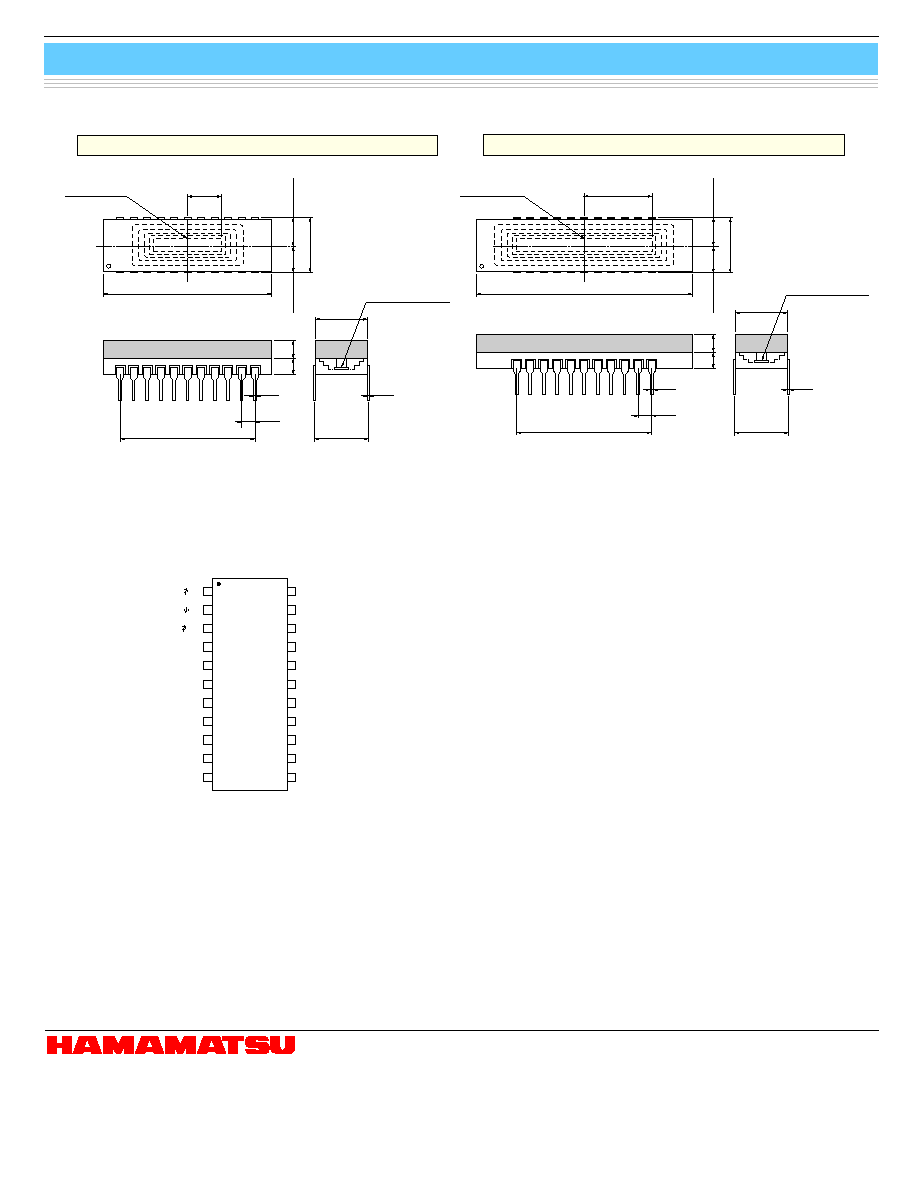
Figure 3 Dimensional outlines (unit: mm)
S3901-256FX
0.51
25.4
2.54
3.0
3.4
ACTIVE AREA
12.8 ◊ 2.5
6.4 ± 0.3
31.75
10.4
5.4 ± 0.2
5.0 ± 0.2
0.25
10.0
10.16
PHOTOSENSITIVE
SURFACE
KMPDA0031EA
S3901-512FX
0.51
25.4
40.6
10.4
5.4 ± 0.2
5.0 ± 0.2
12.8 ± 0.3
ACTIVE AREA
25.6 ◊ 2.5
0.25
10.16
2.54
10.0
3.0
3.4
PHOTOSENSITIVE
SURFACE
KMPDA0032EA
NC
NC
NC
NC
NC
NC
NC
NC
NC
NC
END OF SCAN
1
2
3
4
5
6
7
8
9
10
11
22
21
20
19
18
17
16
15
14
13
12
2
1
st
Vss
Vscg
NC
Vscd
Vss
ACTIVE VIDEO
DUMMY VIDEO
Vsub
Vss, Vsub and NC should be grounded.
KMPDC0056EA
Figure 4 Pin connection