NMOS linear image sensors are self-scanning photodiode arrays designed specifically as detectors for multichannel spectroscopy. The scanning
circuit is made up of N-channel MOS transistors, operates at low power consumption and is easy to handle. Each photodiode has a large active
area, high UV sensitivity yet very low noise, delivering a high S/N even at low light levels. The current output type NMOS linear image sensors
also feature excellent output linearity and wide dynamic range. S3901-1024Q uses photodiodes with a height of 2.5 mm, arrayed at a spacing of
50 µm. S3904-2048Q has photodiodes with a height of 2.5 mm, arrayed at a spacing of 25 µm. The photodiode arrays are available in 2 different
pixel quantities, 1024 (S3901-1024Q) and 2048 (S3904-2048Q). Quartz glass is the standard window material. Dedicated driver circuit C7615
(sold separately) is also provided.
Features
l
Large active area, long detection length
Pixel pitch: 50 µm (S3901-1024Q)
25 µm (S3904-2048Q)
Pixel height: 2.5 mm
Active area length: 51.2 mm
l
High UV sensitivity with good stability
l
Low dark current and large saturation charge allow long
integration time and a wide dynamic range at room temperature
l
Excellent output linearity and sensitivity spatial uniformity
l
Low power consumption: 1 mW Max.
l
Start pulse and clock pulses are CMOS logic compatible
Applications
l
Multichannel spectrophotometry
l
Image readout system
I M A G E S E N S O R
NMOS linear image sensor
Large active area type with 51.2 mm detection length
S3901-1024Q, S3904-2048Q
c
1.0 µm
1.0 µm
400 µm
OXIDATION SILICON
N TYPE SILICON
P TYPE SILICON
S3901-1024Q: a=50 µm, b=45 µm, c=2.5 mm
S3904-2048Q: a=25 µm, b=20 µm, c=2.5 mm
b
a
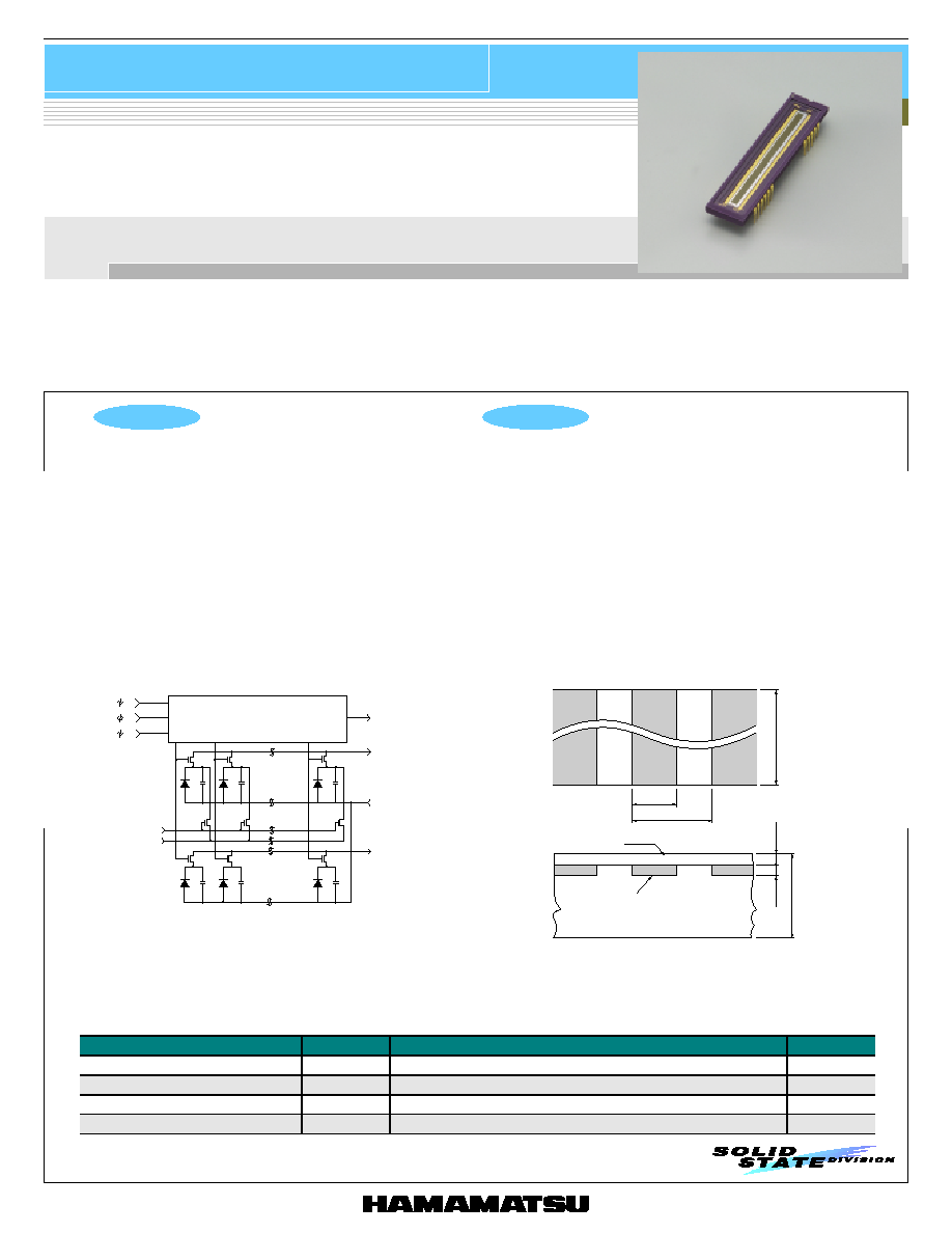
Vss
START
st
CLOCK
CLOCK
1
2
ACTIVE
PHOTODIODE
SATURATION
CONTROL GATE
SATURATION
CONTROL DRAIN
DUMMY DIODE
DUMMY VIDEO
ACTIVE VIDEO
END OF SCAN
DIGITAL SHIFT RESISTER
(MOS SHIFT RESISTER)
KMPDC0020EA
Figure 1 Equivalent circuit
Figure 2 Active area structure
s Absolute maximum ratings
Parameter
Symbol
Value
Unit
Input pulse (
1,
2,
st) voltage
V
15
V
Power consumption *
1
P
1
mW
Operating temperature *
2
Topr
-40 to +65
∞C
Storage temperature
Tstg
-40 to +85
∞C
*1: V
=5.0 V
*2: No condensation
KMPDA0124EB
1
NMOS linear image sensor
S3901-1024Q, S3904-2048Q
s Shape specifications
Parameter
S3901-1024Q
S3904-2048Q
Unit
Number of pixels
1024
2048
-
Package length
65.0
mm
Number of pin
22
-
Window material *
3
Quartz
-
Weight
8.5
g
*3: Fiber optic plate is available.
s Specifications (Ta=25 ∞C)
S3901-1024Q
S3904-2048Q
Parameter
Symbol
Min.
Typ.
Max.
Min.
Typ.
Max.
Unit
Pixel pitch
-
-
50
-
-
25
-
µm
Pixel height
-
-
2.5
-
-
2.5
-
mm
Spectral response range
(10 % of peak)
200 to 1000
200 to 1000
nm
Peak sensitivity wavelength
p
-
600
-
-
600
-
nm
Photodiode dark current *
4
I
D
-
0.2
0.6
-
0.1
0.3
pA
Photodiode capacitance *
4
Cph
-
20
-
-
10
-
pF
Saturation exposure *
4,
*
5
Esat
-
180
-
-
180
-
mlx ∑ s
Saturation output charge *
4
Qsat
-
50
-
-
25
-
pC
Photo response non-uniformity *
6
PRNU
-
-
±3
-
-
±3
%
*4: Vb=2.0 V, V
=5.0 V
*5: 2856 K, tungsten lamp
*6: 50 % of saturation, excluding the start pixel and last pixel
s Electrical characteristics (Ta=25 ∞C)
S3901-1024Q
S3904-2048Q
Parameter
Symbol
Condition
Min.
Typ.
Max.
Min.
Typ.
Max.
Unit
High V
1, V
2 (H)
4.5
5
10
4.5
5
10
V
Clock pulse (
1,
2)
voltage
Low
V
1, V
2 (L)
0
-
0.4
0
-
0.4
V
High
V
s (H)
4.5
V
1
10
4.5
V
1
10
V
Start pulse (
st) voltage
Low
V
s (L)
0
-
0.4
0
-
0.4
V
Video bias voltage *
7
Vb
1.5
V
- 3.0
V
- 2.5
1.5
V
- 3.0
V
- 2.5
V
Saturation control gate voltage
Vscg
-
0
-
-
0
-
V
Saturation control drain voltage
Vscd
-
Vb
-
-
Vb
-
V
Cl ock puls e (
1,
2) rise/fall ti me *
8
tr
1, tr
2
tf
1, tf
2
-
20
-
-
20
-
ns
Clock pulse (
1,
2) pulse width
tpw
1, tpw
2
200
-
-
200
-
-
ns
Start pulse (
st) rise/fall time
tr
s, tf
s
-
20
-
-
20
-
ns
Start pulse (
st) pulse width
tpw
s
200
-
-
200
-
-
ns
Start pulse (
st) and clock pulse
(
2) overlap
t
ov
200
-
-
200
-
-
ns
Clock pulse space *
8
X
1
, X
2
trf - 20
-
-
trf - 20
-
-
ns
Data rate *
9
f
0.1
-
2000
0.1
-
2000
kHz
Video delay time
tvd
50 % of
saturation
*
9,
*
1 0
-
200
-
-
250
-
ns
Clock pulse (
1,
2)
line capacitance
C
5 V bias
-
134
-
-
200
-
pF
Saturation control gate (Vscg)
line capacitance
Cscg
5 V bias
-
63
-
-
87
-
pF
Video line capacitance
C
V
2 V bias
-
45
-
-
60
-
pF
*7: V
is input pulse voltage (refer to figure 8) .
*8: trf is the clock pulse rise or fall time. A clock pulse space of
"rise time/fall time - 20
" ns (nanoseconds) or more should be
input if the clock pulse rise or fall time is longer than 20
ns (refer to figure 7) .
*9: Vb=2.0 V, V
=5.0 V
*10: Measured with C7883 driver circuit.
2
NMOS linear image sensor
S3901-1024Q, S3904-2048Q
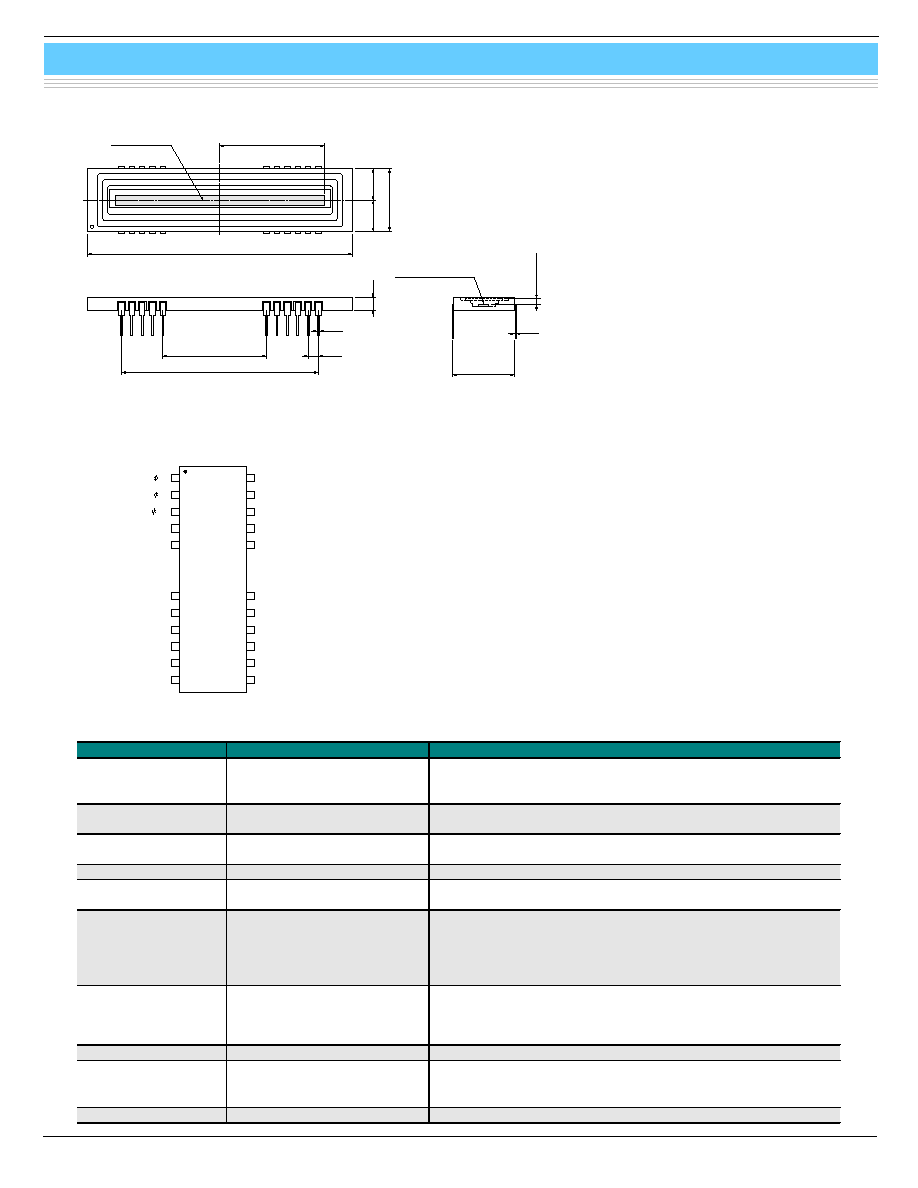
Figure 3 Dimensional outline (unit: mm)
KMPDC0109EA
Figure 4 Pin connection
KMPDA0123EA
25.6 ± 0.5
7.75 ± 0.2
7.75 ± 0.2
15.5
65.0
0.25
15.24
1.3 ± 0.2 *
3.0
PHOTOSENSITIVE
SURFACE
* Optical distance from the outer surface
of the quartz window to the chip surface
2.54
0.46
25.4
48.26
ACTIVE AREA
51.2 ◊ 2.5
NC
NC
NC
NC
NC
NC
NC
NC
NC
NC
END OF SCAN
1
2
3
4
5
6
7
8
9
10
11
22
21
20
19
18
17
16
15
14
13
12
2
1
st
Vss
Vscg
NC
Vscd
Vss
ACTIVE VIDEO
DUMMY VIDEO
Vsub
Vss, Vsub and NC should be grounded.
Terminal
Input or output
Description
1,
2
Input
(CMOS logic compatible)
Pulses for operating the MOS shift register. The video data rate is
equal to the clock pulse frequency since the video output signal is
obtained synchronously with the rise of
2 pulse.
st
Input
(CMOS logic compatible)
Pulse for starting the MOS shift register operation. The time interval
between start pulses is equal to the signal accumulation time.
Vss
-
Connected to the anode of each photodiode. This should be
grounded.
Vscg
Input
Used for restricting blooming. This should be grounded.
Vscd
Input
Used for restricting blooming. This should be biased at a voltage
equal to the video bias voltage.
Active video
Output
Video output signal. Connects to photodiode cathodes when the
address is on. A positive voltage should be applied to the video
line in order to use photodiodes with a reverse voltage. When the
amplitude of
1 and
2 is 5 V, a video bias voltage of 2 V is
recommended.
Dummy video
Output
This has the same structure as the active video, but is not
connected to photodiodes, so only spike noise is output. This
should be biased at a voltage equal to the active video or left as an
open-circuit when not needed.
Vsub
-
Connected to the silicon substrate. This should be grounded.
End of scan
Output
(CMOS logic compatible)
This should be pulled up at 5 V by using a 10 k
resistor. This is a
negative going pulse that appears synchronously with the
2
timing right after the last photodiode is addressed.
NC
-
Should be grounded.
3
HAMAMATSU PHOTONICS K.K., Solid State Division
1126-1 Ichino-cho, Hamamatsu City, 435-8558 Japan, Telephone: (81) 053-434-3311, Fax: (81) 053-434-5184, http://www.hamamatsu.com
U.S.A.: Hamamatsu Corporation: 360 Foothill Road, P.O.Box 6910, Bridgewater, N.J. 08807-0910, U.S.A., Telephone: (1) 908-231-0960, Fax: (1) 908-231-1218
Germany: Hamamatsu Photonics Deutschland GmbH: Arzbergerstr. 10, D-82211 Herrsching am Ammersee, Germany, Telephone: (49) 08152-3750, Fax: (49) 08152-2658
France: Hamamatsu Photonics France S.A.R.L.: 8, Rue du Saule Trapu, Parc du Moulin de Massy, 91882 Massy Cedex, France, Telephone: 33-(1) 69 53 71 00, Fax: 33-(1) 69 53 71 10
United Kingdom: Hamamatsu Photonics UK Limited: 2 Howard Court, 10 Tewin Road, Welwyn Garden City, Hertfordshire AL7 1BW, United Kingdom, Telephone: (44) 1707-294888, Fax: (44) 1707-325777
North Europe: Hamamatsu Photonics Norden AB: Smidesv‰gen 12, SE-171 41 Solna, Sweden, Telephone: (46) 8-509-031-00, Fax: (46) 8-509-031-01
Italy: Hamamatsu Photonics Italia S.R.L.: Strada della Moia, 1/E, 20020 Arese, (Milano), Italy, Telephone: (39) 02-935-81-733, Fax: (39) 02-935-81-741
Information furnished by HAMAMATSU is believed to be reliable. However, no responsibility is assumed for possible inaccuracies or omissions.
Specifications are subject to change without notice. No patent rights are granted to any of the circuits described herein. ©2005 Hamamatsu Photonics K.K.
NMOS linear image sensor
S3901-1024Q, S3904-2048Q
Cat. No. KMPD1049E02
Jan. 2005 DN
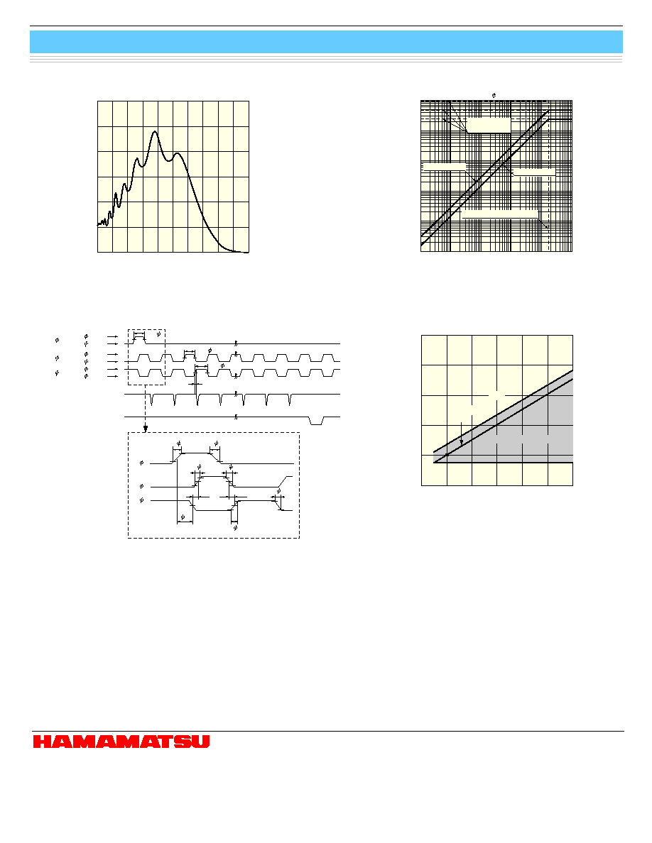
tvd
tpw 1
tpw 2
tpw s
st
V s (H)
V s (L)
V 1 (H)
V 1 (L)
V 2 (H)
V 2 (L)
1
2
END OF SCAN
st
1
2
tr s
tf s
tr 1
tf 1
X1
X2
t ov
tf 2
tr 2
ACTIVE VIDEO OUTPUT
10
≠5
10
2
10
1
10
0
10
≠1
10
≠2
10
≠3
10
≠4
10
≠3
10
≠2
10
≠1
10
0
OUTPUT CHARGE (pC)
EXPOSURE (
lx ∑
s)
(Typ. Vb=2 V, V =5 V, light source: 2856 K)
SATURATION
CHARGE
S3904-2048Q
S3901-1024Q
SATURATION EXPOSURE
0.3
0.2
0.1
0
200
400
600
800
1000
1200
WAVELENGTH (nm)
PHOTO SENSITIVITY (A/W)
(Ta=25 ∞C)
4
0
6
8
10
4
5
6
7
8
10
CLOCK PULSE AMPLITUDE (V)
VIDEO BIAS VOLTAGE (V)
2
9
MIN.
VIDEO BIAS RANGE
MAX.
RECOMMENDED BIAS
Figure 5 Spectral response (typical example)
Figure 6 Output charge vs. exposure
KMPDB0149EA
KMPDB0160EB
KMPDB0043EA
Figure 7 Timing chart
Figure 8 Video bias voltage margin
KMPDC0022EA
4