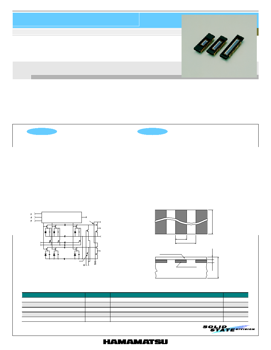
NMOS linear image sensors are self-scanning photodiode arrays designed specifically as detectors for multichannel spectroscopy. The scanning
circuit is made up of N-channel MOS transistors, operates at low power consumption and is easy to handle. Each photodiode has a large active
area, high UV sensitivity yet very low noise, delivering a high S/N even at low light levels. NMOS linear image sensors also offer excellent output
linearity and wide dynamic range.
S3921/S3924 series have a current-integration readout circuit utilizing the video line and an impedance conversion circuit. The output is available
in boxcar waveform allowing signal readout with a simple external circuit.
The photodiodes of S3921 series have a height of 2.5 mm and are arrayed in a row at a spacing of 50 µm. The photodiodes of S3924 series also
have a height of 2.5 mm but are arrayed at a spacing of 25 µm. The photodiodes are available in 3 different pixel quantities for each series, 128
(S3921-128Q), 256 (S3921-256Q, S3924-256Q) and 512 (S3921-512Q, S3924-512Q) and 1024 (S3924-1024Q). Quartz glass is the standard
window material.
Features
l Built-in current-integration readout circuit utilizing
video line capacitance and impedance conversion
circuit (boxcar waveform output)
l Wide active area
Pixel pitch: 50 µm (S3921 series)
25 µm (S3924 series)
Pixel height: 2.5 mm
l High UV sensitivity with good stability
l Low dark current and high saturation charge allow a long
integration time and a wide dynamic range at room temperature
l Excellent output linearity and sensitivity spatial uniformity
l Low voltage, single power supply operation
l Start pulse, clock pulse and video line reset pulse are
CMOS logic compatible
Applications
l Multichannel spectrophotometry
l Image readout system
I M A G E S E N S O R
NMOS linear image sensor
Voltage output type with current-integration readout circuit and impedance conversion circuit
S3921/S3924 series
b
a
2.5 mm
1.0 µm
1.0 µm
400 µm
OXIDATION SILICON
P TYPE SILICON
N TYPE SILICON
S3921 SERIES: a=50 µm, b=45 µm
S3924 SERIES: a=25 µm, b=20 µm
Figure 1 Equivalent circuit
Vss
START
st
CLOCK
CLOCK
1
2
ADDRESS
SWITCH
ADDRESS
SWITCH
ACTIVE
PHOTODIODE
DUMMY DIODE
RESET SWITCH
RESET
RESET V
ACTIVE VIDEO
Vdd
END OF SCAN
SOURCE FOLLOWER CIRCUIT
DIGITAL SHIFT RESISTER
(MOS SHIFT RESISTER)
SATURATION
CONTROL GATE
SATURATION
CONTROL DRAIN
DUMMY VIDEO
Figure 2 Active area structure
s
Absolute maximum ratings
Parameter
Symbol
Value
Unit
Supply voltage
Vdd
15
V
Input pulse (1, 2, st) voltage
V
15
V
Power consumption *
1
P
10
mW
Operating temperature *
2
Topr
-40 to +65
∞C
Storage temperature
Tstg
-40 to +85
∞C
*1: Vdd=5 V, Vr=2.5 V
*2: No condensation
KMPDC0019EA
KMPDA0067EA
NMOS linear image sensor
S3921/S3924 series
s
Shape specifications
Parameter
S3921-
128Q
S3921-
256Q
S3921-
512Q
S3924-
256Q
S3924-
512Q
S3924-
1024Q
Unit
Number of pixels
128
256
512
256
512
1024
-
Package length
31.75
40.6
31.75
40.6
mm
Number of pin
22
22
-
Window material *
3
Quartz
Quartz
-
Weight
3.0
3.5
3.0
3.5
g
*3: Fiber optic plate is available.
s
Specifications (Ta=25 ∞C)
S3921 series
S3924 series
Parameter
Symbol
Min.
Typ.
Max.
Min.
Typ.
Max.
Unit
Pixel pitc h
-
-
50
-
-
25
-
µm
Pixel height
-
-
2.5
-
-
2.5
-
mm
Spectral response range (10 % of peak)
200 to 1000
200 to 1000
nm
Peak sensitivity wavelength
p
-
600
-
-
600
-
nm
Photodiode dark current *
4
I
D
-
0.2
0.6
-
0.1
0.3
pA
Photodiode capacitance *
4
Cph
-
20
-
-
10
-
pF
Saturation exposure *
4,
*
5
Esat
-
220
-
-
220
-
mlx ∑ s
Saturation charge *
4
Qsat
-
50
-
-
25
-
pC
-
1350 (-128Q)
-
-
1050 (-256Q)
-
mV
-
1300 (-256Q)
-
-
820 (-512Q)
-
mV
Saturation output voltage *
4
Vsat
-
1100 (-512Q)
-
-
570 (-1024Q)
-
mV
Photo response non-uniformity *
6
PRNU
-
-
±3
-
-
±3
%
*4: Reset V=2.5 V, Vdd=5.0 V, V=5.0 V
*5: 2856 K, tungsten lamp
*6: 50 % of saturation, excluding the start pixel and last pixel
s
Electrical characteristics (Ta=25 ∞C)
S3921 series
S3924 series
Parameter
Symbol
Condition
Min.
Typ.
Max.
Min.
Typ.
Max.
Unit
High V1, V2 (H)
-
4.5
5
10
4.5
5
10
V
Clock pulse (1, 2)
voltage
Low V1, V2 (L)
-
0
-
0.4
0
-
0.4
V
High
Vs (H)
-
4.5
V
10
4.5
V
10
V
Start pulse (st) voltage *
7
Low
Vs (L)
-
0
-
0.4
0
-
0.4
V
High
Vr (H)
-
4.5
V
10
4.5
V
10
V
Reset pulse (Reset )
voltage *
7
Low
Vr (L)
-
0
-
0.4
0
-
0.4
V
Source follower circuit drain voltage *
%
Vdd
-
4.5
V
10
4.5
V
10
V
Reset voltage (Reset V) *
8
Vr
-
2.0
V - 2.5 V - 2.0
2.0
V - 2.5 V - 2.0
V
Saturation control gate voltage
Vscg
-
-
0
-
-
0
-
V
Saturation control drain voltage *
8
Vscd
-
-
Vr
-
-
Vr
-
V
Clock pulse (1, 2) rise / fall time
tr1, tr2
tf1, tf2
-
-
20
-
-
20
-
ns
Clock pulse (1, 2) pulse width
tpw1, tpw2
-
200
-
-
200
-
-
ns
Start pulse (st) rise / fall time
trs, tfs
-
-
20
-
-
20
-
ns
Start pulse (st) pulse width
tpws
-
200
-
-
200
-
-
ns
Reset pulse rise / fall time
trr, tfr
-
-
20
-
-
20
-
ns
Start pulse (st) and clock pulse
(2) overlap
tov
-
200
-
-
200
-
-
ns
Clock pulse (2) and reset
pulse (Reset ) overlap
tovr
-
660
-
-
660
-
-
ns
Clock pulse (2) and reset
pulse (Reset ) delay time
tdr-2
-
50
-
-
50
-
-
ns
Clock pulse (1, 2) space *
9
X
1
, X
2
-
trf - 20
-
-
trf - 20
-
-
ns
Clock pulse (2, Reset ) space *
9
tsr-2
-
0
-
-
0
-
-
ns
Data rate *
10
f
-
0.1
-
500
0.1
-
500
kHz
-
100 (-128 Q)
-
-
100 (-256 Q)
-
ns
-
150 (-256 Q)
-
-
150 (-512 Q)
-
ns
Video delay time
tvd
50 % of
saturation
*
-
200 (-512 Q)
-
-
200 (-1024 Q)
-
ns
-
21 (-128 Q)
-
-
27 (-256 Q)
-
pF
-
36 (-256 Q)
-
-
50 (-512 Q)
-
pF
Clock pulse (1, 2)
line capacitance
C
5 V bias
-
67 (-512 Q)
-
-
100 (-1024 Q)
-
pF
Reset pulse (Reset )
line capacitance
Cr
5 V bias
-
6
-
-
6
-
pF
-
12 (-128 Q)
-
-
14 (-256 Q)
-
pF
-
20 (-256 Q)
-
-
24 (-512 Q)
-
pF
Saturation control gate (Vscg)
line capacitance
Cscg
5 V bias
-
35 (-512 Q)
-
-
45 (-1024 Q)
-
pF
Output impedance
Zo
Vdd=5 V
Vr=2.5 V
-
200
-
-
200
-
*7: V is input pulse voltage (refer to figure 8)
*8: Terminal pin 7 is used for both Reset V and saturation control drain voltage
*9: trf is the clock pulse rise or fall time. A clock pulse space of
rise time/fall time - 20
ns (nanoseconds) or more
should be input if the clock pulse rise or fall time is longer than 20
ns. (refer to figure 7)
*10: Reset V=2.5 V, Vdd=5.0 V, V=5.0 V

NMOS linear image sensor
S3921/S3924 series
Figure 3 Dimensional outlines (unit: mm)
S3921-128Q, S3924-256Q
S3921-256Q, S3924-512Q
0.51
25.4
2.54
3.0
31.75
10.4
5.4 ± 0.2
5.0 ± 0.2
3.2 ± 0.3
ACTIVE AREA
6.4 ◊ 2.5
0.25
10.16
1.3 ± 0.2*
PHOTOSENSITIVE
SURFACE
* Optical distance from the outer surface
of the quartz window to the chip surface
0.51
25.4
2.54
3.0
ACTIVE AREA
12.8 ◊ 2.5
6.4 ± 0.3
31.75
10.4
5.4 ± 0.2
5.0 ± 0.2
0.25
10.16
1.3 ± 0.2*
PHOTOSENSITIVE
SURFACE
* Optical distance from the outer surface
of the quartz window to the chip surface
S3921-512Q, S3924-1024Q
0.51
25.4
3.0
40.6
10.4
5.4 ± 0.2
5.0 ± 0.2
12.8 ± 0.3
ACTIVE AREA
25.6 ◊ 2.5
0.25
10.16
1.3 ± 0.2 *
PHOTOSENSITIVE
SURFACE
* Optical distance from the outer surface
of the quartz window to the chip surface
2.54
2
1
st
Vss
Vscg
RESET
RESET V (Vscd)
Vss
ACTIVE VIDEO
DUMMY VIDEO
Vsub
NC
NC
NC
NC
NC
NC
NC
NC
NC
END OF SCAN
Vdd
1
2
3
4
5
6
7
8
9
10
11
22
21
20
19
18
17
16
15
14
13
12
Vss, Vsub and NC should be grounded.
Figure 4 Pin connection
KMPDC0025EA
KMPDA0060EA
KMPDA0061EA
KMPDA0062EA

NMOS linear image sensor
S3921/S3924 series
Terminal
Input or output
Description
1, 2
Input
(CMOS logic compatible)
Pulses for operating the MOS shift register. The video data rate is equal
to the clock pulse frequency since the video output signal is obtained
synchronously with the rise of 2 pulse.
st
Input
(CMOS logic compatible)
Pulse for starting the MOS shift register operation. The time interval
between start pulses is equal to the signal accumulation time.
Vss
-
Connected to the anode of each photodiode. This should be grounded.
Vscg
Input
Used for restricting blooming. This should be grounded.
Reset
Input
(CMOS logic compatible)
With Reset at high level, the video line is reset at the Reset V voltage.
Reset V
Input
The Reset V terminal connects to each photodiode cathode via the video
line when the address turns on. A positive voltage should be applied to
the Reset V terminal to use each photodiode at a reverse bias. Setting
the Reset V voltage to 2.5 V is recommended when the amplitude of 1,
2 and Reset is 5 V. Terminal pin 7 is used for both Reset V and Vscd.
Vscd
Input
Used for restricting blooming. This should be biased at a voltage equal
to Reset V.
Active video
Output
Low-impedance video output signal after internal current-voltage
conversion. Negative-going output including DC offset.
Dummy video
Output
This has the same structure as the active video, but is not connected to
photodiodes, so only DC offset is output. Leave this terminal open when
not used.
Vsub
-
Connected to the silicon substrate. This should be grounded.
Vdd
Input
Supply voltage to the internal impedance conversion circuit. A voltage
equal to the amplitude of each clock should be applied to this terminal.
End of scan
Output
(CMOS logic compatible)
This should be pulled up at 5 V by using a 10 k resistor. This is a
negative going pulse that appears synchronously with the 2 timing
right after the last photodiode is addressed.
NC
-
Should be grounded.
s Construction of image sensor
The NMOS image sensor consists of a scanning circuit made
up of MOS transistors, a photodiode array, and a switching
transistor array that addresses each photodiode, all integrated
onto a monolithic silicon chip. Figure 1 shows the circuit of a
NMOS linear image sensor.
The MOS scanning circuit operates at low power consump-
tion and generates a scanning pulse train by using a start
pulse and 2-phase clock pulses in order to turn on each ad-
dress sequentially. Each address switch is comprised of an
NMOS transistor using the photodiode as the source, the
video line as the drain and the scanning pulse input section
as the gate.
The photodiode array operates in charge integration mode
so that the output is proportional to the amount of light expo-
sure (light intensity ◊ integration time).
Each cell consists of an active photodiode and a dummy
diode, which are respectively connected to the active video
line and the dummy video line via a switching transistor. Each
of the active photodiodes is also connected to the saturation
control drain via the saturation control gate, so that the photo-
diode blooming can be suppressed by grounding the satura-
tion control gate. Applying a pulse signal to the saturation
control gate triggers all reset. (See "Auxiliary functions".)
10
-5
10
1
10
0
10
-1
10
-2
10
-3
10
-4
10
-4
10
-3
10
-2
10
-1
10
0
OUTPUT VOLTAGE (V)
EXPOSURE (lx ∑ s)
(Typ. Reset V=2.5 V, Vdd=5.0 V, V =5 V, light source: 2856 K)
SATURATION EXPOSURE
S3921-512Q
S3921-128Q
S3921-256Q
SATURATION VOLTAGE
0.3
0.2
0.1
0
200
400
600
800
1000
1200
WAVELENGTH (nm)
PHOTO SENSITIVITY (A/W)
(Ta=25 ∞C)
10
-5
10
1
10
0
10
-1
10
-2
10
-3
10
-4
10
-4
10
-3
10
-2
10
-1
10
0
OUTPUT VOLTAGE (V)
EXPOSURE (lx ∑ s)
S3924-1024Q
S3924-256Q
SATURATION VOLTAGE
(Typ. Reset V=2.5 V, Vdd=5.0 V, V =5 V, light source: 2856 K)
S3924-512Q
SATURATION EXPOSURE
KMPDB0149EA
KMPDB0118EA
KMPDB0119EA
Figure 5 Spectral response (typical example) Figure 6 Output voltage vs. exposure
NMOS linear image sensor
S3921/S3924 series
Figure 2 shows the schematic diagram of the photodiode
active area. This active area has a PN junction consisting of
an N-type diffusion layer formed on a P-type silicon substrate.
A signal charge generated by light input accumulates as a
capacitive charge in this PN junction. The N-type diffusion
layer provides high UV sensitivity but low dark current.
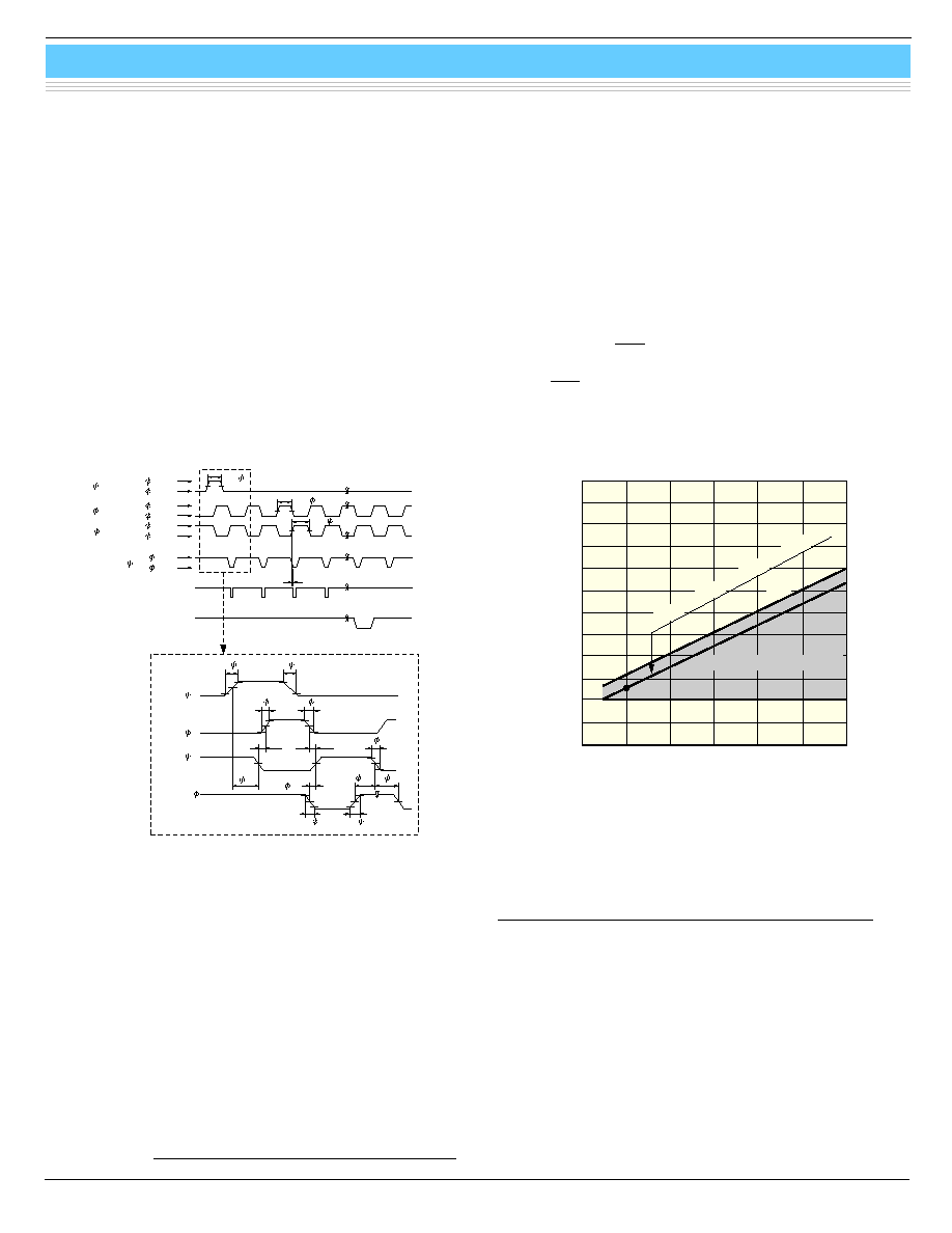
s Driver circuit
A start pulse
st and 2-phase clock pulses 1, 2 are needed
to drive the shift register. These start and clock pulses are
positive going pulses and CMOS logic compatible.
The 2-phase clock pulses
1, 2 can be either completely
separated or complementary. However, both pulses must not
be "High" at the same time.
A clock pulse space (X
1
and X
2
in Figure 7) of a "rise time/fall
time - 20" ns or more should be input if the rise and fall times
of
1, 2 are longer than 20 ns. The 1 and 2 clock pulses
must be held at "High" at least 200 ns. Since the photodiode
signal is obtained at the rise of each
2 pulse, the clock pulse
frequency will equal the video data rate.
The amplitude of start pulse
st is the same as the 1 and 2
pulses. The shift register starts the scanning at the "High"
level of
st, so the start pulse interval is equal to signal accu-
mulation time. The
st pulse must be held "High" at least 200
ns and overlap with
2 at least for 200 ns. To operate the shift
register correctly,
2 must change from the "High" level to the
"Low" level only once during "High" level of
st. The timing
chart for each pulse is shown in Figure 7.
s End of scan
The end of scan (EOS) signal appears in synchronization
with the
2 timing right after the last photodiode is addressed,
and the EOS terminal should be pulled up at 5 V using a 10
k
resistor.
tvd
tpw 1
tpw 2
tf s
tr 1
tf 1
X1
X2
t ov
ts r-2
tf 2
RESET
Vr (H)
Vr (L)
td r-2
t ovr
tfr
trr
st
V s (H)
V s (L)
V 1 (H)
V 1 (L)
V 2 (H)
V 2 (L)
1
2
END OF SCAN
ACTIVE VIDEO OUTPUT
tpw s
tr s
st
1
2
RESET
Figure 7 Timing chart for driver circuit
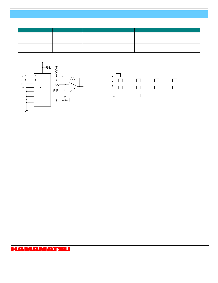
s Signal readout circuit
S3921/S3924 series include a current integration circuit uti-
lizing the video line capacitance and an impedance conver-
sion circuit. This allows signal readout with a simple external
circuit. However, a positive bias must be applied to the video
line because the photodiode anode of NMOS linear image
sensors is at 0 V (Vss). This is done by adding an appropriate
pulse to the reset
terminal. The amplitude of the reset pulse
should be equal to
1, 2 and st.
When the reset pulse is at the high level, the video line is set
at the Reset V voltage. Figure 8 shows the Reset V voltage
margin. A higher clock pulse amplitude allows higher Reset
V voltage and saturation charge. Conversely, if the Reset V
voltage is set at a low level with a higher clock pulse ampli-
tude, the rise and fall times of video output waveform can be
shortened. Setting the Reset V voltage to 2.5 V is recom-
mended when the amplitude of
1, 2, st and Reset is 5 V.
To obtain a stable output, an overlap between the reset pulse
(Reset
) and 2 must be settled. (Reset must rise while 2
is at the high level.) Furthermore, Reset
must fall while 2 is
at the low level.
S3921/S3924 series provide output signals with negative-
going boxcar waveform which include a DC offset of approxi-
mately 1 V when Reset V is 2.5 V. If you want to remove the DC
offset to obtain the positive-going output, the signal readout
circuit and pulse timing shown in Figure 9 are recommended.
In this circuit, Rs must be larger than 10 k
. Also, the gain is
determined by the ratio of Rf to Rs, so choose the Rf value
that suits your application.
Figure 8 Reset V voltage margin
4
0
6
8
10
12
4
5
6
7
8
10
CLOCK PULSE AMPLITUDE (V)
RESET V VOLTAGE (V)
2
9
MIN.
RESET
V VOLTAGE RANGE
MAX.
RECOMMENDED RESET
V VOLTAGE
KMPDC0026EA
KMPDB0047EA
HAMAMATSU PHOTONICS K.K., Solid State Division
1126-1 Ichino-cho, Hamamatsu City, 435-8558 Japan, Telephone: (81) 053-434-3311, Fax: (81) 053-434-5184, http://www.hamamatsu.com
U.S.A.: Hamamatsu Corporation: 360 Foothill Road, P.O.Box 6910, Bridgewater, N.J. 08807-0910, U.S.A., Telephone: (1) 908-231-0960, Fax: (1) 908-231-1218
Germany: Hamamatsu Photonics Deutschland GmbH: Arzbergerstr. 10, D-82211 Herrsching am Ammersee, Germany, Telephone: (49) 08152-3750, Fax: (49) 08152-2658
France: Hamamatsu Photonics France S.A.R.L.: 8, Rue du Saule Trapu, Parc du Moulin de Massy, 91882 Massy Cedex, France, Telephone: 33-(1) 69 53 71 00, Fax: 33-(1) 69 53 71 10
United Kingdom: Hamamatsu Photonics UK Limited: 2 Howard Court, 10 Tewin Road, Welwyn Garden City, Hertfordshire AL7 1BW, United Kingdom, Telephone: (44) 1707-294888, Fax: (44) 1707-325777
North Europe: Hamamatsu Photonics Norden AB: Smidesv‰gen 12, SE-171 41 Solna, Sweden, Telephone: (46) 8-509-031-00, Fax: (46) 8-509-031-01
Italy: Hamamatsu Photonics Italia S.R.L.: Strada della Moia, 1/E, 20020 Arese, (Milano), Italy, Telephone: (39) 02-935-81-733, Fax: (39) 02-935-81-741
Information furnished by HAMAMATSU is believed to be reliable. However, no responsibility is assumed for possible inaccuracies or omissions.
Specifications are subject to change without notice. No patent rights are granted to any of the circuits described herein. ©2001 Hamamatsu Photonics K.K.
NMOS linear image sensor
S3921/S3924 series
Cat. No. KMPD1044E01
Apr. 2001 DN
Vscg
Vss
Vsub
NC
EOS
EOS
10 k
+5 V
+5 V
+
≠
OPEN
DUMMY
VIDEO
ACTIVE
VIDEO
Reset
+2.5 V
Reset V
(Vscd)
+
+
+15 V
Rs 10 k
Rf
Vdd
st
2
1
st
2
1
Reset
Reset
st
2
1
s Anti-blooming function
If the incident light intensity is higher than the saturation charge level, even partially, a signal charge in excess of the saturation
charge cannot accumulate in the photodiode. This excessive charge flows out into the video line degrading the signal purity. To
avoid this problem and maintain the signal purity, applying the same voltage as the Reset V voltage to the saturation control drain
and grounding the saturation control gate are effective. If the incident light intensity is extremely high, a positive bias should be
applied to the saturation control gate. The larger the voltage applied to the saturation control gate, the higher the function for
suppressing the excessive saturation charge will be. However, this voltage also lowers the amount of saturation charge, so an
optimum bias voltage should be selected.
s Auxiliary functions
1) All reset
In normal operation, the accumulated charge in each photodiode is reset when the signal is read out. Besides this method that
uses the readout line, S3921/S3924 series can reset the photodiode charge by applying a pulse to the saturation control gate.
The amplitude of this pulse should be equal to the
1, 2, st, Reset pulses and the pulse width should be longer than 5 µs.
When the saturation control gate is set at the "High" level, all photodiodes are reset to the saturation control drain potential.
Conversely, when the saturation control gate is set at the "Low" level (0 V), the signal charge accumulates in each photodiode
without being reset.
2) Dummy video
S3921/S3924 series have a dummy video line. Positive-polarity video signals with the DC offset remove can be obtained by
differential amplification of the active video line and dummy video line outputs. When not needed, leave this unconnected.
s Precautions for using NMOS linear image sensors
1) Electrostatic countermeasures
NMOS linear image sensors are designed to resist static electrical charges. However, take sufficient cautions and countermea-
sures to prevent damage from static charges when handling the sensors.
2) Window
If dust or grime sticks to the surface of the light input window, it appears as a black blemish or smear on the image. Before using
the image sensor, the window surface should be cleaned. Wipe off the window surface with a soft cloth, cleaning paper or
cotton swab slightly moistened with organic solvent such as alcohol, and then lightly blow away with compressed air. Do not
rub the window with dry cloth or cotton swab as this may generate static electricity.
KMPDC0027EA
KMPDC0028EA
Product name
Type No.
Content
Feature
C7885
Low cost driver circuit
Driver circuit
C7885G
C7885 + C8225-02
Low price
Single power supply (+15 V) operation
Boxcar waveform output
Pulse generator
C8225-02
C7885 series
Cable
A8226
C7883 to C7885 series
BNC, length 1 m
Figure 9 Readout circuit example and timing chart
Hamamatsu provides the following driver circuits and related products (sold separately).