
S4111-16Q and S4111-16R are 16-element Si photodiode arrays in a ceramic DIP package. These photodiode arrays are chiefly developed for
low-light-level detection such as spectrophotometers. S4111-16Q uses a quartz window that covers a wide spectral response range from UV
through near infrared light. S4111-16R uses a resin coating window that provides a spectral response range from the visible to near infrared light.
Since all elements can be used with a reverse voltage for charge storage readout, S4111-16Q and S4111-16R are able to detect low level light
with high sensitivity. Cross-talk between elements is minimized to maintain signal purity.
P H O T O D I O D E
PRELIMINARY DATA
Jan. 2002
S4111-16Q/-16R
Si photodiode array
16-element photodiode array
Features
l
Active area: 0.9 ◊ 1.45 mm (◊ 16 elements)
l
S4111-16Q: for UV through near infrared detection
S4111-16R: for visible to near infrared detection
l
Low cross-talk
Applications
l
Low-light-level detection
l
Spectrophotometers
l
Position detection
s
s
s
s Absolute maximum ratings (Ta=25
∞
C)
Parameter
Symbol
Value
Unit
Reverse voltage
V
R
Max.15
V
Operating
temperature
Topr
-20 to +60
∞
C
Storage
temperature
Tstg
-20 to +80
∞
C
s Electrical and optical characteristics (Ta=25
∞
C, per 1 element)
S4111-16Q
S4111-16R
Parameter
Symbol
Condition
Min.
Typ.
Max.
Min.
Typ.
Max.
Unit
Spectral
response range
-
190 to
1100
-
-
320 to
1100
-
nm
Peak sensitivity
wavelength
p
-
960
-
-
960
-
nm
=633 nm
-
0.43
-
-
0.40
-
A/W
Photo sensitivity
S
=
p
-
0.58
-
-
0.58
-
A/W
I
D
1
V
R
=10 mV
-
1
5
-
1
5
pA
Dark current
I
D
2
V
R
=10 V
-
5
25
-
5
25
pA
Shunt resistance
Rsh
V
R
=10 mV
2
10
-
2
10
-
G
Ct1
V
R
=0 V, f=10 kHz
-
200
-
-
200
-
pF
Terminal
capacitance
Ct2
V
R
=10 V, f=10 kHz
-
50
-
-
50
-
pF
Rise time
tr
V
R
=0 V, R
L
=1 k
10 to 90 %
-
0. 5
-
-
0. 5
-
µs
Noise equivalent
power
NEP
=
p
-
2.0 ◊ 10
-16
-
-
2.0 ◊ 10
-16
-
W/Hz
1/2
1
Si photodiode array
S4111-16Q/-16R
HAMAMATSU PHOTONICS K.K., Solid State Division
1126-1 Ichino-cho, Hamamatsu City, 435-8558 Japan, Telephone: (81) 053-434-3311, Fax: (81) 053-434-5184, http://www.hamamatsu.com
U.S.A.: Hamamatsu Corporation: 360 Foothill Road, P.O.Box 6910, Bridgewater, N.J. 08807-0910, U.S.A., Telephone: (1) 908-231-0960, Fax: (1) 908-231-1218
Germany: Hamamatsu Photonics Deutschland GmbH: Arzbergerstr. 10, D-82211 Herrsching am Ammersee, Germany, Telephone: (49) 08152-3750, Fax: (49) 08152-2658
France: Hamamatsu Photonics France S.A.R.L.: 8, Rue du Saule Trapu, Parc du Moulin de Massy, 91882 Massy Cedex, France, Telephone: 33-(1) 69 53 71 00, Fax: 33-(1) 69 53 71 10
United Kingdom: Hamamatsu Photonics UK Limited: 2 Howard Court, 10 Tewin Road, Welwyn Garden City, Hertfordshire AL7 1BW, United Kingdom, Telephone: (44) 1707-294888, Fax: (44) 1707-325777
North Europe: Hamamatsu Photonics Norden AB: Smidesv‰gen 12, SE-171 41 Solna, Sweden, Telephone: (46) 8-509-031-00, Fax: (46) 8-509-031-01
Italy: Hamamatsu Photonics Italia S.R.L.: Strada della Moia, 1/E, 20020 Arese, (Milano), Italy, Telephone: (39) 02-935-81-733, Fax: (39) 02-935-81-741
Information furnished by HAMAMATSU is believed to be reliable. However, no responsibility is assumed for possible inaccuracies or omissions.
Specifications are subject to change without notice. No patent rights are granted to any of the circuits described herein. ©2002 Hamamatsu Photonics K.K.
Cat. No. KMPD1061E01
Jan. 2002 DN
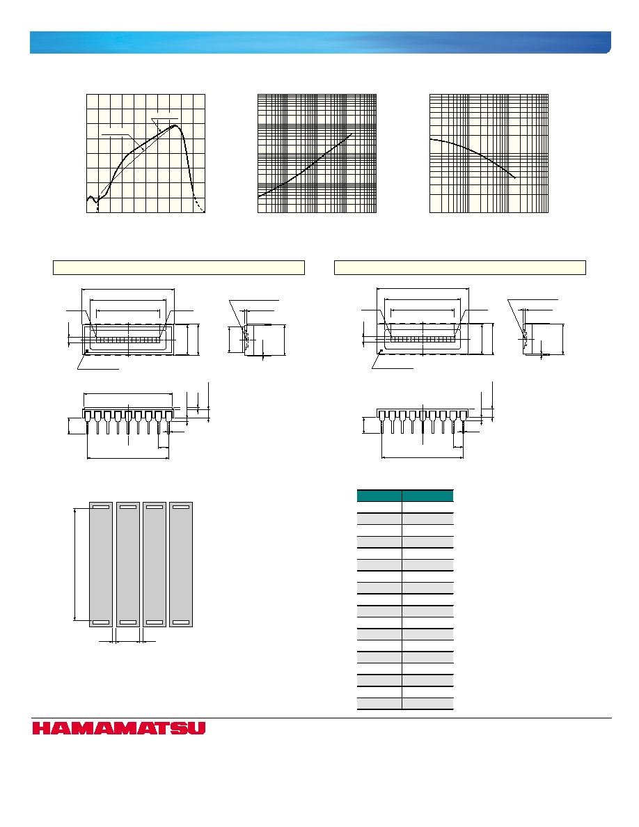
s
Dimensional outlines (unit: mm)
s
Spectral response
0.8
0.7
0.6
0.5
0.4
0.3
0.2
0.1
0
190
400
600
800
1000
1200
WAVELENGTH (nm)
PHOTO SENSITIVITY (A/W)
(Typ. Ta=25 ∞C)
S4111-16Q
S4111-16R
s
Dark current vs. reverse voltage
s
Terminal capacitance vs.
reverse voltage
0.01
0.1
1
10
100
100 fA
10 fA
1 pA
10 pA
100 pA
REVERSE VOLTAGE (V)
DARK CURRENT
(Typ. Ta=25 ∞C)
0.1
1
10
100
10 pF
100 pF
1 nF
REVERSE VOLTAGE (V)
TERMINAL CAPACITANCE
(Typ. Ta=25 ∞C)
P 2.54 ◊ 8 = 20.32
22.86 ± 0.3
18.8
(22.0)
2.2 ± 0.3
(0.5)
2.54
(4.5)
INDEX MARK
7.87 ± 0.3
7.49 ± 0.2
1
2
3
4
5
6
7
0.46
7.62 ± 0.3
0.5 ± 0.2
6.5
PHOTOSENSITIVE
SURFACE
9
8
18
17 16 15 14 13 12
10
11
0.25
ACTIVE AREA
15.9
QUARTZ GLASS
CH 1
CH 16
1.45
0.9 ± 0.3
P 2.54 ◊ 8 = 20.32
22.86 ± 0.3
18.8
ACTIVE AREA
15.9
2.2 ± 0.3
2.54
(4.5)
INDEX MARK
1.45
7.87 ± 0.3
7.49 ± 0.2
1
2
3
4
5
6
7
8
9
18
17 16 15 14 13 12 11
10
0.46
7.62 ± 0.3
0.5 ± 0.2
PHOTOSENSITIVE
SURFACE
0.25
CH 1
CH 16
0.9
± 0.3
s
Details of elements (unit: mm)
1.45
0.9
0.1
0.1
KMPDB0190EA
KMPDB0191EA
KMPDB0192EA
KMPDA0135EA
KMPDA0136EA
KMPDA0145EA
S4111-16Q
S4111-16R
s Pin connection
Pin No.
Element No.
1
Cathode
2
2
3
4
4
6
5
8
6
10
7
12
8
14
9
16
10
Cathode
11
15
12
13
13
11
14
9
15
7
16
5
17
3
18
1
2