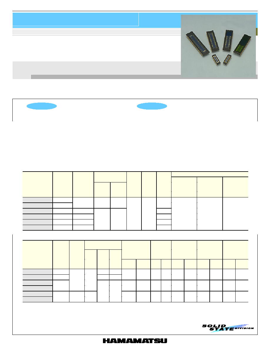
S4111/S4114 series
S4111/S4114 series are Si photodiode linear array mounted in ceramic DIPs (Dual Inline Packages). These photodiode arrays are primarily
developed for low-light-level detection such as spectrophotometry, and cover a wide spectral range from UV to near infrared light. Since all
elements can be used with a reverse bias for charge storage readout, S4111/S4114 series are able to detect low level light with high sensitivity.
Cross-talk between elements is minimized to maintain signal purity. Special filters can be attached as the input window.
P H O T O D I O D E
Si photodiode array
16, 35, 46 element Si photodiode array for UV to NIR
Features
l Large active area
l Low cross-talk
l Wide spectral response range
l High UV sensitivity
l Wide linearity
l S4111 series: Enhanced infrared sensitivity,
low dark current
l S4114 series: Low terminal capacitance,
high-speed response
Applications
l Multichannel spectrophotometers
l Color analyzers
l Light spectrum analyzers
l Light position detection
s
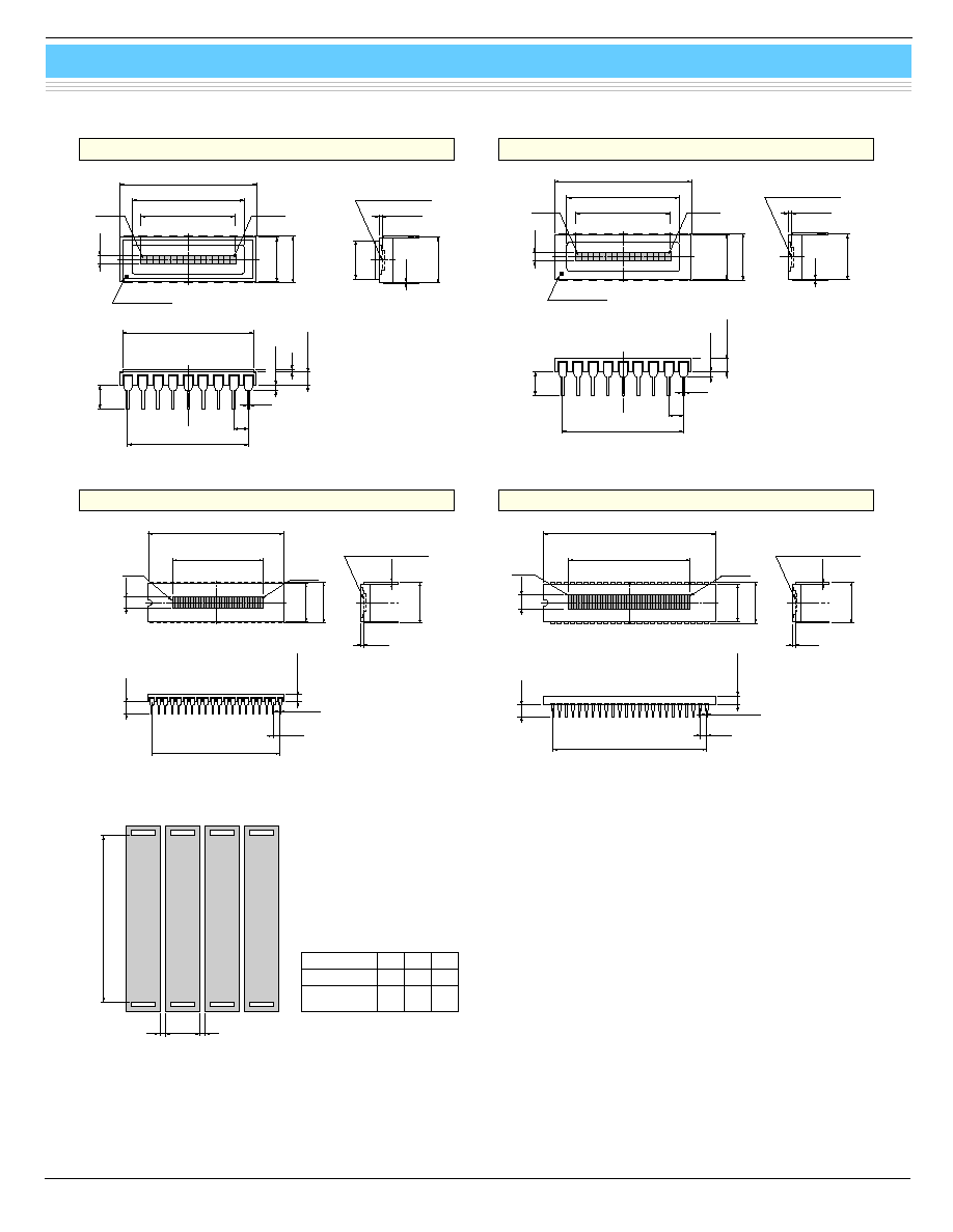
General ratings / Absolute maximum ratings
Absolute maximum ratings
Active area
(per 1 element)
Package
Size Effective
area
Between
elements
measure
Between
elements
pitch
Reverse
voltage
V
R
Max.
Operating
temperature
Topr
Storage
temperature
Tstg
Type No.
Dimensional
outline/
Window
material *
(mm)
(mm)
(mm
2
)
(mm)
(mm)
Number
of
elements
(V)
(�C)
(�C)
S4111-16Q
/Q
S4111-16R
/R
18 pin DIP 1.45 � 0.9 1.305
16
S4111-35Q
/Q
40 pin DIP
35
S4111-46Q
/Q
48 pin DIP
46
S4114-35Q
/Q
40 pin DIP
35
S4114-46Q
/Q
48 pin DIP
4.4 � 0.9 3.96
0.1
1.0
46
15
-20 to +60
-20 to +80
s
Electrical and optical characteristics (Typ. Ta=25 �C, per 1 element, unless otherwise noted)
Photo sensitivity
S
Spectral
response
range
Peak
sensitivity
wavelength
p
p 200 nm 633 nm
Dark current
I
D
Max.
Shunt
resistance
Rsh
V
R
=10 mV
Terminal
capacitance
Ct
Rise time
tr
R
L
=1 k
=655 nm
NEP
=p
Type No.
(nm)
(nm) (A/W) (A/W) (A/W)
V
4
=10 mV
(pA)
V
4
=10 V
(pA)
Min
(G)
Typ.
(G)
V
4
=0 V
(pF)
V
4
=10 V
(pF)
V
R
=0 V
(�s)
V
4
=10 V
(�s)
V
4
=10 mV
(W/Hz
1/2
)
V
4
=10 V
(W/Hz
1/2
)
S4111-16Q
190 to 1100
0.08 0.43
S4111-16R
320 to 1100
-
0.39
5
25
2.0 250 200
50
0.5
0.1 2.0 � 10
-16
1.7 � 10
-15
S4111-35Q
S4111-46Q
190 to 1100
960
0.58
10
50
1.0
30
550
120
1.2
0.3 5.6 � 10
-16
3.1 � 10
-15
S4114-35Q
S4114-46Q
190 to 1000 800
0.50
0.08 0.43
60
300
0.15
2
35
20
0.1
0.05 2.5 � 10
-15
8.0 � 10
-15
* Window material R: resin coating, Q: quartz glass
Si photodiode array
S4111/S4114 series
HAMAMATSU PHOTONICS K.K., Solid State Division
1126-1 Ichino-cho, Hamamatsu City, 435-8558 Japan, Telephone: (81) 053-434-3311, Fax: (81) 053-434-5184, http://www.hamamatsu.com
U.S.A.: Hamamatsu Corporation: 360 Foothill Road, P.O.Box 6910, Bridgewater, N.J. 08807-0910, U.S.A., Telephone: (1) 908-231-0960, Fax: (1) 908-231-1218
Germany: Hamamatsu Photonics Deutschland GmbH: Arzbergerstr. 10, D-82211 Herrsching am Ammersee, Germany, Telephone: (49) 08152-3750, Fax: (49) 08152-2658
France: Hamamatsu Photonics France S.A.R.L.: 8, Rue du Saule Trapu, Parc du Moulin de Massy, 91882 Massy Cedex, France, Telephone: 33-(1) 69 53 71 00, Fax: 33-(1) 69 53 71 10
United Kingdom: Hamamatsu Photonics UK Limited: 2 Howard Court, 10 Tewin Road, Welwyn Garden City, Hertfordshire AL7 1BW, United Kingdom, Telephone: (44) 1707-294888, Fax: (44) 1707-325777
North Europe: Hamamatsu Photonics Norden AB: Smidesv�gen 12, SE-171 41 Solna, Sweden, Telephone: (46) 8-509-031-00, Fax: (46) 8-509-031-01
Italy: Hamamatsu Photonics Italia S.R.L.: Strada della Moia, 1/E, 20020 Arese, (Milano), Italy, Telephone: (39) 02-935-81-733, Fax: (39) 02-935-81-741
Information furnished by HAMAMATSU is believed to be reliable. However, no responsibility is assumed for possible inaccuracies or omissions.
Specifications are subject to change without notice. No patent rights are granted to any of the circuits described herein. �2001 Hamamatsu Photonics K.K.
Cat. No. KMPD1002E04
Mar. 2001 DN
s
Pin connections
Pin No.
16-element
type
35-element
type
46-element
type
1
KC
KC
KC
2
2
2
2
3
4
4
4
4
6
6
6
5
8
8
8
6
10
10
10
7
12
12
12
8
14
14
14
9
16
16
16
10
KC
18
18
11
15
NC
20
12
13
20
22
13
11
22
24
14
9
24
26
15
7
26
28
16
5
28
30
17
3
30
32
18
1
32
34
19
34
36
20
*
1
38
21
KC
40
22
35
42
23
33
44
24
31
46
25
29
KC
26
27
45
27
25
43
28
23
41
29
21
39
30
19
37
31
17
35
32
15
33
33
13
31
34
11
29
35
9
27
36
7
25
37
5
23
38
3
21
39
1
19
40
*
1
17
41
15
42
13
43
11
44
9
45
7
46
5
47
3
48
1
*1: Please open it.
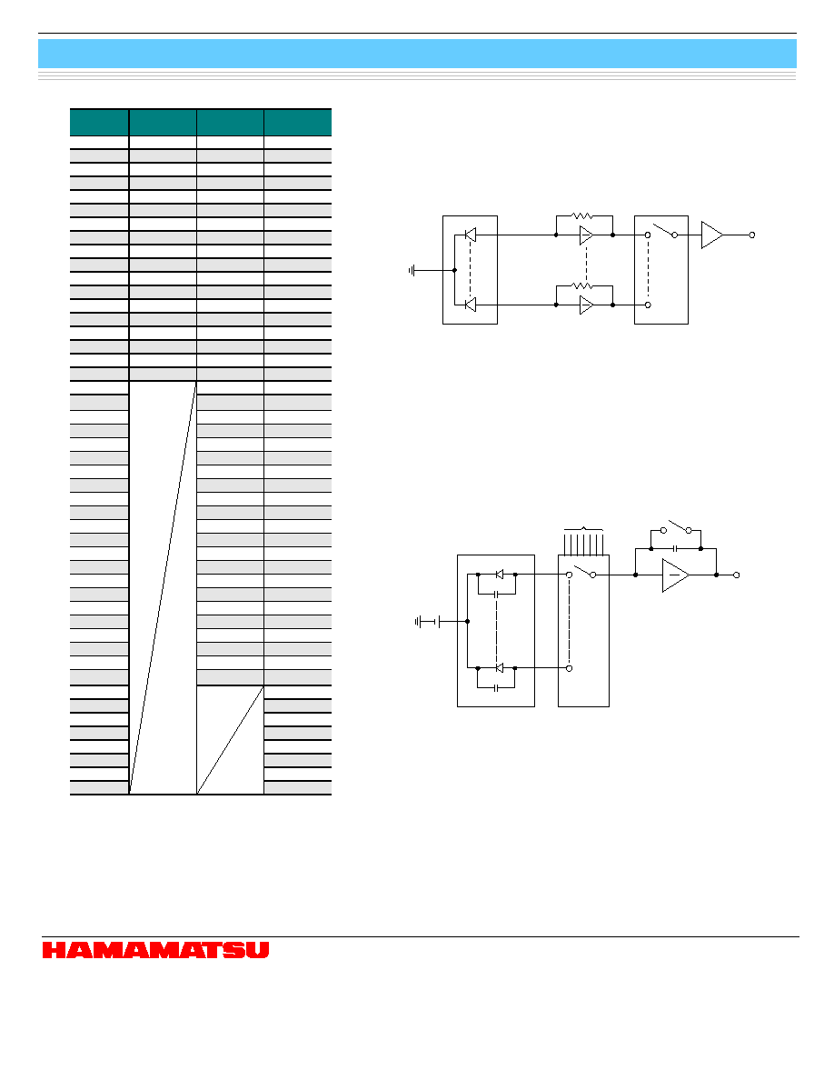
s Operating circuits
In the most generally used circuit, operational amplifiers are con-
nected to each channel to read the output in real time. The output of
an operational amplifier is of low impedance and thus can be easily
multiplexed.
In the charge storage readout method, the charge stored in the
junction capacitance of each channel, which is proportional to the
incident light intensity, can be read out in sequence by a multiplexer.
With this method, reverse voltage must be applied to the
photodiodes, so S4111 and S4114 series are suitable. One amplifier
is sufficient but care should be taken regarding noise, dynamic
range, etc.
PHOTODIODE ARRAY
ADDRESS
MULTIPLEXER
BIAS
KMPDC0002EA
PHOTODIODE ARRAY
MULTIPLEXER
KMPDC0001EA