 | –≠–ª–µ–∫—Ç—Ä–æ–Ω–Ω—ã–π –∫–æ–º–ø–æ–Ω–µ–Ω—Ç: S4282-51 | –°–∫–∞—á–∞—Ç—å:  PDF PDF  ZIP ZIP |
Features
l
Large allowable background light level
S4282-51, S6986 : 10000
lx
Typ.
S6809, S6846, S7136/-10: 3000
lx
Typ.
l
Minimum detection level
S4282-51, S6986 : 0.7 µW/mm
2
Typ.
S6809, S6846, S7136/-10: 0.2 µW/mm
2
Typ.
l
Digital output (Output appears "L" by light input.)
l
Small plastic package
l
Small hysteresis (S6809)
Applications
l
Paper detection in office machine (copiers, fax machines, etc.)
l
Optical switch
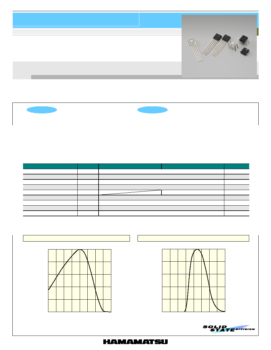
P H O T O I C
Light modulation photo IC
Fewer detection errors even under disturbance background light
S4282-51, S6809, S6846, S6986, S7136/-10
These light modulation photo ICs were developed for optical synchronous detection under disturbance background light. A photodiode,
preamplifier, comparator, oscillator, LED driver and signal processing circuit, etc. are all integrated on a monolithic photo IC chip. Optical
synchronous type photoreflectors and photointerrupters, which less susceptible to disturbance background light, can be easily configured by just
connecting an external LED to this photo IC. Our unique circuit design achieves an allowable background light level of 10000
lx
Typ. (S4282-51,
S6986) and a minimum detection level of 0.2 µW/mm
2
Typ. (S6846, S7136/-10).
s
Absolute maximum ratings (Ta=25
∞
C)
Parameter
Symbol
S4282-51, S6986
S6809, S6846, S7136/-10
Unit
Supply voltage
Vcc
-0.5 to +16V
Output voltage
Vo
-0.5 to +16
V
Output current
Io
50
mA
Cathode output voltage
Vcath
-0.5 to +16
V
Cathode output current
Icath
70
mA
Power dissipation *
1
P
250
mW
Operating temperature
Topr
-25 to +60
∞
C
Storage temperature
Tstg
-40 to +100
∞
C
Soldering
-
230
∞
C, 5 s, at least 1.8 mm away from package surface
-
*1: Derate power dissipation at a rate of 3.3 mW/∞C above Ta=25 ∞C
s
Spectral response (typical example)
400
600
800
1000
1200
WAVELENGTH (nm)
0
20
40
60
80
100
RELATIVE SENSITIVITY (%)
(Ta=25 ∞C)
400
600
800
1000
1200
0
20
40
60
80
100
(Ta=25 ∞C)
WAVELENGTH (nm)
RELATIVE SENSITIVITY (%)
KPICB0001EB
KPICB0002EA
S4282-51, S6986
S6809, S6846, S7136/-10
Light modulation photo IC
S4282-51, S6809, S6846, S6986, S7136/-10
s
Electrical and optical characteristics (Ta=25
∞
C, Vcc=5 V)
S4282-51, S6986
S6809, S6846, S7136 /-10
Output: built-in pull-up resistor *
2
Cathode: constant current drive
Output: open collector *
3
Cathode: open collector drive
Parameter
Symbol
Condition
Min.
Typ.
Max.
Min.
Typ.
Max.
Unit
Supply voltage
Vcc
4.5
-
164.5
-
16 V
Current
consumption
Icc
Vo, LED
terminals open
-
4
11
-
4
11
mA
Low level
output voltage
V
OL
I
OL
=16 mA
-
0.2
0.4
-
0.2
0.4
V
4.9
-
-
V
Out
p
ut
High level
output
voltage
V
OH
4.7 k
between
Vcc and Vo
4.9
-
-
V
Low level
output voltage Vcath Icath=40 mA
-
-
0.8
V
Low level
output current Icath Vcath=1.2 V
15
35
60
mA
Pulse cycle
Tp
65
130
220
65
130
220
µ
s
Cathode
Pulse width
Tw
4
8
13.7
4
8
13.7
µ
s
H
L
Threshold
light level
E
HL
=940 nm
No background light
-
0.7
2
-
0.2
1.0
µ
W/mm
2
0.45
0.65
0.95
Hysteresis
-
0.45
0.65
0.95
0.65
(S6809)
0.8
(S6809)
0.95
(S6809)
-
Frequency
response
f
0.5
1.25
-
0.5
1.25
-
kHz
Allowable
background
light level
Ex
Signal light: 5
µ
W /mm
p=940 nm
Background light:
A light source
5000
10000
-
2000
3000
-
l x
Vcc
CATHODE
(LED)
GND
Vcc
Vout
GND
Cathode
Output
10 k
*2:
*3:
Vcc
CATHODE
(LED)
GND
Vcc
Vout
GND
Cathode
Output
KPICC0009EA
KPICC0010EA
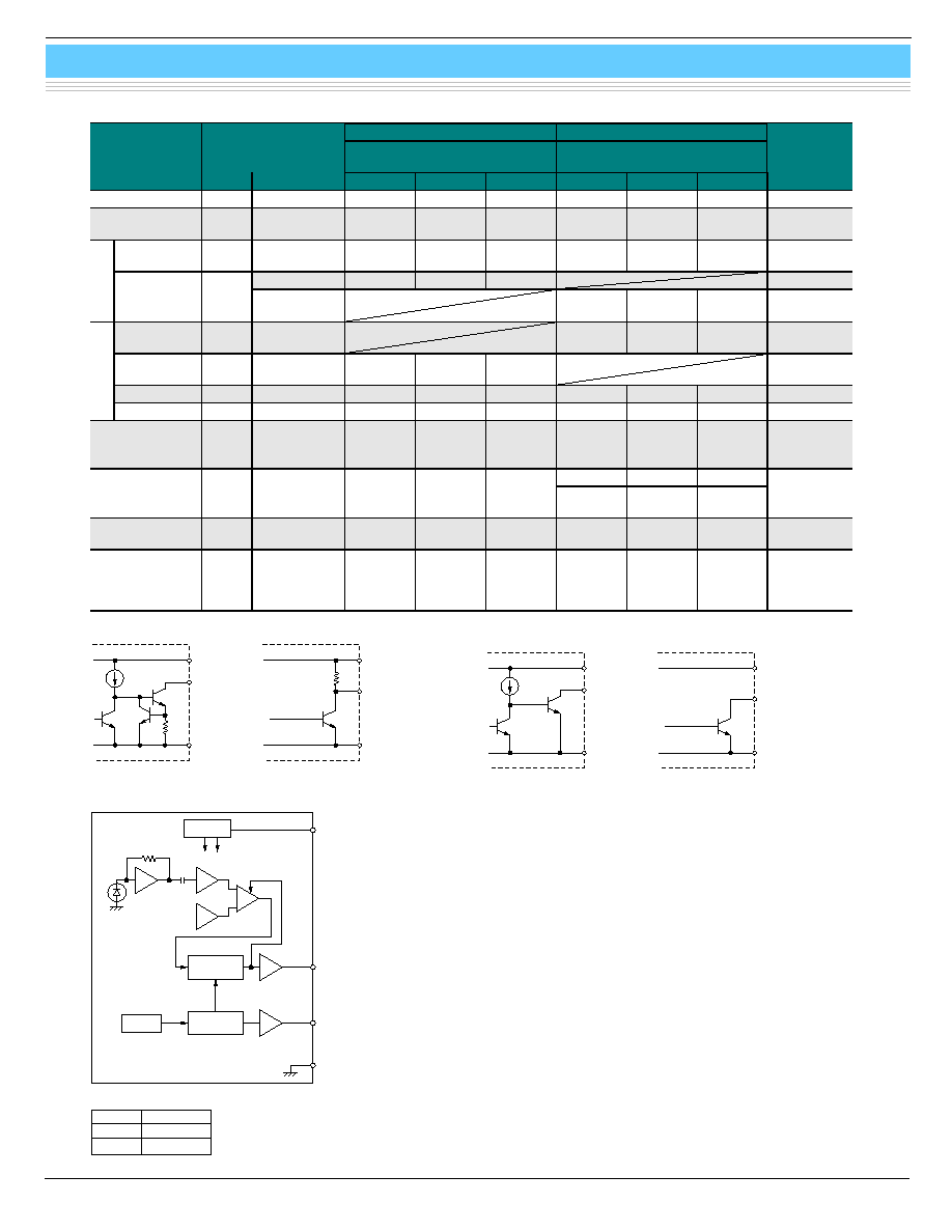
CONSTANT
VOLTAGE
BUFFER
SIGNAL
PROCESSING
CIRCUIT
TIMING
GENERATOR
OSCILLATOR
LED
DRIVER
OUTPUT
CIRCUIT
GND
CATHODE
(LED)
Vout
Vcc
COMPARATOR
PREAMP
PD
Vref
TRUTH TABLE
INPUT
OUTPUT LEVEL
LIGHT ON
LIGHT OFF
LOW
HIGH
s
Block diagram and internal functions
(a) Oscillator and timing signal generator
The oscillator produces a reference oscillation output by charging and discharging the
built-in capacitor with constant current. The oscillation output is fed to the timing signal
generator, which then creates LED drive pulses and various timing pulses for digital
signal processing.
(b) LED driver circuit
This circuit drives an external LED using the LED drive pulses created by the timing
signal generator. The duty cycle is 1/16.
(c) Photodiode and preamplifier circuit
The photodiode is formed on the same monolithic chip. A photocurrent generated in the
photodiode is converted to a voltage by a preamplifier circuit. The preamplifier circuit
uses an AC amplifier to expand the dynamic range versus DC or low-frequency
background light, without impairing signal detection sensitivity.
(d) Capacitive coupling, buffer amplifier and reference voltage generator
Capacitive coupling removes low-frequency noise and also cancels the DC offset in
the preamplifier. The buffer amplifier boosts the signal up to the comparator level, and
the reference voltage generator produces a comparator level voltage.
(e) Comparator circuit
The comparator circuit has a hysteresis function to prevent chattering caused by
small fluctuations in the input light.
(f) Signal processing circuit
The signal processing circuit consists of a gate circuit and digital integrator circuit. The
gate circuit discriminates input pulses during synchronous detection, to prevent op-
erational errors caused by asynchronous background light. Background light which is
synchronized with the signal detection timing cannot be eliminated by the gate circuit,
but is canceled out by the digital integrator circuit at the latter stage.
(g) Output circuit
This circuit serves as an output buffer for the signal processing circuit and outputs the
signal to an external circuit.
KPICC0002EA
Light modulation photo IC
S4282-51, S6809, S6846, S6986, S7136/-10
5.2 ± 0.3
(INCLUDING BURR)
CENTER OF
ACTIVE AREA
5.2 ± 0.3
(INCLUDING BURR)
(SPECIFIED AT THE LEAD ROOT)
PHOTOSENSITIVE
SURFACE
Vout
GND
CATHODE (LED)
Vcc
2.0
(DEPTH 0.15 MAX.)
1.0
(DEPTH 0.15 MAX.)
2.5 ± 0.2
5.0
2.05 ± 0.2
16.5 ± 1.0
(0.8)
(1.0)
1.27 1.27 1.27
10∞
5∞
0.7 ± 0.15
10
∞
5
∞
0.25
+0.15
-0.1
0.55
0.45
1.0
2.0
Tolerance unless otherwise
noted: ±0.1, ±2∞
Shaded area indicates burr.
Values in parentheses are not
guaranteed, but for reference.
5.0
KPICA0008EC
s
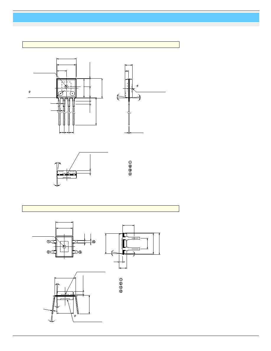
Dimensional outlines (unit: mm)
S6809, S6846, S6986
KPICA0009EB
S4282-51, S7136
0.5
4.6 ± 0.2
(INCLUDING BURR)
CENTER OF
ACTIVE AREA
4.5 *
0.7
3.1 ± 0.4
1.0
2.0
5.4 *
2.54
5.5
5.6
±
0.2
(INCLUDING BURR)
10
∞
3
∞
3∞
5∞
5.75 ± 0.2
0.7
±
0.15
PHOTOSENSITIVE
SURFACE
4.5
±
0.4
4.5 *
7.5 ± 5∞
0.25
CATHODE (LED)
Vcc
Vout
GND (SHORT LEAD)
Tolerance unless otherwise
noted: ±0.1, ±2∞
Shaded area indicates burr.
Chip position accuracy
with respect to the package
dimensions marked *
X
±0.2
Y
±0.2
2.0
(DEPTH 0.15 MAX.)

HAMAMATSU PHOTONICS K.K., Solid State Division
1126-1 Ichino-cho, Hamamatsu City, 435-8558 Japan, Telephone: (81) 053-434-3311, Fax: (81) 053-434-5184, http://www.hamamatsu.com
U.S.A.: Hamamatsu Corporation: 360 Foothill Road, P.O.Box 6910, Bridgewater, N.J. 08807-0910, U.S.A., Telephone: (1) 908-231-0960, Fax: (1) 908-231-1218
Germany: Hamamatsu Photonics Deutschland GmbH: Arzbergerstr. 10, D-82211 Herrsching am Ammersee, Germany, Telephone: (49) 08152-3750, Fax: (49) 08152-2658
France: Hamamatsu Photonics France S.A.R.L.: 8, Rue du Saule Trapu, Parc du Moulin de Massy, 91882 Massy Cedex, France, Telephone: 33-(1) 69 53 71 00, Fax: 33-(1) 69 53 71 10
United Kingdom: Hamamatsu Photonics UK Limited: 2 Howard Court, 10 Tewin Road, Welwyn Garden City, Hertfordshire AL7 1BW, United Kingdom, Telephone: (44) 1707-294888, Fax: (44) 1707-325777
North Europe: Hamamatsu Photonics Norden AB: Smidesv‰gen 12, SE-171 41 Solna, Sweden, Telephone: (46) 8-509-031-00, Fax: (46) 8-509-031-01
Italy: Hamamatsu Photonics Italia S.R.L.: Strada della Moia, 1/E, 20020 Arese, (Milano), Italy, Telephone: (39) 02-935-81-733, Fax: (39) 02-935-81-741
Information furnished by HAMAMATSU is believed to be reliable. However, no responsibility is assumed for possible inaccuracies or omissions.
Specifications are subject to change without notice. No patent rights are granted to any of the circuits described herein. ©2001 Hamamatsu Photonics K.K.
Light modulation photo IC
S4282-51, S6809, S6846, S6986, S7136/-10
Cat. No. KPIC1002E05
Feb. 2001 DN
S7136-10
KPICA0034EA
Tolerance unless otherwise noted: ±0.1
Shaded area indicates burr.
Chip position accuracy
with respect to package
dimensions marked *
X
±0.2
Y
±0.2
4.6 ± 0.2
(INCLUDING BURR)
CENTER OF
ACTIVE AREA
INDEX MARK
0.6
0.5
4.5 *
1.5 ± 0.4
1.5 ± 0.4
2.54
5.6 ± 0.2
(INCLUDING BURR)
5.4 *
10
∞
5.5 *
0.7 ± 0.15
1.0
2.0
7.5 ± 0.3
0.7 ± 0.3
0.7 ± 0.3
5∞
0.25
0.1 ± 0.1
3∞
3
∞
CATHODE (LED)
Vcc
Vout
GND
PHOTOSENSITIVE
SURFACE