 | –≠–ª–µ–∫—Ç—Ä–æ–Ω–Ω—ã–π –∫–æ–º–ø–æ–Ω–µ–Ω—Ç: S4581-06 | –°–∫–∞—á–∞—Ç—å:  PDF PDF  ZIP ZIP |

Hamamatsu offers a variety of 1-D PSDs (Position Sensitive Detectors) molded into plastic packages.
These PSDs feature excellent position detection resolution, high resistance to disturbance background light and high reliability.
Features
l Excellent position detection resolution
l High reliability
l Thin, miniature plastic package
l Clear package passing wide wavelength range or
visible-cut package reducing background light noise
l Surface mount package is available
l Suitable for high-speed, microscopic spot light:
S7879, S8361
l High sensitivity in the red region: S8361
l High interelectrode resistance: S3271 to S3274-05
S7105-05, S5629-02
Applications
l Camera auto focus
l Range finder
l Optical proximity switch
l Displacement meter
P S D
One-dimensional PSD
1-D PSD with plastic package
Plastic package
s
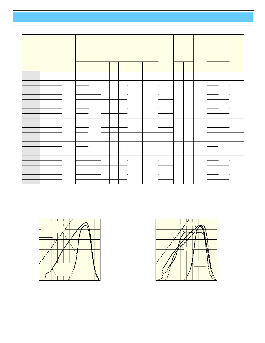
General ratings / Absolute maximum ratings
Absolute maximum ratings
Active area
Resistance
length
Reverse voltage
V
R
Max.
Operating
temperature
Topr
Storage
temperature
Tstg
Type No.
Dimensional
outline
(mm)(mm) (V) (∞C) (∞C)
S6407
1 ◊ 1
1
S6515
1 ◊ 1.2
1.2
S4580-04
S4580-06
0.8 ◊ 1.5
1.5
S4581-04
S4581-06
S3271-05
1 ◊ 2
2
S4582-04
S4582-06
S3272-05
1 ◊ 2.5
2.5
S4583-04
S4583-06
S3273-05
1 ◊ 3
3
S7879
S8361
1 ◊ 3
3
S4584-04
S4584-06
S3274-05
1 ◊ 3.5
3.5
S7105-04
S7105-06
S7105-05
1 ◊ 4.2
4.2
S5629
S5629-01
S5629-02
1 ◊ 6
6
20
-25 to +85
-40 to +100
NEW
NEW
1
One-dimensional PSD
Plastic package
200
400
800
1000
1200
WAVELENGTH (nm)
PHOTO SENSITIVITY
(A/W)
0.5
0.4
0.3
0.2
0.1
0
0.6
600
(Typ. Ta=25 ∞C)
S4580-06
S4582 to S4584-06
S7105-06
S5629-01
QE=100 %
S6407, S6515, S4580-04
S4582 to S4584-04,
S7105-04/-05, S5629/-02
S3272 to S3274-05
200
400
800
1000
1200
WAVELENGTH (nm)
PHOTO SENSITIVITY
(A/W)
0.5
0.4
0.3
0.2
0.1
0
0.6
600
(Typ. Ta=25 ∞C)
S4581-04
S3271-05
S7879
S4581-06
QE=100 %
S8361
KPSDB0079EB
s Spectral response
KPSDB0080EB
2
s
Electrical and optical characteristics (Typ. Ta=25 ∞C, unless otherwise noted)
Spectral
response
range
l
Peak
sensitivity
wavelength
lp
Photo
sensitivity
S
Interelectrode
resistance
Rie
Vb=0.1 V
Position
detection error *
V
R
=1 V
spot light size =B300µm
Saturation
photocurrent
*
Ist
V
R
=1 V
R
L
=1 k9
Dark
current
I
D
V
R
=1 V
Temp.
coefficient
of
I
D
T
CID
Rise time *
!
tr
V
R
=1 V
R
L
=1 kW
Terminal
capacitance
Ct
V
R
=1 V
f=10 kHz
Type No.
(nm)(nm)
l=650 nm
(A/W)
l=890 nm
(A/W)
Min.
(kW)
Typ.
(kW)
Max.
(kW)
Typ.
(µm)
Max.
(µm)(µA)
Typ.
(nA)
Max.
(nA) (Times/∞C)
l=650 nm
(µs)
l=890 nm
(µs)
(pF)
S6407
160 200 240
25
S6515
760 to 1100 960
-
0.51 100 140 180 ±5
±15
30
0.05
1
1.15
-
10
15
S4580-04 760 to 1100
-
-
S4580-06 320 to 1100 960
0.35 0.51 100 140 180
±10
±20
30
0.05
1
1.15
3
10
15
S4581-04 760 to 1060
-
0.51
-
S4581-06 320 to 1060
0.38 0.53 100 140 180
30
3
10
S3271-05 760 to 1060
920
-
0.51 320 400 480
±10
±20
15
0.05
1
1.15
-
15
15
S4582-04 760 to 1100
-
-
S4582-06 320 to 1100
0.33
100 140 180
30
3
10
S3272-05 760 to 1100
960
-
0.51
320 400 480
±10
±25
15
0.05
1
1.15
-
15
15
S4583-04 760 to 1100
-
-
S4583-06 320 to 1100
0.33
100 140 180
30
3
10
S3273-05 760 to 1100
-
320 400 480
±10
±30
15
-
15
15
S7879
440 to 1100
960
0.36
0.51
S8361
400 to 1100 680
0.45 0.45 70 110 150
±15
±60
40
0.05
1
1.15
1
4
30
S4584-04 760 to 1100
-
-
S4584-06 320 to 1100
0.33
100 140 180
30
3
10
S3274-05 760 to 1100
960
-
0.51
320 400 480
±15
±35
15
0.05
1
1.15
-
15
15
S7105-04 760 to 1100
-
0.51
-
S7105-06 320 to 1100
0.38 0.55 100 140 180
30
2
5
S7105-05 760 to 1100
960
-
0.51 320 400 480
±15
±40
15
0.1
2
1.15
-
10
40
S5629
760 to 1100
-
0.51
-
S5629-01 320 to 1100
0.38 0.55 30 50 80
80
2
5
S5629-02 760 to 1100
960
-
0.51 240 300 360
±20
±60
20
0.1
2
1.15
-
10
60
*1: In the range 75 % from the center of the active area to the edge.
*2: This indicates the upper limit of the photocurrent linearity over the entire incident light quantity and is defined as the
photocurrent at a point where the linearity deviates by 10 %.
*3: Time required for output change from 10 to 90 % of the steady output value when stepped function light is input to the PSD.
One-dimensional PSD
Plastic package
WAVELENGTH (nm)
TEMPERATURE COEFFICIENT
(%/
∞
C)
+1.5
+1.0
+0.5
0
-0.5
200
600
1000
1200
800
400
(Typ.)
POSITION ON PSD (mm)
+1.5
0
-1.5
+50
0
-50
-1.5
-1.0
-0.5
+0.5
+1.0
0
+1.5
POSITION ON PSD (mm)
0
0.5
1.0
RELATIVE PHOTOCURRENT OUTPUT
POSITION DETECTION ERROR (µm)
I
2
I
1
OUTPUT I
1
L (RESISTANCE LENGTH)
INCIDENT LIGHT
OUTPUT I
2
1 nA
100 pA
10 pA
0.01
0.1
1
10
100
REVERSE VOLTAGE (V)
DARK CURRENT
1 pA
(Typ. Ta=25 ∞C)
S6407, S6515
S4580-04/-06
S4582 to S4584-04/-06
S7105-04/-05/-06
S3272 to S3274-05
S5629/-01/-02
S7879, S8361
S4581-04/-06, S3271-05
10
100
1000
(Typ. Ta=25 ∞C)
INTERELECTRODE RESISTANCE (k
)
SATURATION PHOTOCURRENT
1 mA
100 µA
10 µA
1 µA
V
R
= 5 V
V
R
= 2 V
V
R
= 1 V
V
R
= 0 V
s Dark current vs. reverse voltage
s Saturation photocurrent vs.
interelectrode resistance
s Position detection characteristic example
(S4583-04, active area size: 1 ◊ 3 mm)
s Definition of position detection error
When the electrical center of a PSD is assumed to be the
position of incident light where light current I
1
equals I
2
,
position detection error at each incident position can be
defined by the following equation.
KPSDB0005EB
KPSDC0001EA
The electrical center is viewed as 0, I
1
as (+), and I
2
as (-).
Position detection error (µm) = Incident position
-
KPSDB0002EE
s Photo sensitivity temperature
characteristic (S4581-06)
KPSDB0004EE
KPSDB0003EA
I
2
- I
1
L
I
1
+ I
2
2
◊
s Rise time vs. reverse voltage
KPSDB0095EA
KPSDB0096EB
REVERSE VOLTAGE (V)
(Typ. Ta=25 ∞C,
=650 nm)
RISE TIME (µs)
1
0.1
0
1
3
2
10
100
S4583-06
S7879, S8361
REVERSE VOLTAEG (V)
(Typ. Ta=25 ∞C,
=890 nm)
RISE TIME (µs)
1
0.1
0
10
8
6
4
2
10
100
S4583-06
S7879, S8361
3

One-dimensional PSD
Plastic package
s Dimensional outlines [unit: mm, tolerance unless otherwise noted: ±0.1, chip position accuracy (without ) with
respect to the package dimensions marked * X, Y
±0.2, ±2∞]
KPSDA0057EA
KPSDA0063EA
S6407, S6515 (Surface mounting type)
S3271 to S3274-05
5.0 ± 0.2
(INCLUDING BURR)
4.7 *
10
∞
4.8 *
5
∞
0.5
0.6
2.54
1.5 ± 0.4
1.5 ± 0.4
1.8
0.8
ANODE 1
CATHODE (COMMON)
ANODE 2
CATHODE (COMMON)
10∞
5∞
7.0 ± 0.3
0.7 ± 0.3
0.7 ± 0.3
0.25
0.1 ± 0.1
PHOTOSENSITIVE
SURFACE
4.0 *
4.1 ± 0.2
(INCLUDING BURR)
KPSDA0022EA
S4580 to S4584-04/-06 (Surface mounting type)
7.0 ± 0.3
0.7 ± 0.3
0.7 ± 0.3
0.25
0.1 ± 0.1
5∞
10∞
7.9 ± 0.3
X=3.0 ± 0.1
Y
±0.1
REFERENCE
HOLE
±2∞
4.1 ± 0.2
(INCLUDING BURR)
6.0 ± 0.06
1.77
1.95 ± 0.4
1.5 ± 0.4
1.5 ± 0.4
1.95 ± 0.4
4.0
1.77
0.5
1.905
1.905 REFERENCE
HOLE 0.9
-0
+0.06
R0.4
-0
4.7
5.0 ± 0.2
(INCLUDING BURR)
1.8
0.8
10
∞
0.5
Chip position accuracy with respect to
center of reference hole
5
∞
4.8
0.8
-0
+0.03
+0.06
PHOTOSENSITIVE
SURFACE
ANODE 1
CATHODE (COMMON)
NC
ANODE 2
CATHODE (COMMON)
CATHODE (COMMON)
RESISTANCE LENGTH
ANODE 1
ANODE 2
4
ANODE 1
CATHODE (COMMON)
ANODE 2
CATHODE (COMMON)
4.1 ± 0.2
(INCLUDING BURR)
4.0 *
4.9 ± 0.4
4.9 ± 0.4
(1.25)
(1.25)
13.8 ± 0.3
(0.8)
0.6
0.5
5.0 ± 0.2
(INCLUDING BURR)
0.3 MAX.
0.3 MAX.
10∞
0.8
0.25
1.8
5∞
4.7 *
10
∞
4.8 *
5
∞
2.54
(0.8)
0.5
PHOTOSENSITIVE
SURFACE
KPSDA0052EA
S7879, S8361
ANODE 1
CATHODE (COMMON)
ANODE 2
CATHODE (COMMON)
4.1 ± 0.2
(INCLUDING BURR)
4.0 *
5.2 ± 0.2
5.0 ± 0.2
(INCLUDING BURR)
4.5 ± 0.4
10∞
0.8
0.25
1.8
5∞
7.5∞ ± 5∞
4.7 *
10
∞
4.8 *
2.54
5
∞
0.5
PHOTOSENSITIVE
SURFACE
0.6
0.5
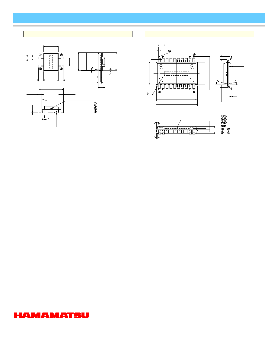
One-dimensional PSD
Plastic package
HAMAMATSU PHOTONICS K.K., Solid State Division
1126-1 Ichino-cho, Hamamatsu City, 435-8558 Japan, Telephone: (81) 053-434-3311, Fax: (81) 053-434-5184, http://www.hamamatsu.com
U.S.A.: Hamamatsu Corporation: 360 Foothill Road, P.O.Box 6910, Bridgewater, N.J. 08807-0910, U.S.A., Telephone: (1) 908-231-0960, Fax: (1) 908-231-1218
Germany: Hamamatsu Photonics Deutschland GmbH: Arzbergerstr. 10, D-82211 Herrsching am Ammersee, Germany, Telephone: (49) 08152-3750, Fax: (49) 08152-2658
France: Hamamatsu Photonics France S.A.R.L.: 8, Rue du Saule Trapu, Parc du Moulin de Massy, 91882 Massy Cedex, France, Telephone: 33-(1) 69 53 71 00, Fax: 33-(1) 69 53 71 10
United Kingdom: Hamamatsu Photonics UK Limited: 2 Howard Court, 10 Tewin Road, Welwyn Garden City, Hertfordshire AL7 1BW, United Kingdom, Telephone: (44) 1707-294888, Fax: (44) 1707-325777
North Europe: Hamamatsu Photonics Norden AB: Smidesv‰gen 12, SE-171 41 Solna, Sweden, Telephone: (46) 8-509-031-00, Fax: (46) 8-509-031-01
Italy: Hamamatsu Photonics Italia S.R.L.: Strada della Moia, 1/E, 20020 Arese, (Milano), Italy, Telephone: (39) 02-935-81-733, Fax: (39) 02-935-81-741
Information furnished by HAMAMATSU is believed to be reliable. However, no responsibility is assumed for possible inaccuracies or omissions.
Specifications are subject to change without notice. No patent rights are granted to any of the circuits described herein. ©2001 Hamamatsu Photonics K.K.
Cat. No. KPSD1009E05
Dec. 2001 DN
0.35
0.45
0.89
5.2 *
(INCLUDING BURR)
5.4 ± 0.2
8.0 ± 0.3
1.4 ± 0.3
1.4 ± 0.3
1.0
9.5 *
9.7 ± 0.2
(INCLUDING BURR)
15
∞
10
∞
0.1 ± 0.1
0.2
0.5
0.8
1.7
15∞
10∞
PHOTOSENSITIVE
SURFACE
ANODE 1
CATHODE (COMMON)
ANODE 2
CATHODE (COMMON)
NC (SHORT LEAD)
NC (SHORT LEAD)
0.6 ± 0.3
0.6 ± 0.3
to
to
KPSDA0023EA
S5629/-01/-02 (Surface mounting type)
5
4.6 ± 0.2
(INCLUDING BURR)
0.6
0.5
4.5 *
1.5 ± 0.4
1.5 ± 0.4
2.54
5.6 ± 0.2
(INCLUDING BURR)
5.4 *
10
∞
5.5 *
0.7
1.0
2.0
7.5 ± 0.3
0.7 ± 0.3
0.7 ± 0.3
5∞
0.25
0.1 ± 0.1
3∞
3
∞
ANODE 1
CATHODE (COMMON)
ANODE 2
CATHODE (COMMON)
PHOTOSENSITIVE
SURFACE
KPSDA0047EA
S7105-04/-05/-06 (Surface mounting type)