 | –≠–Ľ–Ķ–ļ—ā—Ä–ĺ–Ĺ–Ĺ—č–Ļ –ļ–ĺ–ľ–Ņ–ĺ–Ĺ–Ķ–Ĺ—ā: S4810 | –°–ļ–į—á–į—ā—Ć:  PDF PDF  ZIP ZIP |
S4810 and S6289 are digital output photo ICs consisting of a photodiode, schmitt trigger circuit and output transistor, all integrated on a single chip and
molded into a visible-cut, subminiature plastic package.
Features
l Low-voltage operation: 2.2 to 7 V
l Subminiature plastic package with lens
l Low current consumption
l Open collector output
l S4810: "H" level output at light input
S6289: "L" level output at light input
Applications
l Cameras
l Tape start/end mark sensor for VTRs, cassette tape
recorders, etc.
l Optical switches
l Encoders
P H O T O I C
Low-voltage operation photo IC
Operation at low voltage from 2.2 V
S4810, S6289
s
Absolute maximum ratings (Ta=25 įC)
Parameter
Symbol
Value
Unit
Supply voltage
Vcc
-0.5 to +7
V
Output voltage
Vo
-0.5 to +7
V
Output current
Io
8
mA
Power dissipation
P
150
mW
Operating temperature
Topr
-25 to +85
įC
Storage temperature
Tstg
-40 to +100
įC
Soldering
-
260 įC, 3 s, at least 2.5 mm away from package surface
-
s
Electrical and optical characteristics (Ta=25 įC, Vcc=5 V, light source: p=890 nm LED, unless otherwise noted)
S4810
S6289
Parameter
Symbol
Condition
Min.
Typ.
Max.
Min.
Typ.
Max.
Unit
Supply voltage
Vcc
2.2
-7.0
2.2
-7.0
V
Low level output voltage
V
OL
I
OL
=4 mA *
1
-
-
0.4
-
-
0.4
V
High level output current
I
OH
V
O
=5 V *
2
--10
--10
ĶA
Current consumption
I
CC
-
1.3
3
-
1.3
3
mA
LH Threshold illuminance
E
LH
R
L
=1.2 k
--1.5
---
ĶW/mm
2
HL Threshold illuminance
E
HL
R
L
=1.2 k
-
-
-
-
-
1.5
ĶW/mm
2
Hysterisis
-*
3
-0.9
- -0.85
- -
LH Propagation delay time
t
PLH
-
-
10
-
-
15
Ķs
HL Propagation delay time
t
PHL
--15
--10
Ķs
Rise time
tr
-
0.07
-
-
0.07
-
Ķs
Fall time
tf
2 ĶW/mm
2
R
L
=1.2 k
-0.03
- -0.03
- Ķs
Peak sensitivity wavelength
p
-
850
-
-
850
-
nm
*1: S4810: E (illuminance) =0 ĶW/mm
2
, S6289: E=2 ĶW/mm
2
*2: S4810: E=2 ĶW/mm
2
, S6289: E=0 ĶW/mm
2
*3: S4810: E
HL
/E
LH
, S6289: E
LH
/E
HL
Note) Connect a 0.01 ĶF capacitor or larger between Vcc and GND.
Low-voltage operation photo IC
S4810, S6289
(Typ. Ta=25 įC)
WAVELENGTH (nm)
RELATIVE SENSITIVITY (
%
)
100
80
60
40
20
0
600
700
800
900
1000
1100
1200
(Typ. Vcc=5 V, normalized at Ta=25 įC, L
ģH)
2.0
1.5
1.0
0.5
0
0
1
2
3
4
5
6
7
8
SUPPLY VOLTAGE (V)
THRESHOLD ILLUMINANCE (RELATIVE VALUE)
L
ģH -25 įC
H
ģL -25 įC
L
ģH 25 įC
H
ģL 25 įC
L
ģH 85 įC
H
ģL 85 įC
I
F
PULSE INPUT
5 V
Vo
GND
R
L
0.01
mF
I
F
t
PHL
tf
tr
V
OL
10 %
1.5 V
90 %
V
OH
50 %
t
PLH
s
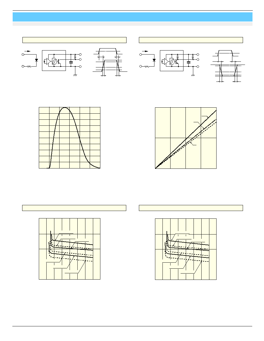
Spectral response
KPICB0004EB
s
Low level output voltage vs. low level output current
KPICB0005EA
KPICC0038EA
S6289
s
Threshold illuminance vs. supply voltage
KPICB0006EA
KPICB0046EA
S6289
S4810
(Typ. Vcc=5 V, normalized at Ta=25 įC, H
ģL)
2.0
1.5
1.0
0.5
0
0
1
2
3
4
5
6
7
8
SUPPLY VOLTAGE (V)
THRESHOLD ILLUMINANCE (RELATIVE VALUE)
H
ģL -25 įC
L
ģH -25 įC
H
ģL 25 įC
L
ģH 25 įC
H
ģL 85 įC
L
ģH 85 įC
7 V
5 V
2.2 V
0.2
0
LOW LEVEL OUTPUT CURRENT (mA)
LOW LEVEL OUTPUT VOLTAGE (V)
0.1
0
5
10
15
20
(Typ. Ta=25 įC)
I
F
PULSE INPUT
5 V
Vo
GND
R
L
0.01 ĶF
I
F
t
PLH
Vo
tr
tf
V
OL
10 %
1.5 V
90 %
V
OH
50 %
t
PHL
s
Response time measurement circuit
KPICC0005EA
S4810

Low-voltage operation photo IC
S4810, S6289
7 V
2.2 V
2.0
1.5
1.0
0.5
-50
0
50
100
AMBIENT TEMPERATURE (įC)
SUPPLY CURRENT (mA)
(Typ. E=0/2 ĶW/mm
2
)
5 V
LOW LEVEL
HIGH LEVEL
40
30
20
10
0
0
1
2
3
4
5
ENERGY DENSITY (
Ķ
W/mm
2
)
PROPAGATION DELAY TIME (Ķs)
(Typ. Ta=25 įC, Vcc=2.2 V to 7 V, R
L
=1.2 k
W)
S4810: L
ģH
S6289: H
ģL
S4810: H
ģL
S6289: L
ģH
s
Supply current vs. ambient temperature
KPICB0007EA
s
Low level output voltage vs. ambient temperature
KPICB0008EA
s
Threshold illuminance vs. ambient temperature
KPICB0009EA
s
Propagation delay time vs. input light strength
KPICB0010EB
s
Rise/fall time vs. load resistance
KPICB0011EB
s
Directivity
KPICB0012EA
(Typ. I
OL
=4 mA)
2.2 V
7 V
50
40
30
20
-50
0
50
100
AMBIENT TEMPERATURE (įC)
LOW LEVEL OUTPUT VOLTAGE (mV)
5 V
S4810: L
ģH
S6289: H
ģL
1.5
1
0.5
0.5
-50
0
50
100
AMBIENT TEMPERATURE (įC)
THRESHOLD ILLUMINANCE (RELATIVE VALUE)
S4810: H
ģL
S6289: L
ģH
(Typ. V
CC
=5 V, normalized at Ta=25 įC, S4810: L
ģH, S6289: LģH)
600
500
400
100
0
0.1
LOAD RESISTANCE (k
9)
RISE/FALL TIME (ns)
(Typ. Ta=25 įC, V
CC
=2.2 to 7 V, E=2 ĶW/mm
2
)
1
200
300
10
FALL TIME
RISE TIME
-
40į
-
50į
-
80į
-
70į
-
60į
-
90į
-
20į
-
30į
-
10į
0į
20į
30į
60
20
0
60
40
20
40
10į
RELATIVE SENSITIVITY
40į
50į
80į
70į
60į
90į
(Typ.)
40 %
60 %
80 %
100 %
20 %
HAMAMATSU PHOTONICS K.K., Solid State Division
1126-1 Ichino-cho, Hamamatsu City, 435-8558 Japan, Telephone: (81) 053-434-3311, Fax: (81) 053-434-5184, http://www.hamamatsu.com
U.S.A.: Hamamatsu Corporation: 360 Foothill Road, P.O.Box 6910, Bridgewater, N.J. 08807-0910, U.S.A., Telephone: (1) 908-231-0960, Fax: (1) 908-231-1218
Germany: Hamamatsu Photonics Deutschland GmbH: Arzbergerstr. 10, D-82211 Herrsching am Ammersee, Germany, Telephone: (49) 08152-3750, Fax: (49) 08152-2658
France: Hamamatsu Photonics France S.A.R.L.: 8, Rue du Saule Trapu, Parc du Moulin de Massy, 91882 Massy Cedex, France, Telephone: 33-(1) 69 53 71 00, Fax: 33-(1) 69 53 71 10
United Kingdom: Hamamatsu Photonics UK Limited: 2 Howard Court, 10 Tewin Road, Welwyn Garden City, Hertfordshire AL7 1BW, United Kingdom, Telephone: (44) 1707-294888, Fax: (44) 1707-325777
North Europe: Hamamatsu Photonics Norden AB: Smidesvšgen 12, SE-171 41 Solna, Sweden, Telephone: (46) 8-509-031-00, Fax: (46) 8-509-031-01
Italy: Hamamatsu Photonics Italia S.R.L.: Strada della Moia, 1/E, 20020 Arese, (Milano), Italy, Telephone: (39) 02-935-81-733, Fax: (39) 02-935-81-741
Information furnished by HAMAMATSU is believed to be reliable. However, no responsibility is assumed for possible inaccuracies or omissions.
Specifications are subject to change without notice. No patent rights are granted to any of the circuits described herein. ©2001 Hamamatsu Photonics K.K.
Low-voltage operation photo IC
S4810, S6289
Cat. No. KPIC1005E03
Mar. 2001 DN
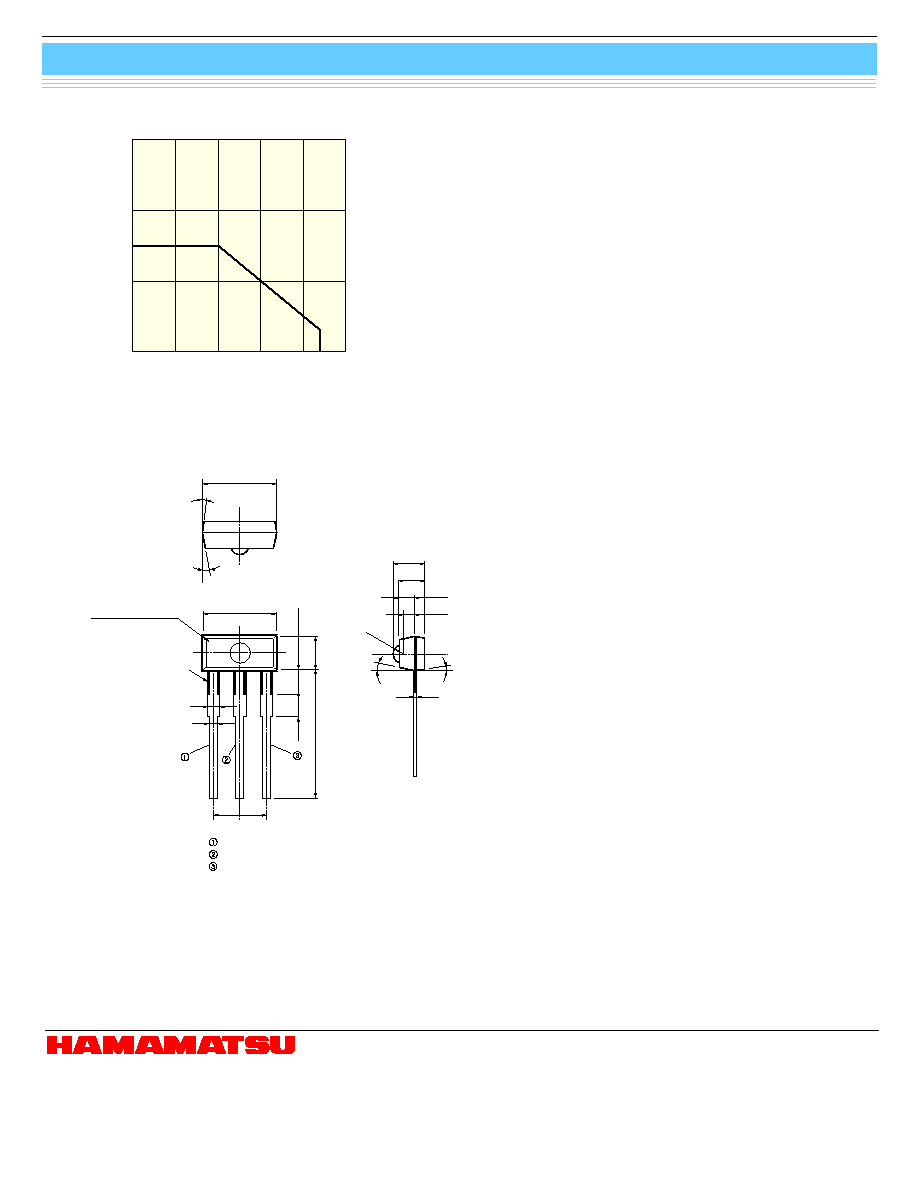
3.5
5į
10į
VISIBLE-CUT RESIN
(BLACK)
3.5
0.6
0.4
(SPECIFIED AT THE LEAD ROOT)
(1.0)
(1.15)
1.6
6.0 Ī 1.0
1.3
1.6
0.72
0.57
0.16
R0.45
10į
5į
Tolerance unless otherwise
noted: Ī0.2, Ī2į
Shaded area indicates burr.
Values in parentheses are not
guaranteed, but for reference.
V
O
GND
Vcc
BURR
1.27 1.27
s
Dimensional outline (unit: mm)
AMBIENT TEMPERATURE (įC)
POWER DISSIPATION (mW)
0
-25
0
25
50
75
100
300
100
200
(Typ.)
s
Power dissipation vs. ambient temperature
KPICB0048EA
KPICA0005EB