Features
l Miniature plastic package with lens
l Transistor output with built-in pull-up resistor
l S4825: "H" level output at light input
S4826: "L" level output at light input
Applications
l Paper detection in printers and copiers, etc.
l Optical switches
l Rotary encoders
P H O T O I C
Photo IC
Miniature package photo IC
S4825, S4826
S4825 and S4826 are digital output photo ICs consisting of a high-sensitivity photodiode, an amplifier, a schmitt trigger circuit and an output
transistor, all integrated on one chip molded into a miniature visible-cut plastic package.
s
Absolute maximum ratings (Ta=25 ∞C)
Parameter
Symbol
Value
Unit
Supply voltage
Vcc
-0.5 to +12
V
Output voltage
Vo
-0.5 to Vcc
V
Low level output current
Io Max.
50
mA
Power dissipation
P
300
mW
Operating temperature
Topr
-25 to +85
∞C
Storage temperature
Tstg
-40 to +100
∞C
Soldering
-260 ∞C, 3 s, at least 2.5 mm away from package surface
-
s
Electrical and optical characteristics (Ta=25 ∞C, Vcc=5 V, light source: p=950 nm LED, unless otherwise noted)
S4825
S4826
Parameter
Symbol
Condition
Min.
Typ.
Max.
Min.
Typ.
Max.
Unit
Supply voltage
Vcc
4.5
-12
4.5
-12
V
Low level output voltage
V
OL
I
OL
=16 mA *
1
-
0.1
0.4
-
0.1
0.4
V
High level output voltage
V
OH
Vo=5 V *
2
4.9
--4.9
--
V
Low level current consumption
I
CCL
*
1
-
5.6
12
-
5.4
12
mA
High level current consumption
I
CCH
*
2
-3.2
10
-3.6
10
mA
LH Threshold illuminance
E
LH
R
L
=280
-
1
3
-
-
-
µW/mm
2
HL Threshold illuminance
E
HL
R
L
=280
-
-
-
-
1
3
µW/mm
2
Hysterisis
-
*
3
-
0.9
-
-
0.9
-
-
LH Propagation delay time
t
PLH
-2.0
9
-4.5
15
µs
HL Propagation delay time
t
PHL
-
3.5
15
-
1.0
9
µs
Rise time
tr
-0.15
- -0.15
-
µs
Fall time
tf
E=8 µW/mm
2
R
L
=280
-
0.03
-
-
0.03
-
µs
Peak sensitivity wavelength
p
-850
- -850
-
nm
*1: S4825: E (illuminance) =0 µW/mm
2
, S4826: E=8 µW/mm
2
*2: S4825: E=8 µW/mm
2
, S4826: E=0 µW/mm
2
*3: S4825: E
HL
/E
LH
, S4826: E
LH
/E
HL
Note) Connect a 0.01 µF capacitor or larger between Vcc and GND.
HAMAMATSU PHOTONICS K.K., Solid State Division
1126-1 Ichino-cho, Hamamatsu City, 435-8558 Japan, Telephone: (81) 053-434-3311, Fax: (81) 053-434-5184, http://www.hamamatsu.com
U.S.A.: Hamamatsu Corporation: 360 Foothill Road, P.O.Box 6910, Bridgewater, N.J. 08807-0910, U.S.A., Telephone: (1) 908-231-0960, Fax: (1) 908-231-1218
Germany: Hamamatsu Photonics Deutschland GmbH: Arzbergerstr. 10, D-82211 Herrsching am Ammersee, Germany, Telephone: (49) 08152-3750, Fax: (49) 08152-2658
France: Hamamatsu Photonics France S.A.R.L.: 8, Rue du Saule Trapu, Parc du Moulin de Massy, 91882 Massy Cedex, France, Telephone: 33-(1) 69 53 71 00, Fax: 33-(1) 69 53 71 10
United Kingdom: Hamamatsu Photonics UK Limited: 2 Howard Court, 10 Tewin Road, Welwyn Garden City, Hertfordshire AL7 1BW, United Kingdom, Telephone: (44) 1707-294888, Fax: (44) 1707-325777
North Europe: Hamamatsu Photonics Norden AB: Smidesv‰gen 12, SE-171 41 Solna, Sweden, Telephone: (46) 8-509-031-00, Fax: (46) 8-509-031-01
Italy: Hamamatsu Photonics Italia S.R.L.: Strada della Moia, 1/E, 20020 Arese, (Milano), Italy, Telephone: (39) 02-935-81-733, Fax: (39) 02-935-81-741
Information furnished by HAMAMATSU is believed to be reliable. However, no responsibility is assumed for possible inaccuracies or omissions.
Specifications are subject to change without notice. No patent rights are granted to any of the circuits described herein. ©2001 Hamamatsu Photonics K.K.
Photo IC
S4825, S4826
Cat. No. KPIC1033E01
Mar. 2001 DN
4.3 ± 0.3
(INCLUDING BURR)
4.15
3.0
2.4
R 0.9
0.45
0.6
10∞
5∞
10∞
5∞
0.45
(SPECIFIED AT THE LEAD ROOT)
0.6 ± 0.3
(0.8)
(1.2)
1.43
4.43
15 MIN.
1.4
1.7
(INCLUDING BURR)
4.6
+0.6 -0.3
GND
V
O
Vcc
Tolerance unless otherwise
noted: ±0.2, ±2∞
Shaded area indicates burr.
Values in parentheses are not
guaranteed, but for reference.
1.27 1.27
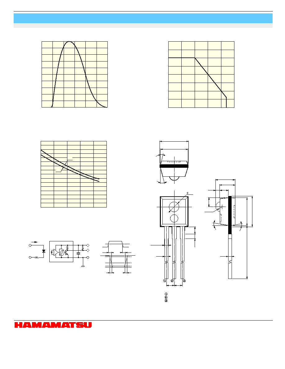
s
Power dissipation vs. ambient temperature
s
Threshold illuminance vs. ambient temperature (S4826)
KPICB0031EA
s
Dimensional outline (unit: mm)
s
Response time measurement circuit (S4826)
KPICC0038EA
(Typ. Ta=25 ∞C)
1200
1000
800
600
0
WAVELENGTH (nm)
RELA
TIVE SENSITIVITY (%)
20
40
60
80
100
POWER DISSIPATION (mW)
AMBIENT TEMPERATURE (∞C)
400
300
200
100
0
-25
0
25
50
75
100
KPICB0028EA
KPICB0047EA
-25
AMBIENT TEMPERATURE (∞C)
THRESHOLD ILLUMINANCE (RELATIVE VALUE)
0
0.2
0.4
0.6
0.8
1
1.2
1.4
1.6
(Typ. Ta=25 ∞C, Vcc=5 V, E
HL
=1.0)
0
25
50
75
100
E
HL
E
LH
I
F
PULSE INPUT
5 V
Vo
GND
R
L
0.01
mF
I
F
t
PHL
tf
tr
V
OL
10 %
1.5 V
90 %
V
OH
50 %
t
PLH
KPICA0022EA
s
Spectral response