 | –≠–ª–µ–∫—Ç—Ä–æ–Ω–Ω—ã–π –∫–æ–º–ø–æ–Ω–µ–Ω—Ç: S5590 | –°–∫–∞—á–∞—Ç—å:  PDF PDF  ZIP ZIP |

S5590, S5591
S5590, S5591 are low-noise light sensors consisting of a large area Si photodiode, op amp, and feedback resistance and capacitance, all
integrated into a small package. By simply connecting to a power supply, S5590 and S5591 can be used in low-light-level measurement such as
spectrophotometry.
Features
l
Si photodiode for UV to near IR precision photometry
l
Small package with quartz window
S5590: TO-5
S5591: TO-8
l
FET input operational amplifier with low power
dissipation
l
Built-in Rf=1 G
and Cf=5 pF
l
Variable gain with an externally connected resistor
l
Low noise and NEP
l
Guard ring structure for low level signal
Applications
l
Spectrophotometry
l
General-purpose optical measurement
P H O T O D I O D E
Si photodiode with preamp
Photodiode and preamp integrated with feedback resistance and capacitance
s General ratings / Absolute maximum ratings
Absolute maximum ratings
Active area
size
Package
Number
of
terminals
Supply
voltage
(op amp)
Vcc
Reverse
voltage
(ph ot o dio d e)
V
R
Power
dissipation
P
Operating
temperature
Topr
Storage
temperature
Tstg
Type No.
Dimensional
outline/
Window
material *
(mm)
(V)
(V)
(mW)
(∞C)
(∞C)
S5590
/Q
2.4 ◊ 2.4
TO-5
10
S5591
/Q
5.8 ◊ 5.8
TO-8
12
±18
5
500
-20 to +60
-30 to +80
s Electrical and optical characteristics (Typ. Ta=25 ∞C, Vcc=±15 V, R
L
=1 M
, unless otherwise noted)
S p e ctral
res p o n s e
ran g e
Peak
sensitivity
wavelength
p
Feedback
resistance
Rf
(built-in)
Feedback
capacitance
Cf
(built-in)
Photo
sensitivity
S
(V/nW)
Output
noise
voltage
Vn
Dark state
f=10 Hz
Noise
equivalent
power
NEP
=
p
(fW/Hz
1/2
)
Output
offset
voltage
Vos
Dark state
Cut-off
frequency
fc
Supply
current
Is
Dark state
Type No.
(nm)
(nm)
(G
)
(pF)
=200
nm
=
p
(µVrms/Hz
1 /2
)
f=10 Hz f=20 Hz
(mV)
(MHz)
(mA)
S5590
7
15
15
S5591
190 to
1100
960
1
5
-0.12 -0.52
8
16
17
±2
32
0.6
* Window material Q: quartz glass
1

Si photodiode with preamp
S5590, S5591
NEP (f,
) =
=
∑∑∑ (1)
Vn (f)
G
I - V (f)
∑ Ssi (
)
NEP (f,
p) ∑ S (
p)
S (
)
KSPDB0093EA
KSPDB0045EC
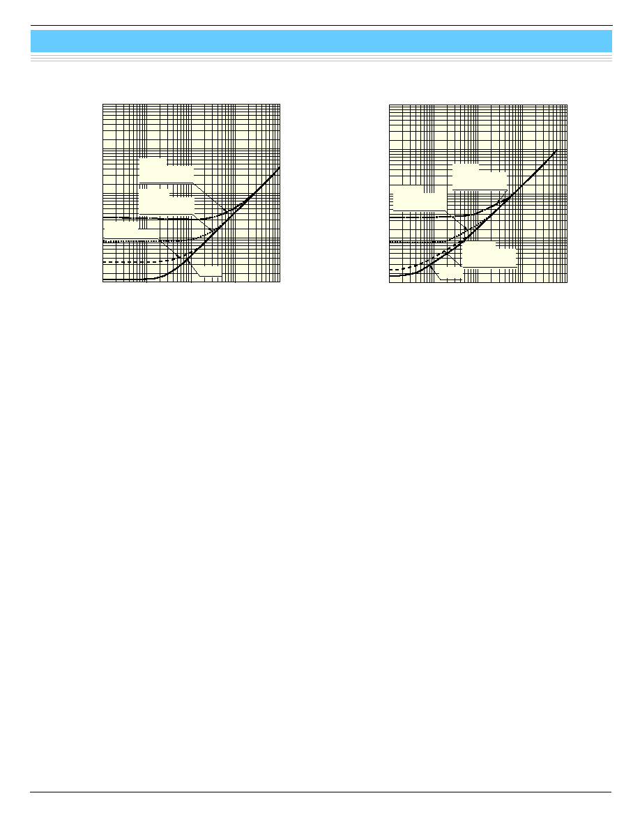
Figure 3 Output noise voltage vs. frequency (S5590)
KSPDB0066EA
0.01
0.1
1
CURRENT-TO-VOLTAGE
CONVERSION GAIN (M
)
FREQUENCY (kHz)
10
100
[Typ. Ta=25 ∞
C, Vcc=±15 V, Cf=5 pF (built-in), R
L
=1 M
]
10
-2
10
-1
10
0
10
1
10
2
10
3
10
4
+1 M
(EXTERNALLY
CONNECTED)
+11 M
(EXTERNALLY
CONNECTED)
+111 M
(EXTERNALLY
CONNECTED)
S5590, S5591
0.01
0.01
0.1
1
OUTPUT NOISE
VOLTAGE (
µ
Vrms/Hz
1/2
)
FREQUENCY (kHz)
10
100
0.1
1
100
[Typ. Ta=25 ∞C, Vcc=±15 V, Cf=5 pF (built-in), R
L
=1 M
, dark state]
10
+1 M
(EXTERNALLY
CONNECTED)
+11 M
(EXTERNALLY
CONNECTED)
+111 M
(EXTERNALLY
CONNECTED)
S5590
0.01
0.01
0.1
1
OUTPUT NOISE
VOLTAGE (
µ
Vrms/Hz
1/2
)
FREQUENCY (kHz)
10
100
0.1
1
100
[Typ. Ta=25 ∞C, Vcc=±15 V, Cf=5 pF (built-in), R
L
=1 M
, dark state]
10
+111 M
(EXTERNALLY
CONNECTED)
+11 M
(EXTERNALLY
CONNECTED)
S5591
+1 M
(EXTERNALLY
CONNECTED)
190
400
600
800
1000
1200
-0.6
-0.5
-0.3
-0.1
-0.4
-0.2
0
[Ta=25 ∞C, Rf=1 G
(built-in), Cf=5 pF (built-in)]
WAVELENGTH (nm)
PHOTO SENSITIVITY
(V/nW)
Figure 1 Spectral response
Figure 2 Frequency response
KSPDB0046EA
The built-in feedback resistance and capacitance of S5590
and S5591 are 1 G
and 5 pF, respectively. This combination
provides a sensitivity of about -0.1 to -0.5 V/nW in the
wavelength range of 190 to 1100 nm.
The current-to-voltage conversion gain can be varied by
connecting an external feedback resistor between pins 4 and
6 for S5590, and between pins 9 and 12 for S5591. Figure 2
shows the frequency response characteristics of S5590 and
S5591 with or without an externally connected feedback
resistor. Because S5590 and S5591 have a built-in resistor
of 1 G
, for example the total feedback resistance will be
converted to 100 M
by externally connecting a resistor of 111
M
. Choose the desired constant according to the incident
light level to be detected.
Note) If the external feedback resistor is 1 M
or less, gain peaking
may occur in the frequency response. Therefore, be sure to
c o n n e c t a m a t c h e d f e e d b a c k c a p a c i t o r f o r p h a s e
compensation.
NEP (f,
) : NEP at frequency and wavelength to be detected
NEP (f,
p): NEP at peak wavelength (See Figures 5 and 6.)
G
I-V(f)
: Current-to-voltage conversion gain (See Figure 2.)
Ssi (
)
: Sensitivity of Si photodiode
S (
)
: Sensitivity of S5590 and S5591 (See Figure 1.)
S (
p)
: Sensitivity of S5590 and S5591 at peak wavelength,
0.5 V/nW
Vn (f)
: Output noise voltage (See Figure 3 and 4.)
Output noise voltage and NEP (noise equivalent power)
characteristics allow you to check whether the device can
detect the low-level light you want to measure. Since NEP is
given by the equation (1) as shown at the right, NEP at
wavelengths other than
p can be easily calculated from Figure
1 and Figures 5 to 6.
Note) When S5590 and S5591 are used only with the internal current-
to-voltage gain, it is recommended that the "-IN" lead (pin 6 for
S5590; pin 9 for S5591) be cut off to a short length in order to
reduce the influence of external noise as much as possible.
Figure 4 Output noise voltage vs. frequency (S5591)
2
Si photodiode with preamp
S5590, S5591
0.01
0.1
1
FREQUENCY (kHz)
10
100
[Typ. Ta=25 ∞C, Vcc=±15 V, Cf=5 pF (
built-in), R
L
=1 M
, dark state,
=
p]
NEP (fWrms/Hz
1/2
)
10
1
10
2
10
3
10
4
10
5
+1 M
(EXTERNALLY
CONNECTED)
S5590
+11 M
(EXTERNALLY
CONNECTED)
+111 M
(EXTERNALLY CONNECTED)
Figure 5 NEP vs. frequency (S5590)
KSPDB0067EA
0.01
0.1
1
FREQUENCY (kHz)
10
100
[Typ. Ta=25 ∞C, Vcc=±15 V, Cf=5 pF (
built-in), R
L
=1 M
, dark state,
=
p]
NEP (fWrms/Hz
1/2
)
10
1
10
2
10
3
10
4
10
5
+1 M
(EXTERNALLY
CONNECTED)
+11 M
(EXTERNALLY
CONNECTED)
+111 M
(EXTERNALLY
CONNECTED)
S5591
KSPDB0047EA
Figure 6 NEP vs. frequency (S5591)
3

Si photodiode with preamp
S5590, S5591
-
+
-
+
R
L
TO-8
PACKAGE
Rf
(EXTERNALLY CONNECTED)
R
L
is the input impedance to
the next-stage circuit when
viewed from the OUT terminal.
Vcc
10 k
OFFSET VOLTAGE NULLING
Rf=1 G
(BUILT-IN)
Cf=5 pF (BUILT-IN)
WINDOW
(QUARTS)
0.1
µ
F
0.1
µ
F
Vcc+
Vcc-
NC
PHOTO-
DIODE
Vcc
+
-
-
+
-
+
R
L
TO-5
PACKAGE
Rf
(EXTERNALLY CONNECTED)
R
L
is the input impedance to
the next-stage circuit when
viewed from the OUT terminal.
Vcc
10 k
OFFSET VOLTAGE NULLING
Rf=1 G
(BUILT-IN)
Cf=5 pF (BUILT-IN)
WINDOW
(QUARTS)
0.1
µ
F
0.1
µ
F
Vcc+
Vcc-
NC
PHOTO-
DIODE
Vcc
+
-
Figure 7 External connection example (S5590)
Figure 8 External connection example (S5591)
KSPDC0029EA
KSPDC0015EB
S5590 and S5591 use a package with the guard ring effect provided. To make it effective during measurement, the package leads
(pin 5 for S5590; pins 5 and 11 for S5591) should be connected to the ground line.
When a feedback resistor is externally connected, it is necessary to provide a guard ring on the circuit board or to provide a teflon
standoff for the leads.
The output offset should be adjusted using a 10 k
variable resistor under completely light-shielded conditions.
Note) A tantalum or ceramic capacitor of 0.1 to 10 µF must be connected to the supply voltage leads (pins 3 and 9 for S5590; pins 1 and 4 for
S5591) as a bypass capacitor used to prevent the device from oscillation.
4

Si photodiode with preamp
S5590, S5591
HAMAMATSU PHOTONICS K.K., Solid State Division
1126-1 Ichino-cho, Hamamatsu City, 435-8558 Japan, Telephone: (81) 053-434-3311, Fax: (81) 053-434-5184, http://www.hamamatsu.com
U.S.A.: Hamamatsu Corporation: 360 Foothill Road, P.O.Box 6910, Bridgewater, N.J. 08807-0910, U.S.A., Telephone: (1) 908-231-0960, Fax: (1) 908-231-1218
Germany: Hamamatsu Photonics Deutschland GmbH: Arzbergerstr. 10, D-82211 Herrsching am Ammersee, Germany, Telephone: (49) 08152-3750, Fax: (49) 08152-2658
France: Hamamatsu Photonics France S.A.R.L.: 8, Rue du Saule Trapu, Parc du Moulin de Massy, 91882 Massy Cedex, France, Telephone: 33-(1) 69 53 71 00, Fax: 33-(1) 69 53 71 10
United Kingdom: Hamamatsu Photonics UK Limited: 2 Howard Court, 10 Tewin Road, Welwyn Garden City, Hertfordshire AL7 1BW, United Kingdom, Telephone: (44) 1707-294888, Fax: (44) 1707-325777
North Europe: Hamamatsu Photonics Norden AB: Smidesv‰gen 12, SE-171 41 Solna, Sweden, Telephone: (46) 8-509-031-00, Fax: (46) 8-509-031-01
Italy: Hamamatsu Photonics Italia S.R.L.: Strada della Moia, 1/E, 20020 Arese, (Milano), Italy, Telephone: (39) 02-935-81-733, Fax: (39) 02-935-81-741
Information furnished by HAMAMATSU is believed to be reliable. However, no responsibility is assumed for possible inaccuracies or omissions.
Specifications are subject to change without notice. No patent rights are granted to any of the circuits described herein. ©2001 Hamamatsu Photonics K.K.
PHOTOSENSITIVE
SURFACE
WINDOW
10.0 ± 0.2
14.0 ± 0.2
15.2 ± 0.3
5.1 ± 0.2
3.45
0.45
LEAD
(13.5)
10.16 ± 0.2
5.08 ± 0.2
10.16 ± 0.2
5.08 ± 0.2
Vcc+
NC
OFFSET
Vcc-
CASE
+IN
OFFSET
NC
-IN
PD (CATHODE)
CASE
OUT
Figure 9 Dimensional outlines (unit: mm)
KSPDA0067EB
KSPDA0068EB
PHOTOSENSITIVE
SURFACE
WINDOW
3.0 ± 0.1
8.2 ± 0.1
9.15 ± 0.2
6.4 ± 0.2
4.7
0.45
LEAD
(20)
5.84 ± 0.2
0.5 MAX.
1.2 MAX.
OFFSET
NC
Vcc+
OUT
CASE
-IN
OFFSET
+IN
Vcc-
PD (CATHODE)
S5590 and S5591 may be damaged or their performance may deteriorate by such factors as electro static discharge from
the human body, surge voltages from measurement equipment, leakage voltages from soldering irons and packing mate-
rials. As a countermeasure against electro static discharge, the device, operator, work place and measuring jigs must all be
set at the same potential. The following precautions must be observed during use:
q To protect the device from electro static discharge which accumulate on the operator or the operator's clothes, use a wrist
strap or similar tools to ground the operator's body via a high impedance resistor (1 M
).
q A semiconductive sheet (1 M
to 100 M
) should be laid on both the work table and the floor in the work area.
q When soldering, use an electrically grounded soldering iron with an isolation resistance of more than 10 M
.
q For containers and packing, use of a conductive material or aluminum foil is effective. When using an antistatic material,
use one with a resistance of 0.1 M
/cm
2
to 1 G
/cm
2.
Precautions for Use
S5590
S5591
Cat. No. KSPD1028E02
Jul. 2001 DN
5