Features
l Large active area
S5980: 5 ◊ 5 mm
S5981: 10 ◊ 10 mm
S5870: 10 ◊ 10 mm
l Chip carrier package suitable for surface mounting
Facilitates automated surface mounting by solder reflow
l Thin package: 1.26 mmt
l Photo sensitivity: 0.72 A/W (=960 nm)
Applications
l Laser beam axis alignment
l Level meters
l Pointing devices, etc.
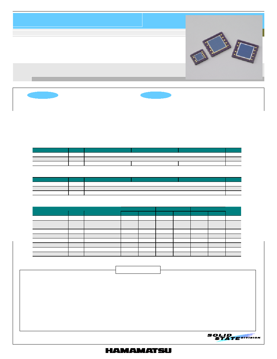
P H O T O D I O D E
Si PIN photodiode
Multi-element photodiodes for surface mounting
S5980, S5981, S5870
s
General ratings
Parameter
Symbol
S5980
S5981
S5870
Unit
Window material
-
Resin coating
-
Gap between elements
-
30
µm
Active area
A
F5.0/4 elements
F10.0/4 elements
F10.0/2 elements
mm
s
Absolute maximum ratings
Parameter
Symbol
S5980
S5981
S5870
Unit
Reverse voltage
V
R
Max.
30
V
Operating temperature
Topr
-40 to +100
∞C
Storage temperature
Tstg
-40 to +125
∞C
s
Electrical and optical characteristics (Ta=25 ∞C, per 1 element)
S5980
S5981
S5870
Parameter
Symbol
Condition
Typ.
Max.
Typ.
Max.
Typ.
Max.
Unit
Spectral response range
320 to 1100
-
320 to 1100
-
320 to 1100
-
nm
Peak sensitivity
wavelength
p
960
-
960
-
960
-
nm
Photo sensitivity
S
=p
0.72
-
0.72
-
0.72
-
A/W
Dark current
I
D
V
R
=10 V
0.3
2
0.6
4
2
10
nA
Temperature coefficient of I
D
T
CID
1.15
-
1.15
-
1.15
-
times/∞C
Cut-off frequency
fc
V
R
=10 V, R
L
=50 , -3 dB
25
-
20
-
10
-
MHz
Terminal capacitance
Ct
V
R
=10 V, f=1 MHz
10
-
35
-
50
-
pF
Noise equivalent power
NEP
1.4 ◊ 10
-14
-
1.9 ◊ 10
-14
-
3.5 ◊ 10
-14
-
W/Hz
1/2
Note) Package unit: S5980: 100 pieces, S5981, S5870: 70 pieces
q The light input window of this product uses soft silicone resin. Avoid touching the window to keep it from grime and damage that
can decrease sensitivity. External force applied to the resin surface may deform or cut off the wires, so do not touch the window
to prevent such troubles.
q Use rosin flux when soldering, to prevent the terminal lead corrosion. Reflow oven temperature should be at 260 ∞C maximum for 5
seconds maximum time under the conditions that no moisture absorption occurs.
Reflow soldering conditions differ depending on the type of PC board and reflow oven. Carefully check these conditions before use.
q Silicone resin swells when it absorbs organic solvent, so do not use any solvent other than alcohol.
q Avoid unpacking until you actually use this product to prevent the terminals from oxidation and dust deposits or the coated resin
from absorbing moisture.
When the product is stored for 3 months while not unpacked or 24 hours have elapsed after unpacking, perform baking in
nitrogen atmosphere at 150 ∞C for 3 to 5 hours or at 120 ∞C for 12 to 15 hours before use.
Precautions for use
HAMAMATSU PHOTONICS K.K., Solid State Division
1126-1 Ichino-cho, Hamamatsu City, 435-8558 Japan, Telephone: (81) 053-434-3311, Fax: (81) 053-434-5184, http://www.hamamatsu.com
U.S.A.: Hamamatsu Corporation: 360 Foothill Road, P.O.Box 6910, Bridgewater, N.J. 08807-0910, U.S.A., Telephone: (1) 908-231-0960, Fax: (1) 908-231-1218
Germany: Hamamatsu Photonics Deutschland GmbH: Arzbergerstr. 10, D-82211 Herrsching am Ammersee, Germany, Telephone: (49) 08152-3750, Fax: (49) 08152-2658
France: Hamamatsu Photonics France S.A.R.L.: 8, Rue du Saule Trapu, Parc du Moulin de Massy, 91882 Massy Cedex, France, Telephone: 33-(1) 69 53 71 00, Fax: 33-(1) 69 53 71 10
United Kingdom: Hamamatsu Photonics UK Limited: 2 Howard Court, 10 Tewin Road, Welwyn Garden City, Hertfordshire AL7 1BW, United Kingdom, Telephone: (44) 1707-294888, Fax: (44) 1707-325777
North Europe: Hamamatsu Photonics Norden AB: Smidesv‰gen 12, SE-171 41 Solna, Sweden, Telephone: (46) 8-509-031-00, Fax: (46) 8-509-031-01
Italy: Hamamatsu Photonics Italia S.R.L.: Strada della Moia, 1/E, 20020 Arese, (Milano), Italy, Telephone: (39) 02-935-81-733, Fax: (39) 02-935-81-741
Information furnished by HAMAMATSU is believed to be reliable. However, no responsibility is assumed for possible inaccuracies or omissions.
Specifications are subject to change without notice. No patent rights are granted to any of the circuits described herein. ©2001 Hamamatsu Photonics K.K.
Si PIN photodiode
S5980, S5981, S5870
Cat. No. KPIN1012E02
Apr. 2001 DN
0.03
0.03
10.0
a
b
d
c
ANODE b
NC
CATHODE COMMON
NC
ANODE c
ANODE d
NC
NC
NC
ANODE a
DETAILS OF
ACTIVE AREA
(4
◊) R0.3
16.5 ± 0.2
1.8
2.54
3.0
0.46
1.26 ± 0.15
(10
◊) 1.2
14.5 ± 0.2
1.8
Package burr may protrude a maximum of 0.3 mm
on each side from the outer edges.
ACTIVE AREA
PHOTOSENSITIVE
SURFACE
SILICONE
RESIN
0.03
10.0
a
b
NC
ANODE a
CATHODE COMMON
ANODE b
NC
NC
NC
NC
NC
NC
DETAILS OF
ACTIVE AREA
(4
◊) R0.3
16.5 ± 0.2
1.8
2.54
3.0
0.46
1.26 ± 0.15
(10
◊) 1.2
14.5 ± 0.2
1.8
Package burr may protrude a maximum of 0.3 mm
on each side from the outer edges.
ACTIVE AREA
PHOTOSENSITIVE
SURFACE
SILICONE
RESIN
8.8 ± 0.2
(4
◊) R0.3
10.6 ± 0.2
1.5
1.27
1.5
2.5
0.46
1.26 ± 0.15
0.03
0.03
5.0
a
b
d
c
(10
◊) 0.6
SILICONE
RESIN
Package burr may protrude a maximum of 0.3 mm
on each side from the outer edges.
ANODE b
NC
CATHODE COMMON
NC
ANODE c
ANODE d
NC
NC
NC
ANODE a
PHOTOSENSITIVE
SURFACE
DETAILS OF
ACTIVE AREA
ACTIVE AREA
0.6
0.5
0.4
0.3
0.1
200
400
600
800
1000
WAVELENGTH (nm)
PHOTO SENSITIVITY
(A/W)
0.7
0.8
(Typ. Ta=25 ∞C)
0.2
s
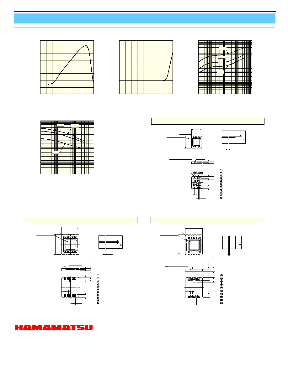
Spectral response
s
Dimensional outlines (unit: mm)
KMPDA0036EA
0
190
400
600
800
1000
+1.0
+0.5
(Typ. )
+1.5
-0.5
WAVELENGTH (nm)
TEMPERATURE COEFFICIENT
(%/
∞
C)
s
Photo sensitivity temperature characteristic
REVERSE VOLTAGE (V)
DARK CURRENT
100 pA
10 nA
1 nA
10 pA
1 pA
0.01
0.1
1
10
100
(Typ. Ta=25 ∞C)
S5980
S5981
S5870
s
Dark current vs. reverse voltage
REVERSE VOLTAGE (V)
TERMINAL CAPACITANCE
(Typ. Ta=25 ∞C, f=1 MHz)
1 nF
10 pF
1 pF
100 fF
0.1
1
10
100
100 pF
S5981
S5870
S5980
s
Terminal capacitance vs. reverse voltage
KMPDB0125EA
KMPDA0113EA
KMPDA0037EA
KMPDB0122EA
KMPDB0123EA
KMPDB0124EA
S5980
S5870
S5981