S5971, S5972, S5973 series
S5971, S5972 and S5973 series are high-speed Si PIN photodiodes designed for visible to near infrared light detection. These photodiodes
provide wideband characteristics at a low bias, making them suitable for optical communications and other high-speed photometry. S5973 series
includes a mini-lens type (S5973-01) that can be efficiently coupled to an optical fiber and a violet sensitivity enhanced type (S5973-02) ideal for
violet laser detection.
Features
l High-speed response
S5971 : 100 MHz (V
R
=10 V)
S5972 : 500 MHz (V
R
=10 V)
S5973 series: 1.5 GHz (V
R
=10 V)
l Low price
l High sensitivity
S5973-02: 0.3 A/W, QE=91 % (
=410 nm)
l High reliability
Applications
l Optical fiber communications
l High-speed photometry
l Violet laser detection (S5973-02)
P H O T O D I O D E
Si PIN photodiode
High-speed photodiodes (S5973 series: 1.5 GHz)
I General ratings / Absolute maximum ratings
Absolute maximum ratings
Package
Active area
size
Effective
active area
Reverse
voltage
V
4
Max.
Power
dissipation
P
Operating
temperature
Topr
Storage
temperature
Tstg
Type No.
Dimensional
outline/
Window
material *
1
(mm)
(mm)
(mm
2
)
(V)
(mW)
(∞C)
(∞C)
S5971
f1.2
1.1
S5972
f0.8
0.5
S5973
/K
S5973-01
/L
S5973-02
/K
TO-18
f0.4
0.12
20
50
-40 to +100 -55 to +125
I Electrical and optical characteristics
Photo sensitivity
S
(A/W)
Spectral
response
range
l
Peak
sensitivity
wavelength
lp
Short
circuit
current
Isc
100 lx
Dark
current
I
,
V
4
=10 V
(nA)
Temp.
coefficient
of
I
,
T
+1,
Cut-off
frequency
fc
V
4
=10 V
Terminal
capacitance
Ct
V
4
=10 V
f=1 MHz
NEP
V
4
=10 V
Type No.
(nm)
(nm)
lp
660
nm
780
nm
830
nm
(µA)
Typ. Max. (times/∞C) (GHz)
(pF)
(W/Hz
1/2
)
S5971
320 to
1060
900
0.64
0.6
1.0
0.07
1
0.1
7.4 ◊ 10
-15
S5972
800
0.57
0.55
0.55 0.42
0.01
0.5
0.5
3
3.1 ◊ 10
-15
S5973
0.09
S5973-01
0.52
0.44
0.51 0.47
0.42
1.5
S5973-02
320 to
1000
760
0.45 0.3 *
2
0.42 0.37 0.06
0.002 0.1
1.15
1.5
1.6
1.5 ◊ 10
-15
*1: Window material K: borosilicate glass, L: lens type borosilicate glass
*2: l=410 nm
1

Si PIN photodiode
S5971, S5972, S5973 series
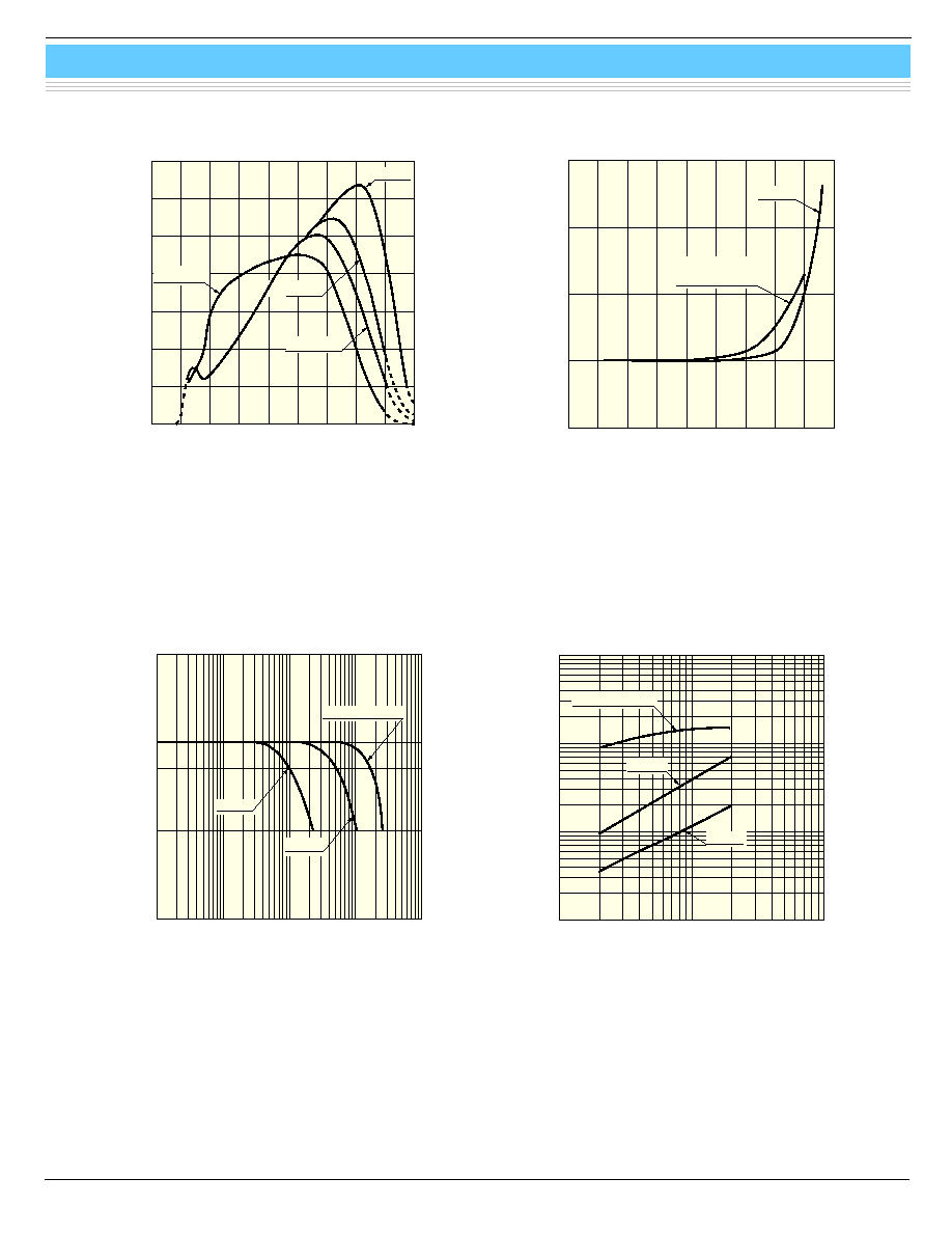
FIBER-COUPLED SENSITIVITY (A/W)
SHIFT FROM LENS CENTER X, Y (mm)
(Typ. Ta=25 ∞C,
=780 nm, NA=0.2)
Z
Y
X
0.6
0.5
0.4
0.3
0.2
0.1
0
-0.8
-0.4
0
+0.4
+0.8
OPTICAL FIBER
(CORE DIAMETER: 50 µm)
LIGHT SOURCE=780 nm LD
Z=0.5 mm
100 fA
1 pA
10 pA
100 pA
0.1
1
REVERSE VOLTAGE (V)
DARK CURRENT
(Typ. Ta=25 ∞C)
10
100
S5971
S5972
S5973 SERIES
I Dark current vs. reverse voltage
I Terminal capacitance vs. reverse voltage
KPINB0161EA
1 pF
10 pF
100 pF
0.1
1
REVERSE VOLTAGE (V)
TERMINAL CAPACITANCE
(Typ. Ta=25 ∞C, f=1 MHz)
10
100
S5971
S5972
S5973 SERIES
KPINB0162EA
I Fiber coupling characteristics (S5973-01)
X, Y direction
Z direction
0.6
0.5
0.4
0.3
0.2
0.1
0
0.2
0.5
1
2
5
10
20
Z
Y
X
OPTICAL FIBER
(CORE DIAMETER: 50 µm)
LIGHT SOURCE =780 nm LD
X, Y= 0 mm
FIBER-COUPLED SENSITIVITY (A/W)
DISTANCE BETWEEN LENS AND FIBER END Z (mm)
(Typ. Ta=25 ∞C,
=780 nm, NA=0.2)
KPINB0088EA
KPINB0089EA
3
Si PIN photodiode
S5971, S5972, S5973 series
HAMAMATSU PHOTONICS K.K., Solid State Division
1126-1 Ichino-cho, Hamamatsu City, 435-8558 Japan, Telephone: (81) 053-434-3311, Fax: (81) 053-434-5184, http://www.hamamatsu.com
U.S.A.: Hamamatsu Corporation: 360 Foothill Road, P.O.Box 6910, Bridgewater, N.J. 08807-0910, U.S.A., Telephone: (1) 908-231-0960, Fax: (1) 908-231-1218
Germany: Hamamatsu Photonics Deutschland GmbH: Arzbergerstr. 10, D-82211 Herrsching am Ammersee, Germany, Telephone: (49) 08152-3750, Fax: (49) 08152-2658
France: Hamamatsu Photonics France S.A.R.L.: 8, Rue du Saule Trapu, Parc du Moulin de Massy, 91882 Massy Cedex, France, Telephone: 33-(1) 69 53 71 00, Fax: 33-(1) 69 53 71 10
United Kingdom: Hamamatsu Photonics UK Limited: 2 Howard Court, 10 Tewin Road, Welwyn Garden City, Hertfordshire AL7 1BW, United Kingdom, Telephone: (44) 1707-294888, Fax: (44) 1707-325777
North Europe: Hamamatsu Photonics Norden AB: Smidesv‰gen 12, SE-171 41 Solna, Sweden, Telephone: (46) 8-509-031-00, Fax: (46) 8-509-031-01
Italy: Hamamatsu Photonics Italia S.R.L.: Strada della Moia, 1/E, 20020 Arese, (Milano), Italy, Telephone: (39) 02-935-81-733, Fax: (39) 02-935-81-741
Information furnished by HAMAMATSU is believed to be reliable. However, no responsibility is assumed for possible inaccuracies or omissions.
Specifications are subject to change without notice. No patent rights are granted to any of the circuits described herein. ©2003 Hamamatsu Photonics K.K.
Cat. No. KPIN1025E03
Mar. 2003 DN
13
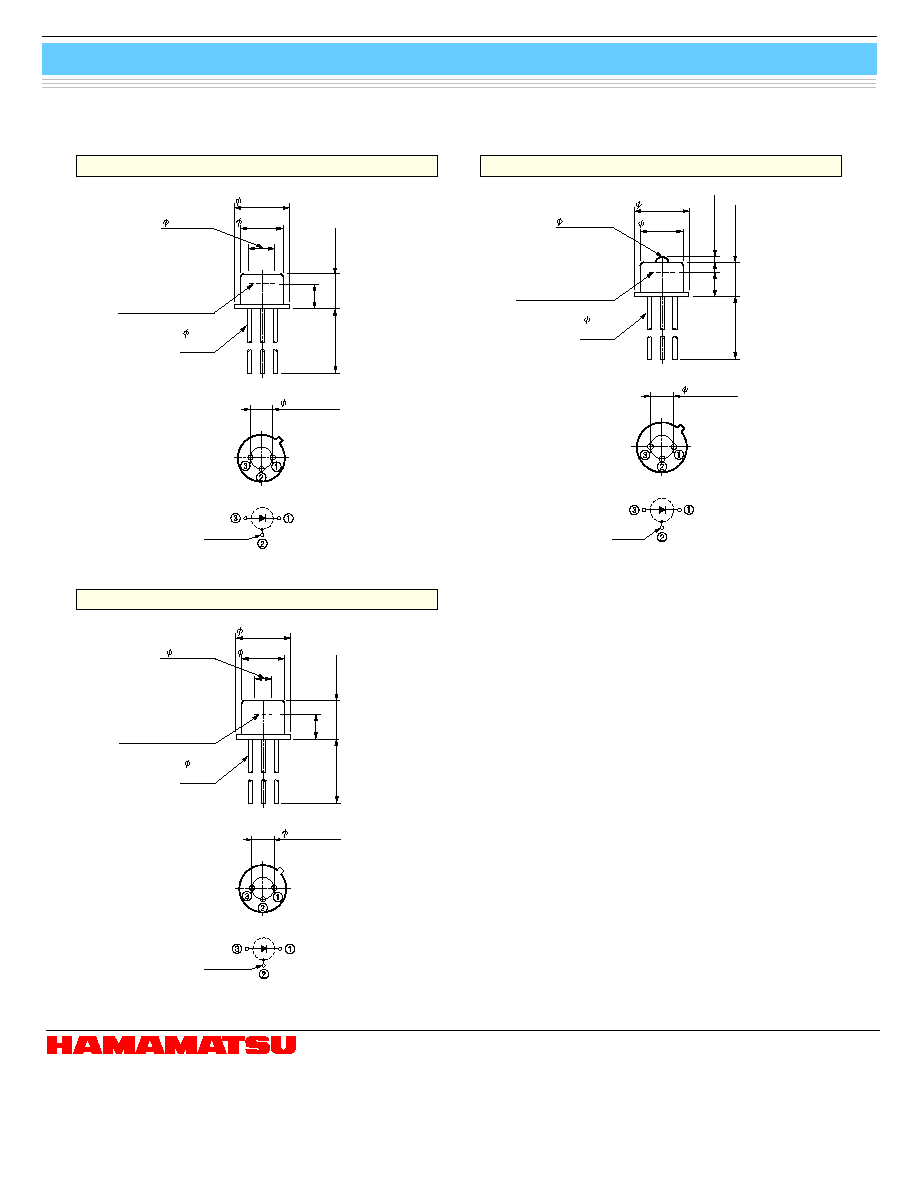
2.8
3.6 ± 0.2
0.45
LEAD
4.7 ± 0.1
5.4 ± 0.2
2.54 ± 0.2
CASE
PHOTOSENSITIVE
SURFACE
WINDOW
3.0 ± 0.2
KPINA0022EB
13.5
0.65 ± 0.15
3.75 ± 0.2
0.45
LEAD
4.6 ± 0.1
5.4 ± 0.2
PHOTOSENSITIVE
SURFACE
2.8
2.54 ± 0.2
CASE
WINDOW
1.5 LENS
KPINA0023EA
KPINA0061EA
S5973-02
13
2.8
4.0 ± 0.2
0.45
LEAD
4.6 ± 0.1
5.4 ± 0.2
2.54 ± 0.2
CASE
PHOTOSENSITIVE
SURFACE
WINDOW
2.0 MIN.
I Dimensional outlines (unit: mm)
S5971, S5972, S5973 S5973-01
4