S6431, S6432, S7481, S7482
S6431, S6432, S7481 and S7482 are high-speed APC detectors developed for monitoring laser diodes with a peak wavelength shorter than 700
nm. All types are designed for surface mount, and S6431 and S6432 have the terminals for positioning easily.
Features
l High-speed response at low reverse voltage
S6431, S7481 (
0.8 mm) : 500 MHz Typ. (V
R
=2.5 V)
S6432, S7482 (
0.6 mm) : 600 MHz Typ. (V
R
=2.5 V)
l S6431, S6432: Clear plastic package with wire
connection terminals (4 ◊ 4.8 mm)
l High sensitivity: 0.48 A/W Typ. (=660 nm)
Applications
l Laser diode monitor of optical disk unit (high-speed APC)
l Sensor for red laser diode
P H O T O D I O D E
Si PIN photodiode
High-speed detector with surface-mount plastic package
s
General ratings / Absolute maximum ratings
Absolute maximum ratings
Active area
size
Effective active
area
Reverse
voltage
V
R
Max.
Power
dissipation
P
Operating
temperature
Topr
Storage
temperature
Tstg
Type No.
Dimensional
outline
Package
(mm)
(mm
2
)
(V)
(mV)
(∞C)
(∞C)
S6431
0.8
0.5
S6432
0.6
0.28
S7481
0.8
0.5
S7482
Plastic
0.6
0.28
20
50
-25 to +85 -40 to +100
s
Electrical and optical characteristics
Photo sensitivity
S
(A/W)
Spectral
response
range
Peak
sensitivity
wavelength
p
Short
circuit
current
Isc
100 lx
Dark
current
I
D
V
R
=2.5 V
Temp.
coefficient
of
I
D
T
CID
Cut-off
frequency
fc
V
R
=2.5 V
R
L
=50
Terminal
capacitance
Ct
V
R
=2.5 V
f=1 MHz
NEP
V
R
=2.5 V
Type No.
(nm)
(nm)
p
660
nm
780
nm
830
nm
(µA)
Typ.
(nA)
Max.
(nA) (times/∞C)
Min.
(MHz)
Typ.
(MHz)
Typ.
(pF)
Max.
(pF) (W/Hz
1/2
)
S6431
0.48
300 500
6
12
S6432
0.25
400 600
3
6
S7481
0.48
300 500
6
12
S7482
320 to
1000
760
0.5 0.48 0.5 0.45
0.25
0.01 0.3
1.15
400 600
3
6
3.6 ◊ 10
-15
*1: =680 nm
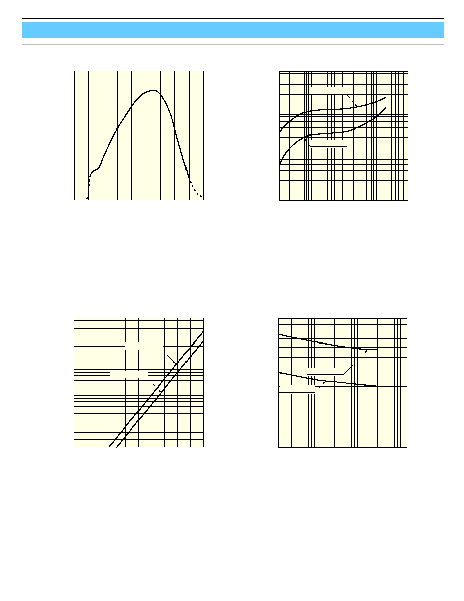
Si PIN photodiode
S6431, S6432, S7481, S7482
0
0.1
0.2
0.3
0.4
200
400
600
800
1000
WAVELENGTH (nm)
PHOTO SENSITIVITY
(A/W)
(Typ. Ta=25 ∞C)
0.5
0.6
s
Spectral response
KPINB0171EA
10 fA
100 fA
1 pA
10 pA
0.01
0.1
1
10
100
REVERSE VOLTAGE (V)
DARK CURRENT
(Typ. Ta=25 ∞C)
S6431, S7481
S6432, S7482
KPINB0172EA
1 pA
10 pA
100 pA
1 nA
10 nA
100 fA
-20
0
20
40
60
AMBIENT TEMPERATURE (∞C)
DARK CURRENT
80
(Typ. V
R
=2.5 V)
S6431, S7481
S6432, S7482
s
Dark current temperature characteristics
KPINB0173EA
1 pF
10 pF
0.1
1
10
100
REVERSE VOLTAGE (V)
TERMINAL CAPACITANCE
(Typ. Ta=25 ∞C, f=1 MHz)
S6431, S7481
S6432, S7482
KPINB0174EA
s
Terminal capacitance vs. reverse voltage
s
Dark current vs. reverse voltage
Si PIN photodiode
S6431, S6432, S7481, S7482
HAMAMATSU PHOTONICS K.K., Solid State Division
1126-1 Ichino-cho, Hamamatsu City, 435-8558 Japan, Telephone: (81) 053-434-3311, Fax: (81) 053-434-5184, http://www.hamamatsu.com
U.S.A.: Hamamatsu Corporation: 360 Foothill Road, P.O.Box 6910, Bridgewater, N.J. 08807-0910, U.S.A., Telephone: (1) 908-231-0960, Fax: (1) 908-231-1218
Germany: Hamamatsu Photonics Deutschland GmbH: Arzbergerstr. 10, D-82211 Herrsching am Ammersee, Germany, Telephone: (49) 08152-3750, Fax: (49) 08152-2658
France: Hamamatsu Photonics France S.A.R.L.: 8, Rue du Saule Trapu, Parc du Moulin de Massy, 91882 Massy Cedex, France, Telephone: 33-(1) 69 53 71 00, Fax: 33-(1) 69 53 71 10
United Kingdom: Hamamatsu Photonics UK Limited: 2 Howard Court, 10 Tewin Road, Welwyn Garden City, Hertfordshire AL7 1BW, United Kingdom, Telephone: (44) 1707-294888, Fax: (44) 1707-325777
North Europe: Hamamatsu Photonics Norden AB: Smidesv‰gen 12, SE-171 41 Solna, Sweden, Telephone: (46) 8-509-031-00, Fax: (46) 8-509-031-01
Italy: Hamamatsu Photonics Italia S.R.L.: Strada della Moia, 1/E, 20020 Arese, (Milano), Italy, Telephone: (39) 02-935-81-733, Fax: (39) 02-935-81-741
Information furnished by HAMAMATSU is believed to be reliable. However, no responsibility is assumed for possible inaccuracies or omissions.
Specifications are subject to change without notice. No patent rights are granted to any of the circuits described herein. ©2001 Hamamatsu Photonics K.K.
Cat. No. KPIN1018E02
Apr. 2001 DN
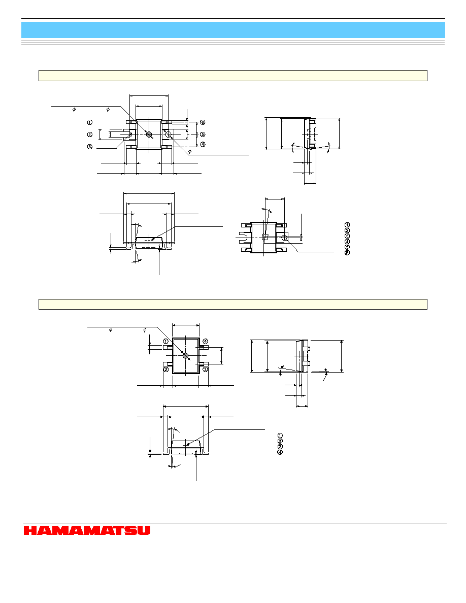
KPINA0038EA
7.0 ± 0.3
0.7 ± 0.3
0.7 ± 0.3
0.25
0.1 ± 0.1
5∞
10∞
7.9 ± 0.3
X=3.0 ± 0.1
Y
±0.1
(BASIC HOLE)
±2∞
4.1 ± 0.2
(INCLUDING BURR)
6.0 ± 0.06
1.77
1.95 ± 0.4
1.5 ± 0.4
1.5 ± 0.4
1.95 ± 0.4
4.0
1.77
0.5
1.905
1.905
0.9
-0
(BASIC HOLE)
+0.06
ACTIVE AREA
(S6431: 0.8, S6432: 0.6)
R0.4
-0
4.7
5.0 ± 0.2
(INCLUDING BURR)
1.8
0.8
10
∞
0.4
Chip position accuracy faces
center of basic hole
5
∞
4.8
0.8
-0
+0.03
+0.06
PHOTOSENSITIVE
SURFACE
NC
CATHODE (COMMON)
NC
ANODE
CATHODE (COMMON)
CATHODE (COMMON)
Tolerance unless otherwise
noted: ±0.1
5.0 ± 0.2
(INCLUDING BURR)
4.7 *
10
∞
4.8 *
5
∞
0.4
0.6
2.54
1.5 ± 0.4
1.5 ± 0.4
1.8
0.8
10∞
5∞
7.0 ± 0.3
0.7 ± 0.3
0.7 ± 0.3
0.25
0.1 ± 0.1
PHOTOSENSITIVE
SURFACE
4.0 *
4.1 ± 0.2
(INCLUDING BURR)
ACTIVE AREA
(S7481: 0.8, S7482: 0.6)
NC
CATHODE
ANODE
CATHODE
Chip position accuracy with respect to the
package dimensions marked *
X, Y
±0.2
Q
±2∞
Tolerance unless otherwise
noted: ±0.1
KPINA0053EA
s
s
s
s
s
Dimensional outline (unit: mm)
S6431, S6432
S7481, S7482