 | –≠–ª–µ–∫—Ç—Ä–æ–Ω–Ω—ã–π –∫–æ–º–ø–æ–Ω–µ–Ω—Ç: S6493-64 | –°–∫–∞—á–∞—Ç—å:  PDF PDF  ZIP ZIP |
S6493/S6494 series
S6493 and S6494 series are Si photodiode arrays efficiently combined with a signal processing circuit. The signal processing circuit is formed on
a single chip by the CMOS process, and includes a shift register, clamp circuit, hold circuit and charge amplifier array, thus allowing a simplified
external circuit configuration.
The photocurrent from the photodiode array is fed to the charge amplifier connected to each element and is converted into a voltage.
The signal voltage is then sent to the clamp circuit and hold circuit, and is finally read out from the shift register in turn as a sequential video
signal. The signal readout is performed by means of the charge storage method, so the output is proportional to the amount of light exposure (the
product of incident light level and integration time). The vide output is a boxcar waveform which is low noise and easy to handle.
In addition, the readout gain can be selected from two levels by changing the voltage to the external input terminal. (The "high" gain is 10 times
that of the "low" gain.) S6493 and S6494 series ensure easy operation since they can operate from a 5 V supply, and yet offer a maximum data
rate of 250 kHz.
Features
l Four types are available
S6493-64: 0.8 mm pitch ◊ 64 ch
S6493-128: 0.4 mm pitch ◊ 128 ch
S6494-64: 1.6 mm pitch ◊ 64 ch
S6494-128: 0.8 mm pitch ◊ 128 ch
l Simultaneous integration by using a charge amplifier array
l Sequential readout with a shift register
l Integrated clamp circuit allows low noise and wide
dynamic range
l Two gain levels can be selected
l Operates from single 5 V supply input
l S6493 series:
Long active area can be configured by use of multiple arrays
phosphor screen type is also available for X-ray detection
l Custom designed element size and pitch available
l Dedicated driver circuits are available
Applications
l Image or pattern recognition system
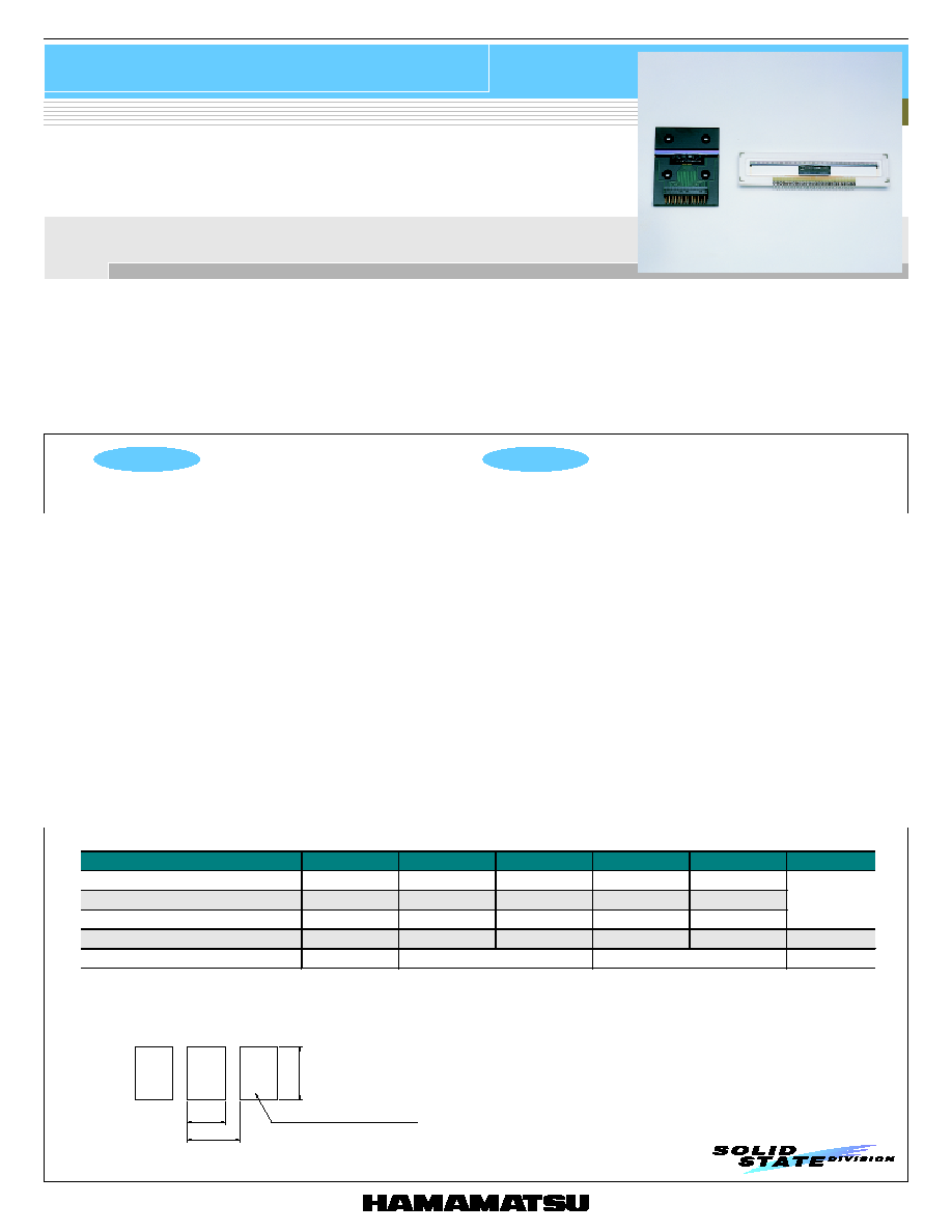
P H O T O D I O D E
Photodiode array with amplifier
Photodiode arrays combined with a signal processing circuit chip
s Detail of elements
KMPDC0072EA
H
W
P
PHOTODIODE DIFFUSION AREA
s Mechanical specifications
Parameter
Symbol *
1
S6493-64
S6493-128
S6494-64
S6494-128
Unit
Element pitch
P
0.8
0.4
1.6
0.8
Element diffusion width
W
0.6
0.25
1.3
0.6
Element height
H
0.8
0.4
1.6
0.8
mm
Number of elements
-
64
128
64
128
-
Active area length
-
51.2
102.4
mm
*1: Refer to following figure
1
Photodiode array with amplifier
S6493/S6494 series
s Absolute maximum ratings
Parameter
Symbol
Value
Unit
Supply voltage
Vdd
Gain selection terminal voltage
Vgain
Clock pulse voltage
V
1, V2
Start pulse voltage
V
st
Reset pulse voltage
V
reset
Hold pulse voltage
V
hold
Sample pulse voltage
V
sample
Clamp pulse voltage
V
clamp
-0.3 to +7.0
V
Operating temperature
*
2
Topr
-5 to +60
Storage temperature
Tstg
-10 to +70
∞C
*2: No condensation
s Recommended terminal voltage
Parameter
Symbol
Min.
Typ.
Max.
Unit
Supply voltage
Vdd
4.8
5
5.2
Low gain
Vgain (L)
Vdd-0.2
Vdd
Vdd+0.2
Gain selection
terminal voltage
High gain
Vgain (H)
0
-
0.4
High level
Vdd-0.2
Vdd
Vdd+0.2
Clock pulse voltage
Low level
V
1, V2
0
-
0.4
High level
Vdd-0.2
Vdd
Vdd+0.2
Start pulse voltage
Low level
V
st
0
-
0.4
High level
Vdd-0.2
Vdd
Vdd+0.2
Reset pulse voltage
Low level
V
reset
0
-
0.4
High level
Vdd-0.2
Vdd
Vdd+0.2
Hold pulse voltage
Low level
V
hold
0
-
0.4
High level
Vdd-0.2
Vdd
Vdd+0.2
Sample pulse voltage
Low level
V
sample
0
-
0.4
High level
Vdd-0.2
Vdd
Vdd+0.2
Clamp pulse voltage
Low level
V
clamp
0
-
0.4
V
s Electrical characteristics (Ta=25 ∞C, Vdd=5 V, V
1=V2=Vreset=Vhold=Vclamp=Vsample=5 V)
S6493-64, S6494-64
S6493-128, S6494-128
Parameter
Symbol
Min.
Typ.
Max.
Min.
Typ.
Max.
Unit
Clock pulse frequency (video data rate)
f
1, f2
15
-
250
15
-
250
kHz
Integration time
Ts
0.3
-
10
0.6
-
10
ms
Clock pulse line capacitance
C
1, C2
-
15
-
-
30
-
Video line capacitance
Cv
-
20
-
-
40
-
pF
Output impedance
Zo
-
3
-
-
3
-
k
Current consumption
Idd
-
20
-
-
40
-
mA
2

Photodiode array with amplifier
S6493/S6494 series
s Electrical and optical characteristics
S6493-64
S6493-128
S6494-64
S6494-128
Parameter
Symbol
Min.
Typ. Max. Min.
Typ. Max. Min.
Typ. Max. Min.
Typ. Max.
Unit
Spectral response range
200 to 1000
200 to 1000
320 to 1000
320 to 1000
Peak sensitivity wavelength
p
-
720
-
-
720
-
-
720
-
-
720
-
nm
High gain
-
0.4
4
-
0.2
2
-
0.8
8
-
0.4
4
Dark output
voltage *
3
Low gain
Vd
-
0.04
0.4
-
0.02
0.2
-
0.08
0.8
-
0.04
0.4
mV
Saturation output voltage *
3
Vsat
1.3
1.6
-
1.3
1.6
-
1.3
1.6
-
1.3
1.6
-
V
High gain
-
1.2
-
-
5.8
-
-
0.28
-
-
1.2
-
Saturation
exposure *
4, 5
Low gain
Esat
-
12
-
-
58
-
-
2.8
-
-
12
-
mlx∑s
High gain
-
1300
-
-
270
-
-
5700
-
-
1300
-
Photo sensitivity *
5
Low gain
S
-
130
-
-
27
-
-
570
-
-
130
-
V/lx∑s
Photo response non-uniformity *
6
PRNU
-
-
20
-
-
20
-
-
20
-
-
20
%
High gain
-
0.2
-
-
0.2
-
-
0.3
-
-
0.3
-
Noise *
7
Low gain
N
-
0.2
-
-
0.2
-
-
0.2
-
-
0.2
-
mVrms
Output offset voltage *
8
Vos
2.5
3
3.5
2.5
3
3.5
2.5
3
3.5
2.5
3
3.5
V
[Ta=25 ∞C, Vdd=5 V, V
1=V2=Vreset =Vhold =Vclamp =Vsample=5 V, Vgain=5 V (Low gain), 0 V (High gain),
Data rate: 200 kHz]
*3: Integration time ts=1 ms
*4: Saturation output voltage and exposure are determined by the upper limit of the charge amplifier.
*5: Measured with a 2856 K tungsten lamp.
*6: When the photodiode array is exposed to uniform light which is 50 % of the saturation exposure, the Photo Response Non-
Uniformity (PRNU) is defined as follows:
PRNU = (Vmax - Vmin)/Vaverage ◊ 100 (%)
where Vaverage is the average output of all elements, Vmax is the output of the element that provides the maximum output,
Vmin is the output of the element that provides the minimum output.
*7: Measured at a data rate of 50 kHz and integration time of 5 ms under dark condition.
*8: The output offset voltage is defined as shown in following figure (Output waveform of one element).
s Output waveform of one element
s Spectral response
KMPDB0041EA
s Driver circuit consideration
The following points must be taken into account when you use a driver circuit.
q The input pulse must meet the pulse conditions at the input terminal. Each pulse should be amplified by the buffer at a
position as close to the input terminal as possible.
q The video output should undergo non-inverting amplification at the external readout circuit.
q Use of a JFET input type op amp is recommended. Make offset adjustment as necessary. In this case, it should be
noted that the dark output level appears on the lower voltage side relative to the output offset voltage.
0.1
PHOTO SENSITIVITY (A/W)
190
400
600
800
1000
WAVELENGTH (nm)
0.3
0.2
(Typ. Ta =25 ∞C)
0.4
S6493 SERIES
S6494 SERIES
0
KMPDC0077EA
DARK STATE
120 mV Typ.
GND
OFFSET VOLTAGE
V
OS
=3 V Typ.
SATURATION OUTPUT
VOLTAGE
Vsat=1.6 V Typ.
SATURATION STATE
3

Photodiode array with amplifier
S6493/S6494 series
s Block diagram
q Charge integration operation
(1) When a
reset pulse is input, all elements in the integration amplifier are reset to start integration.
(2) When a
hold pulse is input, output from all elements of the integration amplifier is simultaneously sent to the output hold
circuit.
(3) The charge integration time is equal to the time interval from the
reset pulse input to the hold input.
(4) When another
reset pulse is input, the next integration starts.
(5) The
clamp and sample pulses are needed to operate the clamp circuit.
q Readout operation
(1) Under the condition that complimentary clock pulse
1 and 2 are being supplied, the shift register starts operation when a st
pulse is loaded. At this point, the
1 pulse must rise only once while the st is low.
(2) The shift register generates an address pulse train, and the output signal accumulated in the hold circuit is read out in t
urn
from the first element, as a sequential signal from the Video terminal.
(3) The video signal is obtained as a boxcar waveform in synchronization with the positive-going edge of
2.
(4) The
hold pulse cannot be loaded during readout operation (shift register operation).
(5) The EOS (end-of-scan) signal is output in synchronization with the negative-going edge of
1 immediately before the output
timing of the last element.
q Serial readout for multistage arrangement (S6493 series)
When multiple photodiode arrays are used in a serial arrangement, charge integration of each board can be performed at the same
time, but the shift register of each board should be operated in sequence. The EOS pulse can be used as a start pulse for the n
ext stage
when it is inverted.
The video output terminal from all boards shoud be combined as one line via an analog switch and then connected to the external
readout circuit. The analog switch should be used to select the video output only of the board being read out.
s Recommended timing chart
The operations of the S6493 and S6494 series devices can be divided into charge integration and readout operations, as follows:
KMPDC0073EA
KMPDC0078EA
1
2
3
4
N-3 N-2 N-1 N
Vdd Vss
Video
EOS
SHIFT RESISTER
HOLD CIRCUIT
CLAMP CIRCUIT
CHARGE AMPLIFIER
PHOTODIODE
st
1
2
hold
clamp
sample
reset
Vgain
st
INTEGRATION TIME
15 µs MIN.
1 µs MIN.
1
2
reset
hold
sample
clamp
Video
EOS
1
2
3
4
5
1
2
3
n-2 n-1 n
4

Photodiode array with amplifier
S6493/S6494 series
s Timing chart
Parameter
Symbol
Min.
Typ.
Max.
Unit
Start pulse width
tpw (
st)
300
-
-
Rise/fall time of start pulse
tr (
st), tf (st)
0
20
100
Clock pulse (
1, 2) width
tpw (
1, 2)
200
-
-
Rise/fall time of clock pulse (
1, 2)
tr (
1, 2), tf (1, 2)
0
20
100
ns
Hold pulse width
tpw (
h)
1
-
-
µs
Rise/fall time of hold pulse
tr (
h), tf (h)
0
20
100
ns
Reset pulse width
tpw (
r)
15
-
-
µs
Rise/fall time of reset pulse
tr (
r), tf (r)
0
20
100
Sample pulse (1) width
tpw (
s1)
500
-
-
Rise/fall time of sample pulse (1)
tr (
s1), tf (s1)
0
20
100
ns
Sample pulse (2) width
tpw (
s2)
tpw (
r)
-
-
µs
Rise/fall time of sample pulse (2)
tr (
s2), tf (s2)
0
20
100
ns
Clamp pulse width
tpw (
c)
tpw (
r)
-
-
µs
Rise/fall time of clamp pulse
tr (
c), tf (c)
0
20
100
Sample pulse (1) - hold pulse timing
t (
s1-h)
0
-
-
Hold pulse - reset pulse timing
t (
h-r)
0
-
-
Reset pulse - clamp pulse timing
t (
r-c)
0
-
-
Start pulse - clock pulse (
1, 2) timing 1
t1 (
st-1)
0
-
-
Start pulse - clock pulse (
1, 2) timing 2
t2 (
st-1)
0
-
-
Clock pulse (
1, 2) - start pulse timing 1
t1 (
1-st)
0
-
-
Clock pulse (
1, 2) - start pulse timing 2
t2 (
1-st)
0
-
-
ns
Video delay time
tvd
-
1
-
µs
EOS pulse delay time
ted
-
100
-
ns
KMPDC0079EA
tf ( r)
tf ( st)
tr ( st)
tpw ( st)
t1 ( 1- st)
tf ( 1)
tr ( 2)
tr ( 1)
tf ( 2)
tpw ( 1)
tpw ( 2)
t2 ( 1- st)
t1 ( st- 1)
t2 ( st- 1)
t ( h- r)
tpw ( h)
tr ( h)
reset
1
1
2
1
EOS
90 %
tvd
ted
Video
st
hold
sample
clamp
tr ( r)
t ( r- c)
tf ( s2)
tr ( s2)
tr ( s1)
tpw ( s1)
tr ( c)
tf ( c)
tpw ( c)
tf ( s1)
tpw ( r)
tf ( h)
5