P H O T O D I O D E
Si photodiode
High reliability photodiode
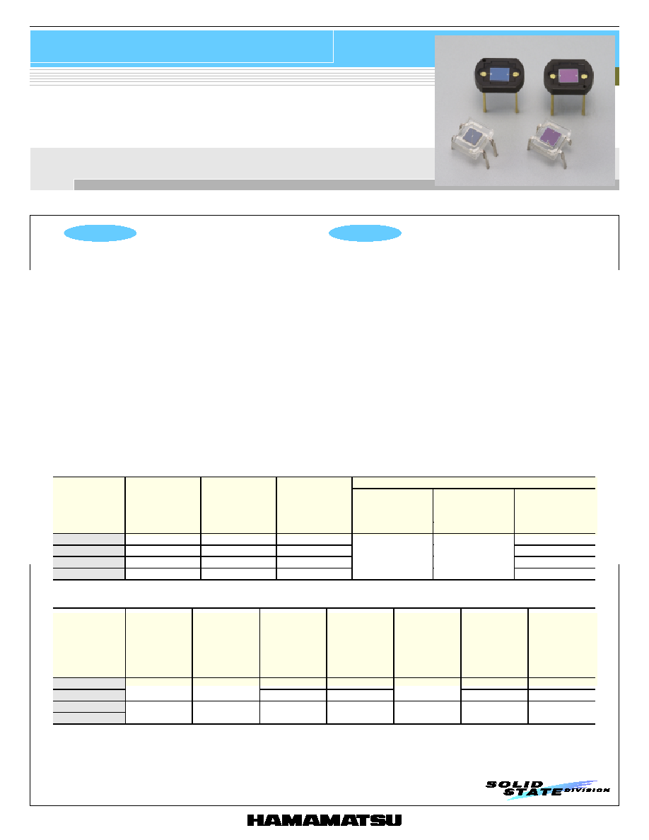
S6865/S7123 series
Features
l Two package types provided
S6865-01, S7123-01: plastic package
S6865-02, S7123-02: ceramic package
l Choice of two spectral response characteristics
S6865 series: visible to infrared range (320 to 1100 nm)
S7123 series: visible range (320 to 840 nm)
Applications
l Automobile sensors (for auto light control, display light dimmer)
l Copiers
l Cameras
l Other visible light sensors
S6865/S7123 series operate with high reliability over a wide temperature range (-40 to +100 ∞C). S6865 series has spectral response from
the visible to infrared range, while S7123 series has spectral response in the visible range.
s
General ratings / Absolute maximum ratings
Absolute maximum ratings
Active
area size
Effective
active area
Reverse voltage
V
R
Max.
Operating
temperature
Topr
Storage
temperature
Tstg
Type No.
Dimensional
outline
(mm)
(mm
2
)
(V)
(∞C)
(∞C)
S6865-01
2 ◊ 2
4
-40 to +125
S6865-02
2.4 ◊ 2.8
6.7
-55 to +125
S7123-01
2.46 ◊ 2.46
6.0
-40 to +125
S7123-02
2.4 ◊ 2.8
6.7
10
-40 to +100
-55 to +125
s
Electrical and optical characteristics (Typ. Ta=25 ∞C, unless otherwise noted)
Spectral
response
range
Peak
sensitivity
wavelength
p
Photo
sensitivity
S
=p
Short circuit
current
Isc
100 lx
2856 K
Dark current
I
D
V
R
=1 V
Max.
Rise time
tr
V
R
=0 V
R
L
=1 k
Terminal
capacitance
Ct
V
R
=0 V
f=10 kHz
Type No.
(nm)
(nm)
(A/W)
(µA)
(pA)
(µs)
(nF)
S6865-01
0.58
4
2
0.5
S6865-02
320 to 1100
960
0.7
6.5
10
2.5
0.7
S7123-01
S7123-02
320 to 840
540
0.3
0.9
100
10
3
Si photodiode
S6865/S7123 series
HAMAMATSU PHOTONICS K.K., Solid State Division
1126-1 Ichino-cho, Hamamatsu City, 435-8558 Japan, Telephone: (81) 053-434-3311, Fax: (81) 053-434-5184, http://www.hamamatsu.com
U.S.A.: Hamamatsu Corporation: 360 Foothill Road, P.O.Box 6910, Bridgewater, N.J. 08807-0910, U.S.A., Telephone: (1) 908-231-0960, Fax: (1) 908-231-1218
Germany: Hamamatsu Photonics Deutschland GmbH: Arzbergerstr. 10, D-82211 Herrsching am Ammersee, Germany, Telephone: (49) 08152-3750, Fax: (49) 08152-2658
France: Hamamatsu Photonics France S.A.R.L.: 8, Rue du Saule Trapu, Parc du Moulin de Massy, 91882 Massy Cedex, France, Telephone: 33-(1) 69 53 71 00, Fax: 33-(1) 69 53 71 10
United Kingdom: Hamamatsu Photonics UK Limited: 2 Howard Court, 10 Tewin Road, Welwyn Garden City, Hertfordshire AL7 1BW, United Kingdom, Telephone: (44) 1707-294888, Fax: (44) 1707-325777
North Europe: Hamamatsu Photonics Norden AB: Smidesv‰gen 12, SE-171 41 Solna, Sweden, Telephone: (46) 8-509-031-00, Fax: (46) 8-509-031-01
Italy: Hamamatsu Photonics Italia S.R.L.: Strada della Moia, 1/E, 20020 Arese, (Milano), Italy, Telephone: (39) 02-935-81-733, Fax: (39) 02-935-81-741
Information furnished by HAMAMATSU is believed to be reliable. However, no responsibility is assumed for possible inaccuracies or omissions.
Specifications are subject to change without notice. No patent rights are granted to any of the circuits described herein. ©2001 Hamamatsu Photonics K.K.
Cat. No. KSPD1024
E01
Apr. 2001 DN
4.6 ± 0.2
(INCLUDING BURR)
4.5 *
5.75 ± 0.2
0.25
5∞
7.5 ± 5∞
4.5 ± 0.4
5.4 *
10
∞
5.5 *
2.54
0.5
0.7
3
∞
2.0
1.0
0.7
3∞
ANODE
CATHODE
ANODE
CATHODE
Tolerance unless
otherwise noted: ±0.1
Chip position accuracy
with respect to the package
dimensions marked *
X, Y
±0.2
±2∞
5.6 ± 0.2
(INCLUDING BURR)
PHOTOSENSITIVE
SURFACE
ACTIVE AREA
2 ◊ 2
s
Dimensional outline (unit: mm)
KSPDA0124EA
0
200
400
600
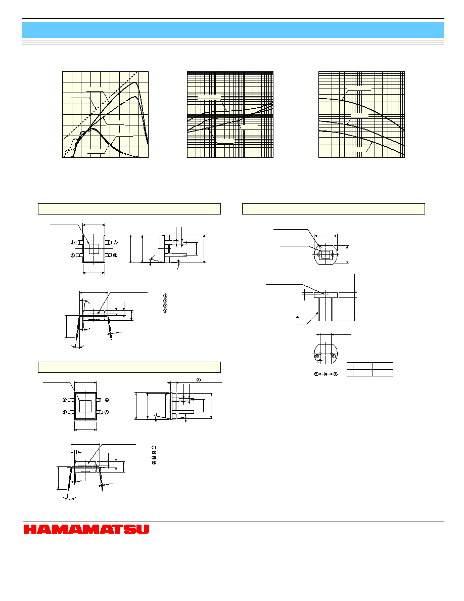
WAVELENGTH (nm)
PHO
T
O
SENSITIVITY (A/W)
800
1000
(Typ. Ta=25 ∞C)
0.1
0.2
0.3
0.4
0.5
0.6
0.7
0.8
QE=100 %
S7123-02
S6865-01
S7123-01
S6865-02
s
Spectral response
KSPDB0134EB
s
Dark current vs. reverse voltage
s
Terminal capacitance vs. reverse voltage
S6865-01
8.0
CATHODE
TERMINAL MARK
6.0
a
9 ± 1
1.5 ± 0.2
5.0 ± 0.2
+
0.1
-
0.3
+0
-0.25
a
S6865-02
0.7
S7123-02
0.6
ACTIVE AREA
2.4 ◊ 2.8
PHOTOSENSITIVE
SURFACE
Tolerance unless
otherwise noted: ±0.15
0.45
LEAD
S6865-02, S7123-02
KSPDA0125EA
4.6 ± 0.2
(INCLUDING BURR)
4.5 *
5.6 ± 0.2
(INCLUDING BURR)
5.4 *
10
∞
3
∞
5.5 *
ACTIVE AREA
2.46 ◊ 2.46
0.6
1.0
2.0
CATHODE
SUB
ANODE
SUB (SHORT LEAD)
5∞
3∞
2.54
0.5
0.7
1.0 ± 0.4 ( PIN LEAD)
0.25
7.5 ± 5∞
4.5 ± 0.4
Tolerance unless otherwise
noted: ±0.1
Chip position accuracy with
respect to the package
dimensions marked *
X, Y
±0.2
±2∞
The SUB terminal should be open
during use.
5.75 ± 0.2
PHOTOSENSITIVE
SURFACE
KSPDA0131EA
S7123-01
KSPDB0168EA
KSPDB0169EA
REVERSE VOLTAGE (V)
DARK CURRENT
1 pA
100 pA
10 pA
100 fA
10 fA
0.01
0.1
1
10
(Typ. Ta=25 ∞C)
S6865-02
S6865-01
S7123-01/-02
REVERSE VOLTAGE (V)
TERMINAL CAPACITANCE
(Typ. Ta=25 ∞C)
10 nF
100 pF
0.1
1
10
1 nF
S6865-01
S6865-02
S7123-01/-02