S5493-01, etc.
These are Si photodiodes molded into clear plastic packages.
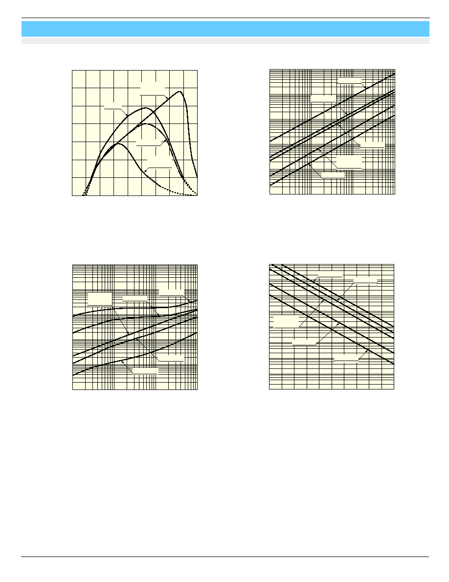
Spectral response characteristics for these Si photodiodes can be selected to meet your application, from among the visible range, visible to near
IR range, and visible to infrared range. Two active areas of 1.3 ◊ 1.3 mm and 2.4 ◊ 2.8 mm are also available.
S5493-01 and S5627-01 provide a spectral response characteristic similar to the visible range sensitivity without using visual-compensated filters.
Features
l S5493-01, S5627-01: Visible range (Filterless type)
l S4797-01, S6931 : Visible to near IR range
l S2833-01, S4011-02: Visible to infrared range
Applications
l Exposure meter
l Illuminometer
l Camera auto exposure
l Stroboscope light control
l Copier
l Display light control
l Optical switch
P H O T O D I O D E
Si photodiode
Photodiodes molded into clear plastic packages
s
General ratings / Absolute maximum ratings
Absolute maximum ratings
Active area
size
Effective
active area
Reverse
voltage
V
R
Max.
Operating
temperature
Topr
Storage
temperature
Tstg
Type No.
Dimensional
outline/
Window
material *
(mm)
(mm
2
)
(V)
(įC)
(įC)
S5493-01
/R
2.4 ◊ 2.8
6.6
S5627-01
/R
1.3 ◊ 1.3
1.6
S6931
/R
2.4 ◊ 2.8
6.6
S4797-01
/R
1.3 ◊ 1.3
1.6
S2833-01
/R
2.4 ◊ 2.8
6.6
S4011-02
/R
1.3 ◊ 1.3
1.6
10
-25 to +85
-40 to +100
* Window material R: clear resin coating
s
Electrical and optical characteristics (Typ. Ta=25 įC, unless otherwise noted)
Photo sensitivity
S
(A/W)
Spectral
response
range
Peak
sensitivity
wavelength
p
p
GaP
LED
He-Ne
laser
Infrared
sensitivity
ratio
Short
circuit
current
Isc
100 lx
Temp.
coefficient
of
Isc
Dark
current
I
D
V
R
=1 V
Max.
Temp.
coefficient
of
I
D
T
CID
Rise
time
tr
V
R
=0 V
R
L
=1 k
Terminal
capacitance
Ct
V
R
=0 V
f=10 kHz
Shunt
resistance
Rsh
V
R
=10 mV
Type No.
(nm)
(nm)
560 nm 633 nm
(%)
(ĶA) (%/įC) (pA) (times/įC) (Ķs)
(pF)
Min.
(G)
Typ.
(G)
S5493-01
1.0
100
10
3000 0.1 1
S5627-01
320 to
840
540
0.3
0.28
0.2
35
0.25
0.25
50
1.13
2
700 0.5 5
S6931
0.48
0.4
0.45
4.2
0.5
200
S4797-01
320 to
1000
720
0.4
0.37
1.2
20
0.2
50
50
S2833-01
6.5
2.5
700
100
S4011-02
320 to
1100
960
0.58
0.33
0.38
-
1.9
0.1
10
1.12
0.5
200
10
250
Si photodiode
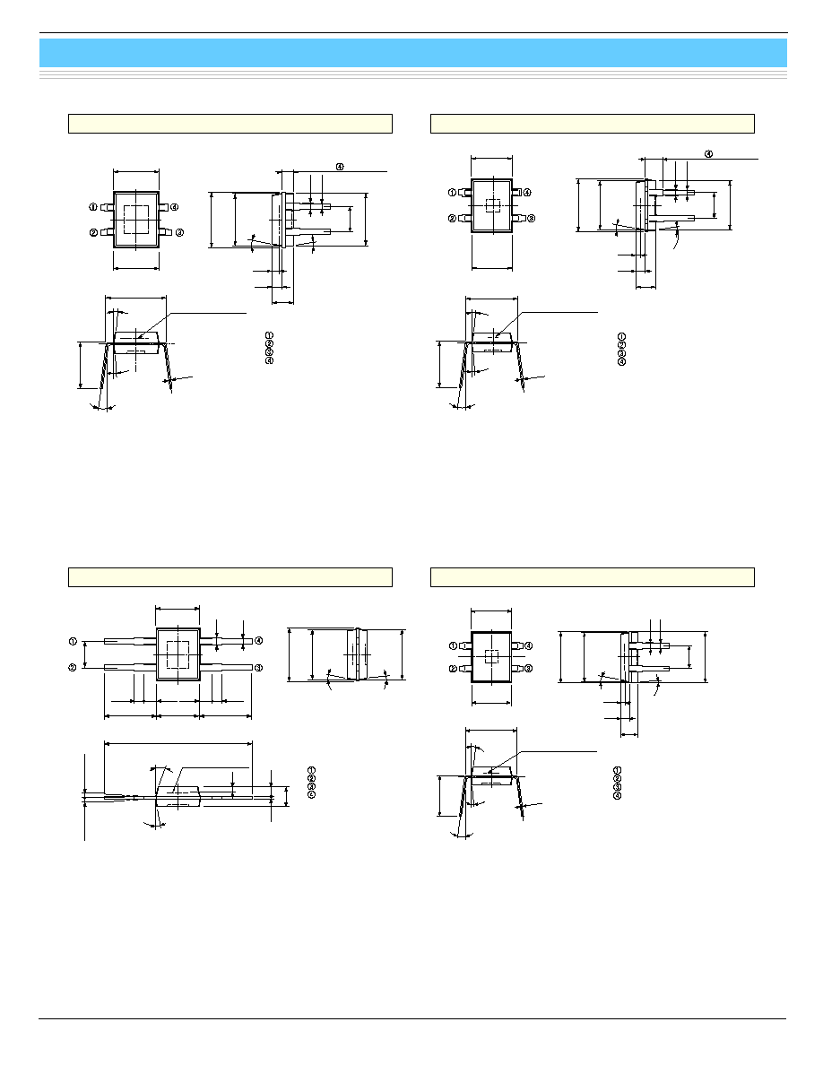
S5493-01, etc.
4.1 Ī 0.2
(INCLUDING BURR)
4.0 *
5.2 Ī 0.2
0.25
10į
7.5 Ī 5į
4.5 Ī 0.4
5.0 Ī 0.2
(INCLUDING BURR)
4.7 *
10
į
4.8 *
2.54
0.5
0.6
5
į
1.8
0.8
0.4
5į
NC
CATHODE
ANODE
CATHODE
PHOTOSENSITIVE
SURFACE
Chip position accuracy with
respect to the package
dimensions marked *
X, Y
Ī0.2
Ī2į
NC
CATHODE
ANODE
CATHODE
4.6 Ī 0.2
(INCLUDING BURR)
4.5 *
5.0 Ī 0.4
5.0 Ī 0.4
(1.0)
(1.0)
14.5 Ī 0.3
(0.8)
0.7
0.5
5.6 Ī 0.2
(INCLUDING BURR)
0.3 MAX.
0.3 MAX.
5į
1.0
0.25
2.0
3į
5.4 *
10
į
5.5 *
3
į
2.54
(0.8)
0.6
PHOTOSENSITIVE
SURFACE
Chip position accuracy with
respect to the package
dimensions marked *
X, Y
Ī0.2
Ī2į
S6931
S4797-01
S5493-01
S5627-01
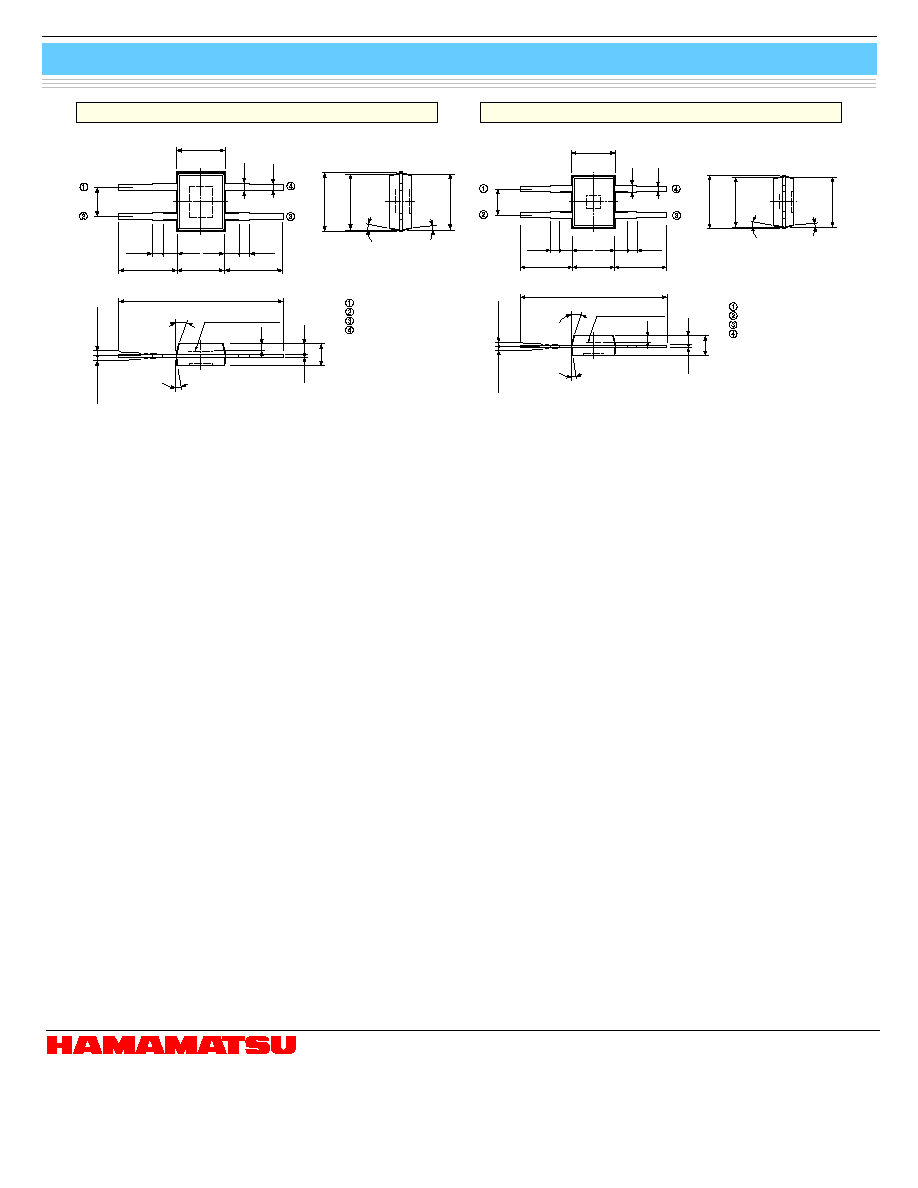
s
s
s
s
s
Dimensional outlines (unit: mm, tolerance unless otherwise noted: Ī0.1 mm)
4.6 Ī 0.2
(INCLUDING BURR)
4.5 *
5.6 Ī 0.2
(INCLUDING BURR)
5.4 *
10
į
3
į
5.5 *
PHOTOSENSITIVE
SURFACE
0.6
1.0
2.0
CATHODE
SUB
ANODE
SUB (SHORT LEAD)
5į
5.75 Ī 0.2
3į
Chip position accuracy with
respect to the package
dimensions marked *
X, Y
Ī0.2
Ī2į
SUB terminal should be
open-circuited at use.
2.54
0.5
0.7
0.25
7.5 Ī 5į
4.5 Ī 0.4
1.0 Ī 0.4 ( PIN LEAD)
KSPDA0118EA
KSPDA0119EA
KSPDA0121EA
KSPDA0122EA
0.25
7.5 Ī 5į
4.5 Ī 0.4
2.54
0.5
0.6
4.1 Ī 0.2
(INCLUDING BURR)
4.0 *
5.0 Ī 0.2
(INCLUDING BURR)
4.7 *
10
į
5
į
4.8 *
0.4
0.8
1.8
CATHODE
SUB
ANODE
SUB (SHORT LEAD)
10į
5.2 Ī 0.2
5į
PHOTOSENSITIVE
SURFACE
Chip position accuracy with
respect to the package
dimensions marked *
X, Y
Ī0.2
Ī2į
SUB terminal should be
open-circuited at use.
1.6 Ī 0.4 ( PIN LEAD)
Si photodiode
S5493-01, etc.
HAMAMATSU PHOTONICS K.K., Solid State Division
1126-1 Ichino-cho, Hamamatsu City, 435-8558 Japan, Telephone: (81) 053-434-3311, Fax: (81) 053-434-5184, http://www.hamamatsu.com
U.S.A.: Hamamatsu Corporation: 360 Foothill Road, P.O.Box 6910, Bridgewater, N.J. 08807-0910, U.S.A., Telephone: (1) 908-231-0960, Fax: (1) 908-231-1218
Germany: Hamamatsu Photonics Deutschland GmbH: Arzbergerstr. 10, D-82211 Herrsching am Ammersee, Germany, Telephone: (49) 08152-3750, Fax: (49) 08152-2658
France: Hamamatsu Photonics France S.A.R.L.: 8, Rue du Saule Trapu, Parc du Moulin de Massy, 91882 Massy Cedex, France, Telephone: 33-(1) 69 53 71 00, Fax: 33-(1) 69 53 71 10
United Kingdom: Hamamatsu Photonics UK Limited: 2 Howard Court, 10 Tewin Road, Welwyn Garden City, Hertfordshire AL7 1BW, United Kingdom, Telephone: (44) 1707-294888, Fax: (44) 1707-325777
North Europe: Hamamatsu Photonics Norden AB: Smidesvšgen 12, SE-171 41 Solna, Sweden, Telephone: (46) 8-509-031-00, Fax: (46) 8-509-031-01
Italy: Hamamatsu Photonics Italia S.R.L.: Strada della Moia, 1/E, 20020 Arese, (Milano), Italy, Telephone: (39) 02-935-81-733, Fax: (39) 02-935-81-741
Information furnished by HAMAMATSU is believed to be reliable. However, no responsibility is assumed for possible inaccuracies or omissions.
Specifications are subject to change without notice. No patent rights are granted to any of the circuits described herein. ©2001 Hamamatsu Photonics K.K.
NC
CATHODE
ANODE
CATHODE
4.1 Ī 0.2
(INCLUDING BURR)
4.0 *
4.9 Ī 0.4
4.9 Ī 0.4
(1.25)
(1.25)
13.8 Ī 0.3
(0.8)
0.6
0.5
5.0 Ī 0.2
(INCLUDING BURR)
0.3 MAX.
0.3 MAX.
10į
0.8
0.25
1.8
5į
4.7 *
10
į
4.8 *
5
į
2.54
(0.8)
0.5
PHOTOSENSITIVE
SURFACE
Chip position accuracy with
respect to the package
dimensions marked *
X, Y
Ī0.2
Ī2į
NC
CATHODE
ANODE
CATHODE
4.6 Ī 0.2
(INCLUDING BURR)
4.5 *
5.0 Ī 0.4
5.0 Ī 0.4
(1.0)
(1.0)
14.5 Ī 0.3
(0.8)
0.7
0.5
5.6 Ī 0.2
(INCLUDING BURR)
0.3 MAX.
0.3 MAX.
5į
1.0
0.25
2.0
3į
5.4 *
10
į
5.5 *
3
į
2.54
(0.8)
0.7
PHOTOSENSITIVE
SURFACE
Chip position accuracy with
respect to the package
dimensions marked *
X, Y
Ī0.2
Ī2į
S2833-01
S4011-02
KSPDA0060EA
KSPDA0123EA
Cat. No. KSPD1025E01
Apr. 2001 DN