
S7565 and S7805-10 amplify the photocurrents generated in the photodiode and provide adequate output current equal to that
obtained from large active area photodiodes. These photo ICs can be used in a wide range of applications involving visible light
detection.
Features
l Visible light detection
l S7565 : Amplifies photocurrents about 1,300 times
S7805-10: Amplifies photocurrents about 13,000 times
l Just as easy to use as a photodiode
Applications
l Energy saving sensor for TV and air conditioners, etc.
P H O T O I C
Photo IC diode
Linear current amplification photo IC for visible range
S7565, S7805-10
s
Absolute maximum ratings (Ta=25 ∞C)
Parameter
Symbol
S7565
S7805-10
Unit
Reverse voltage
V
R
Max.
-0.5 to +16
V
Photocurrent
I
L
10
mA
Forward current
I
F
10
mA
Power dissipation
P
250 *
150 *
mW
Operating temperature
Topr
-10 to +60
∞C
Storage temperature
Tstg
-20 to +70
∞C
Soldering
-
260 ∞C, 3 s, at least 3.6 mm away
from package surface
260 ∞C, 3 s, at least 1.8 mm away
from package surface
-
*1: Derate power dissipation at a rate of 3.3 mW/∞C above Ta=25 ∞C
*2: Derate power dissipation at a rate of 2.0 mW/∞C above Ta=25 ∞C
s
Electrical and optical characteristics (Ta=25 ∞C, V
4
=5 V)
S7565
S7805-10
Parameter
Symbol
Condition
Min.
Typ.
Max.
Min.
Typ.
Max.
Unit
Spectral response range
l
-
350 to 750
-
-
350 to 750
-
nm
Peak sensitivity wavelength
lp
-
560
-
-
560
-
nm
Operating reverse voltage
V
R
3
-
12
3
-
12
V
Dark current
I
D
-
0.5
10
-
5
100
nA
Photocurrent
I
L
2856 K, 1000 lx
0.24
0.32
0.4
2.25
3
3.75
mA
Rise time
tr
-
0.6
-
-
6
-
ms
Fall time
tf
10 to 90 %, R
L
=10 k9
l=560 nm
-
0.6
-
-
6
-
ms
s Rise/fall time measurement method
PULSED LIGHT
FROM LED
(
=560 nm)
V
O
LOAD
RESISTANCE R
L
7.5 V
90 %
2.5 V
10 %
V
O
tr
tf
0.1 µF
KPICC0053EA
1
HAMAMATSU PHOTONICS K.K., Solid State Division
1126-1 Ichino-cho, Hamamatsu City, 435-8558 Japan, Telephone: (81) 053-434-3311, Fax: (81) 053-434-5184, http://www.hamamatsu.com
U.S.A.: Hamamatsu Corporation: 360 Foothill Road, P.O.Box 6910, Bridgewater, N.J. 08807-0910, U.S.A., Telephone: (1) 908-231-0960, Fax: (1) 908-231-1218
Germany: Hamamatsu Photonics Deutschland GmbH: Arzbergerstr. 10, D-82211 Herrsching am Ammersee, Germany, Telephone: (49) 08152-3750, Fax: (49) 08152-2658
France: Hamamatsu Photonics France S.A.R.L.: 8, Rue du Saule Trapu, Parc du Moulin de Massy, 91882 Massy Cedex, France, Telephone: 33-(1) 69 53 71 00, Fax: 33-(1) 69 53 71 10
United Kingdom: Hamamatsu Photonics UK Limited: 2 Howard Court, 10 Tewin Road, Welwyn Garden City, Hertfordshire AL7 1BW, United Kingdom, Telephone: (44) 1707-294888, Fax: (44) 1707-325777
North Europe: Hamamatsu Photonics Norden AB: Smidesv‰gen 12, SE-171 41 Solna, Sweden, Telephone: (46) 8-509-031-00, Fax: (46) 8-509-031-01
Italy: Hamamatsu Photonics Italia S.R.L.: Strada della Moia, 1/E, 20020 Arese, (Milano), Italy, Telephone: (39) 02-935-81-733, Fax: (39) 02-935-81-741
Information furnished by HAMAMATSU is believed to be reliable. However, no responsibility is assumed for possible inaccuracies or omissions.
Specifications are subject to change without notice. No patent rights are granted to any of the circuits described herein. ©2001 Hamamatsu Photonics K.K.
Cat. No. KPIC1040E01
Jan. 2001 DN
Photo IC diode
S7565, S7805-10
0.01
100
LOAD RESISTANCE (
)
RISE/F
ALL TIME
(ms)
1 k
10 k
100 k
1 M
(Typ. Ta=25 ∞C, V
R
=5 V,
=560 nm, Vo=2.5 V)
1
0.1
10
100
S7565
S7805-10
100 fA
-25
AMBIENT TEMPERATURE (∞C)
D
ARK CURRENT
0
25
50
75
100
(Typ. V
R
=5 V)
1 nA
100 pA
10 pA
1 pA
10 nA
100 nA
1 mA
10 mA
S7565
S7805-10
0
200
WAVELENGTH (nm)
RELA
TIVE SENSITIVITY
400
600
800
1000
(Typ. Ta=25 ∞C, V
R
=5 V)
0.2
0.4
0.6
0.8
1.0
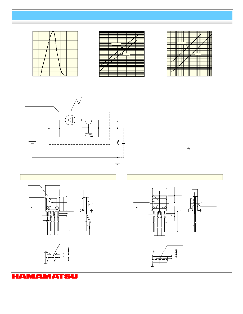
s Dark current temperature characteristics s Rise/fall time vs. load resistance
KPICB0041EA
KPICB0040EA
s Spectral response
KPICB0039EA
CATHODE
THE DRAWING SURROUNDED
BY THE DOTTED LINE SHOWS
A SCHEMATIC DIAGRAM OF
THE PHOTO IC.
LOAD CAPACITANCE C
L
FOR LOW-PASS FILTER
R
L
REVERSE
BIAS
POWER
SUPPLY
ANODE
LOAD
RESISTANCE
s Operating circuit example
s Dimensional outlines (unit: mm)
S7565
S7805-10
5.2 ± 0.3
(INCLUDING BURR)
CENTER OF
ACTIVE AREA
VISUAL-
COMPENSATION
FILTER
(2.6 ◊ 3.9 ◊ 0.5 t)
5.2 ± 0.3
(INCLUDING BURR)
(SPECIFIED AT THE LEAD OUT)
PHOTOSENSITIVE
SURFACE
ANODE
(ANODE)
NC
CATHODE
2.0
(DEPTH 0.15 MAX.)
1.0
(DEPTH 0.15 MAX.)
2.5 ± 0.2
5.0
2.02 ± 0.2
5.0
16.5 ± 1.0
(0.8)
(1.0)
1.27 1.27 1.27
(1.27)
10∞
5∞
0.75 ± 0.15
10
∞
5
∞
3.6 MAX.
0.25
+0.15
-0.1
0.55
0.45
1.0
2.0
Pin be connected to
on the PC board.
Tolerance unless otherwise
noted: ±0.1, ±2∞
Shaded area indicates burr.
Values in parentheses are not
guaranteed, but for reference.
5.2 ± 0.3
(INCLUDING BURR)
CENTER OF
ACTIVE AREA
VISUAL-
COMPENSATION
FILTER
(4.6 ◊ 3.4 ◊ 0.5 t)
5.2 ± 0.3
(INCLUDING BURR)
(SPECIFIED AT THE LEAD OUT)
PHOTOSENSITIVE
SURFACE
ANODE
(ANODE)
NC
CATHODE
2.0
(DEPTH 0.15 MAX.)
1.0
(DEPTH 0.15 MAX.)
2.5 ± 0.2
5.0
2.02 ± 0.2
5.0
1.4 MAX.
8.3 ± 0.5
(0.8)
(1.0)
1.27 1.27 1.27
10∞
5∞
0.75 ± 0.15
10
∞
5
∞
0.25
+0.15
-0.1
0.55
0.45
1.0
2.0
Tolerance unless otherwise
noted: ±0.1, ±2∞
Shaded area indicates burr.
Values in parentheses are not
guaranteed, but for reference.
KPICA0025EA
KPICA0040EA
KPICC0018EA
Connect a bias power supply so that
a positive voltage is applied to the
cathode. To remove high-frequency
components from the circuit, we rec-
ommend inser ting a load capaci-
tance (C
L
) for low-pass filter, in par-
allel with a load resistance (R
L
). The
cut-off frequency (fc) is then given by
Cut-off frequency (fc)
2
C
L
R
L
1
2