Features
Applications
I M A G E S E N S O R
CCD area image sensor
Back-thinned FFT-CCD for high-speed application
S7960/S7961-1008
S7960/S7961-1008 are FFT-CCD area image sensors specifically designed for high speed operation. A high frame rate is attained by employing
a wide band width on-chip amplifier. In binning operation, S7960/S7961-1008 can be used as a linear image sensor having a long aperture in the
direction of the device length. The binning operation offers significant improvement in signal-to-noise ratio and signal processing speed compared
to conventional methods by which signals are digitally added by an external circuit. In area scan operation, S7960/S7961-1008 can be used as a
high frame rate camera. S7960/S7961-1008 also feature low dark signal (MPP mode operation). S7960/S7961-1008 have an effective pixel size
of 24 ◊ 24 µm and is available in image areas of 24.576 (H) ◊ 6.000 (V) mm.
One-stage peltier cooler is built into the package for thermoelectric cooling (S7961-1008). At room temperature operation, the device can be
cooled down to -10 ∞C (Typ.) without using any other cooling technique. In addition, since both the CCD chip and the peltier cooler are
hermetically sealed, no dry air is required, thus allowing easy handling.
I Selection and order guide
Type No.
Cooling
Number of
total pixels
Number of
active pixels
Active area
[mm (H) ◊ mm (V)]
S7960-1008
Non-cooled
S7961-1008
One-stage TE-cooled
1044 ◊ 256
1024 ◊ 250
24.576 ◊ 6.000
A window material can be selected upon need, and the following is available.
AR-coated sapphire (standard): expressed by S #
Quart: expressed by Q #
Temporary window: expressed by N #
# This should be added at the end of a type No. when ordered.
ex. S7960-1008S: AR-coated sapphire
I General ratings
Parameter
Specification
CCD structure
Full frame transfer
Fill factor
100 %
Number of active pixels
1024 (H) ◊ 250 (V)
Pixel size
24 (H) ◊ 24 (V) µm
Active area
24.576 (H) ◊ 6.000 (V) mm
Vertical clock phase
2 phase
Horizontal clock phase
2 phase
Output circuit
Two-stage MOSFET source follower
Package
24 pin ceramic package
Window
AR coated sapphire
Quartz, temporary window are available upon request
G High-speed on-chip amplifier
G Greater than 90 % quantum efficiency
G Wide spectral response range
G Built-in TE-cooler
G MPP operation
G Non-cooled type: S7960-1008
One-stage TE-cooled type: S7961-1008
(Two-stage TE-cooled type is optional)
G High-speed spectrometer
G High-speed UV imaging
G Optical and spectrophotometric analyzer
1
CCD area image sensor
S7960/S7961-1008
I Absolute maximum ratings (Ta=25 ∞C)
Parameter
Symbol
Min.
Typ.
Max.
Unit
Operating temperature
Topr
-50
-
+30
∞C
Storage temperature
Tstg
-50
-
+70
∞C
OD voltage
V
OD
-0.5
-
+25
V
RD voltage
V
RD
-0.5
-
+18
V
ISV voltage
V
ISV
-0.5
-
+18
V
ISH voltage
V
ISH
-0.5
-
+18
V
IGV voltage
V
IG1V
, V
IG2V
-10
-
+15
V
IGH voltage
V
IG1H
, V
IG2H
-10
-
+15
V
SG voltage
V
SG
-10
-
+15
V
OG voltage
V
OG
-10
-
+15
V
RG voltage
V
RG
-10
-
+15
V
TG voltage
V
TG
-10
-
+15
V
Vertical clock voltage
V
P1V
, V
P2V
-10
-
+15
V
Horizontal clock voltage
V
P1H
, V
P2H
-10
-
+15
V
I Operating conditions (MPP mode, Ta=25 ∞C)
Parameter
Symbol
Min.
Typ.
Max.
Unit
Output transistor drain voltage
V
OD
12
15
18
V
Reset drain voltage
V
RD
11.5
12
12.5
V
Output gate voltage
V
OG
1
3
5
V
Substrate voltage
V
SS
-
0
-
V
Test point (vertical input source)
V
ISV
-
V
RD
-
V
Test point (horizontal input source)
V
ISH
-
V
RD
-
V
Test point (vertical input gate)
V
IG1V
, V
IG2V
-8
0
-
V
Test point (horizontal input gate)
V
IG1H
, V
IG2H
-8
0
-
V
High
V
P1VH
, V
P2VH
4
6
8
Vertical shift register
clock voltage
Low
V
P1VL
, V
P2VL
-9
-8
-7
V
High
V
P1HH
, V
P2HH
4
6
8
Horizontal shift register
clock voltage
Low
V
P1HL
, V
P2HL
-9
-8
-7
V
High
V
SGH
4
6
8
Summing gate voltage
Low
V
SGL
-9
-8
-7
V
High
V
RGH
4
6
8
Reset gate voltage
Low
V
RGL
-9
-8
-7
V
High
V
TGH
4
6
8
Transfer gate voltage
Low
V
TGL
-9
-8
-7
V
I Electrical characteristics (Ta=25 ∞C)
Parameter
Symbol
Remark
Min.
Typ.
Max.
Unit
Signal output frequency
fc
-
-
1
10
MHz
Reset clock frequency
frg
-
-
1
10
MHz
Vertical shift register capacitance
C
P1V
, C
P2V
-
-
6,400
-
pF
Horizontal shift register capacitance
C
P1H
, C
P2H
-
-
300
-
pF
Summing gate capacitance
C
SG
-
-
7
-
pF
Reset gate capacitance
C
RG
-
-
7
-
pF
Transfer gate capacitance
C
TG
-
-
150
-
pF
Transfer efficiency
CTE
*
1
0.99995
0.99999
-
-
DC output level
Vout
*
2
7
10
13
V
Output impedance
Zo
*
2
-
500
-
W
Power dissipation
P
*
2,
*
3
-
100
-
mW
*1: Charge transfer efficiency per pixel, measured at half of the full well capacity.
*2: V
OD
=15 V, Load resistance=2.2 kW
*3: Power dissipation of the on-chip amplifier.
2
CCD area image sensor
S7960/S7961-1008
I Electrical and optical characteristics (Ta=25 ∞C, unless otherwise noted)
Parameter
Symbol
Remark
Min.
Typ.
Max.
Unit
Saturation output voltage
Vsat
-
Fw ◊ Sv
-
V
Vertical
150
300
-
Full well
capacity
Horizontal
Fw
*
4
150
300
-
ke-
CCD node sensitivity
Sv
*
5
1.8
2.2
-
µV/e-
25 ∞C
-
4,000
12,000
Dark current
(MPP mode)
0 ∞C
DS
*
6
-
200
600
e-/pixel/s
Readout noise
Nr
*
7
-
60
120
e-rms
Line binning
1,250
5,000
-
Dynamic range
Area scanning
DR
*
8
1,250
5,000
-
-
Spectral response range
l
-
-
200 to 1,100
-
nm
Photo response non-uniformity
PRNU
*
9
-
-
±10
%
*4: Large horizontal full well for line binning operation.
*5: V
OD
=15 V , Load resistance=2.2 kW
*6: Dark current nearly doubles for every 5 to7 ∞C increase in temperature.
*7: -40 ∞C, operating frequency is 1 MHz.
*8: DR = Fw / Nr
*9: Measured at half of the full well capacity.
PRNU (%) = noise / signal ◊ 100
Noise: fixed pattern noise (peak to peak)
I Pin connections
S7960 series
S7961 series
Pin
No.
Symbol
Description
Symbol
Description
Remark
1
RD
Reset drain
RD
Reset drain
2
OS
Output transistor source
OS
Output transistor source
3
OD
Output transistor drain
OD
Output transistor drain
4
OG
Output gate
OG
Output gate
5
SG
Summing gate
SG
Summing gate
Same timing as P2H
6
NC
NC
7
NC
NC
8
P2H
CCD horizontal register clock-2
P2H
CCD horizontal register clock-2
9
P1H
CCD horizontal register clock-1
P1H
CCD horizontal register clock-1
10
IG2H
Test point (horizontal input gate-2)
IG2H
Test point (horizontal input gate-2)
Shorted to 0 V
11
IG1H
Test point (horizontal input gate-1)
IG1H
Test point (horizontal input gate-1)
Shorted to 0 V
12
ISH
Test point (horizontal input source)
ISH
Test point (horizontal input source)
Shorted to RD
13
TG
Transfer gate
TG
Transfer gate
Same timing as P2V *
10
14
P2V
CCD vertical register clock-2
P2V
CCD vertical register clock-2
15
P1V
CCD vertical register clock-1
P1V
CCD vertical register clock-1
16
NC
Th1
Thermistor
17
NC
Th2
Thermistor
18
NC
P-
TE-cooler-
19
NC
P+
TE-cooler+
20
SS
Substrate (GND)
SS
Substrate (GND)
21
ISV
Test point (vertical input source)
ISV
Test point (vertical input source)
Shorted to RD
22
IG2V
Test point (vertical input gate-2)
IG2V
Test point (vertical input gate-2)
Shorted to 0 V
23
IG1V
Test point (vertical input gate-1)
IG1V
Test point (vertical input gate-1)
Shorted to 0 V
24
RG
Reset gate
RG
Reset gate
*10: TG is an isolation gate between vertical register and horizontal resister.
In standard operation, the same pulse of P2V should be applied to the TG.
3
CCD area image sensor
S7960/S7961-1008
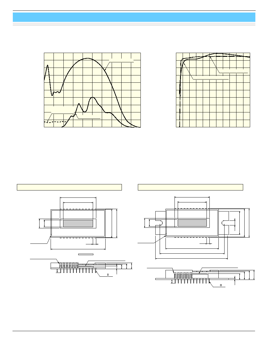
QUANTUM EFFICIENCY (%)
WAVELENGTH (nm)
(Typ. Ta=25 ∞C)
0
200
400
600
800
1000
1200
10
20
30
40
50
60
70
80
90
100
FRONT-SIDED
FRONT-SIDED
(UV COAT)
BACK-THINNED
KMPDB0058EA
I Spectral response without window
0
10
100 200
WAVELENGTH (nm)
TRANSMITTANCE (%)
300 400 500 600 700 800 900 1000 1100 1200
20
30
40
50
60
70
80
90
100
(Typ. Ta=25 ∞C)
QUARTZ WINDOW
AR COATED SAPPHIRE
KMPDB0110EA
KMPDA0106EA
3.0
PHOTOSENSITIVE SURFACE
4.0
2.4
4.8
3.4
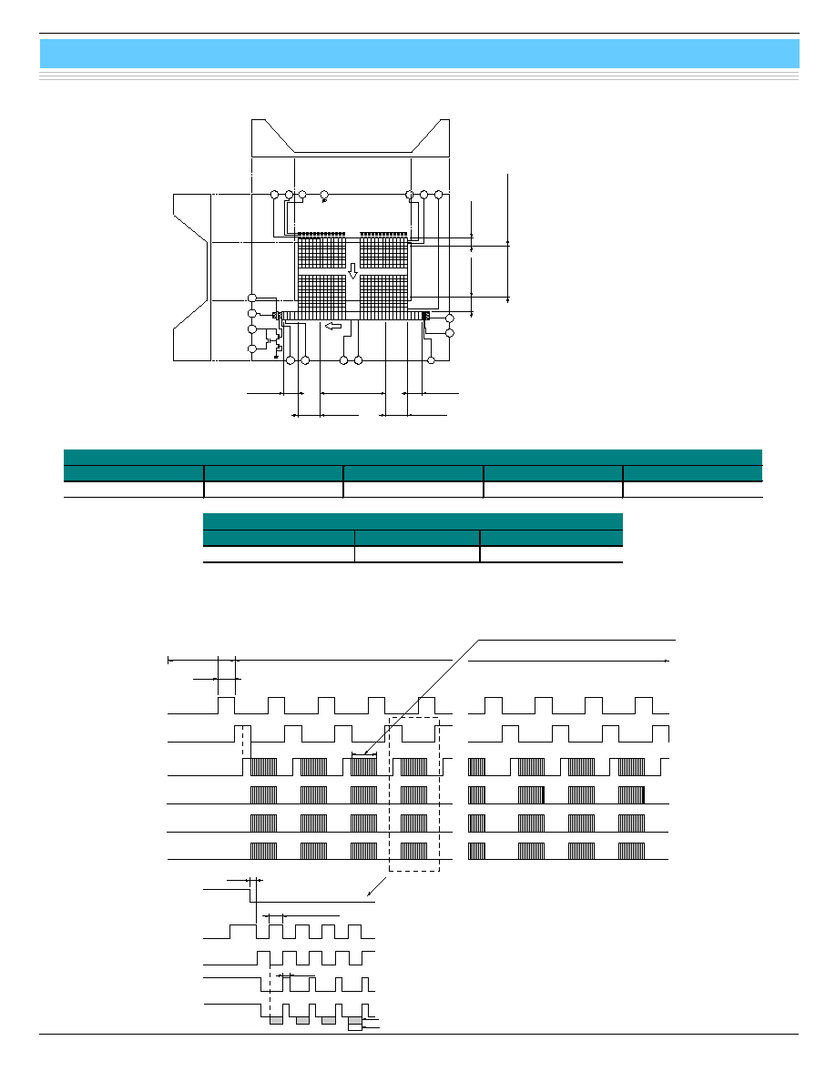
WINDOW 28.6
22.9
22.4
ACTIVE AREA 24.576
6.000
8.2
44.0
2.54
1st PIN INDEX MARK
(24 ◊) 0.5
1 2
24 23
INDEX MARK
(24 ◊) 0.5
6.9
1.0
3.0
6.3
4.8
PHOTOSENSITIVE SURFACE
7.7
1st PIN INDEX MARK
6.000
4.0
19.0
22.4
22.9
44.0
52.0
60.0
2.54
WINDOW 28.6
ACTIVE AREA 24.576
8.2
TE-COOLER
1 2
24 23
INDEX MARK
KMPDA0105EA
I Dimensional outlines (unit: mm)
I Spectral transmittance characteristic
of window material
S7960-1008
S7961-1008
4
CCD area image sensor
S7960/S7961-1008
KMPDC0096EA
I Device structure, line output format
23
22
21
20
14
15
1
3
11
9
2 BEVEL
250 SIGNAL OUT
4 BLANK
4 BLANK
V=250
H=1024
4 BEVEL
THINNING
THINNING
1 2 3 4 5
2
3
4
5
V
H
6 BEVEL
1024
SIGNAL OUT
13
10
6 BEVEL
24
4
5
8
12
2
...
...
...
...
...
...
Pixel format
Left ¨ Horizontal direction Æ Right
Blank
Bevel
Effective
Bevel
Blank
4
6
1024
6
4
Top ¨ Vertical direction Æ Bottom
Bevel
Effective
Bevel
2
250
4
KMPDC0097EA
I Timing chart
G Area scanning 1 (low dark current mode)
P1V
P2V
TG
P1H
P2H, SG
RG
Vos
P1H
P2H, SG
RG
Vos
INTEGRATION PERIOD
(Shutter must be opened)
Tpwv
READOUT PERIOD
(Shutter must be closed)
1
2
3
EXPANDED VIEW
DARK SIGNAL
PHOTO GENERATED SIGNAL
D1
D2
1 HORIZONTAL-SCANNING READOUT PERIOD
P2V
TG
Tovr
Tpwh, Tpws
Tpwr
5
CCD area image sensor
S7960/S7961-1008
Parameter
Symbol
Remark
Min.
Typ.
Max.
Unit
Pulse width
Tpwv
11
-
-
µs
P1V, P2V, TG
Rise and fall time
Tprv, Tpfv
*
20
-
-
ns
Pulse width
Tpwh
50
-
-
ns
Rise and fall time
Tprh, Tpfh
10
-
-
ns
P1H, P2H
Duty ratio
-
*
-
50
-
%
Pulse width
Tpws
50
-
-
ns
Rise and fall time
Tprs, Tpfs
10
-
-
ns
SG
Duty ratio
-
-
-
50
-
%
Pulse width
Tpwr
15
-
-
ns
RG
Rise and fall time
Tprr, Tpfr
-
5
-
-
ns
TG P1H
Overlap time
Tovr
-
3
-
-
µs
*11: Symmetrical pulses should be overlapped at 50 % of maximum amplitude.
KMPDC0104EA
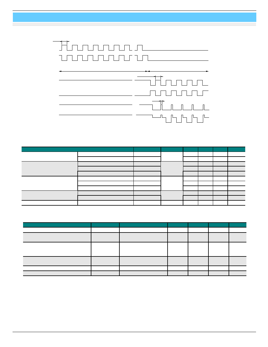
G Area scanning 2 (large full well mode)
P1V
P2V
TG
P1H
P2H, SG
RG
Vos
P1H
P2H, SG
RG
Vos
1
2
3
EXPANDED VIEW
Tpwr
DARK SIGNAL
PHOTO GENERATED SIGNAL
D1
D2
1 HORIZONTAL-SCANNING READOUT PERIOD
P2V
TG
Timing Chart: Area Scanning 2 (S7960/S7961 Serie )
INTEGRATION PERIOD
(Shutter must be opened)
Tpwv
READOUT PERIOD
(Shutter must be closed)
Tovr
Tpwh, Tpws
Parameter
Symbol
Remark
Min.
Typ.
Max.
Unit
Pulse width
Tpwv
11
-
-
µs
P1V, P2V, TG
Rise and fall time
Tprv, Tpfv
*
20
-
-
ns
Pulse width
Tpwh
50
-
-
ns
Rise and fall time
Tprh, Tpfh
10
-
-
ns
P1H, P2H
Duty ratio
-
*
-
50
-
%
Pulse width
Tpws
50
-
-
ns
Rise and fall time
Tprs, Tpfs
10
-
-
ns
SG
Duty ratio
-
-
-
50
-
%
Pulse width
Tpwr
15
-
-
ns
RG
Rise and fall time
Tprr, Tpfr
-
5
-
-
ns
TG P1H
Overlap time
Tovr
-
3
-
-
µs
*12: Symmetrical pulses should be overlapped at 50 % of maximum amplitude.
6
CCD area image sensor
S7960/S7961-1008
KMPDC0017EA
G Line binning
P1V
P2V
P1H
P2H, SG
RG
Vos
LINE BINNING PERIOD
D1
D2
TG
READOUT PERIOD
Tpwv
Tpwh, Tpws
Tpwr
Parameter
Symbol
Remark
Min.
Typ.
Max.
Unit
Pulse width
Tpwv
11
-
-
µs
P1V, P2V, TG
Rise and fall time
Tprv, Tpfv
*
!
20
-
-
ns
Pulse width
Tpwh
50
-
-
ns
Rise and fall time
Tprh, Tpfh
10
-
-
ns
P1H, P2H
Duty ratio
-
*
!
-
50
-
%
Pulse width
Tpws
50
-
-
ns
Rise and fall time
Tprs, Tpfs
10
-
-
ns
SG
Duty ratio
-
-
-
50
-
%
Pulse width
Tpwr
15
-
-
ns
RG
Rise and fall time
Tprr, Tpfr
-
5
-
-
ns
TG P1H
Overlap time
Tovr
-
3
-
-
µs
*13: Symmetrical pulses should be overlapped at 50 % of maximum amplitude.
I Specifications of built-in TE-cooler (S7961-1008)
Parameter
Symbol
Condition
Min.
Typ.
Max.
Unit
Internal resistance
Rint
Ta=27 ∞C
-
1.2
-
W
Maximum current *
"
Imax
Th *
#
=27 ∞C
DT *
$
= DTmax
-
-
3.0
A
Maximum voltage
Vmax
Th *
#
=27 ∞C
DT = DTmax
I = Imax
-
-
3.6
V
Maximum heat absorption *
%
Qmax
Tc *
&
=Th *
#
=27 ∞C
I=Imax
-
-
5.0
W
Maximum temperature at hot side
-
-
-
70
∞C
CCD temperature
-
Ta=25 ∞C
-
-10
0
∞C
*14: If the current is greater than Imax, the heat absorption begins to decrease due to the Joule heat. It should be noted that this
value is not a damage threshold. To protect the thermoelectric cooler and maintain stable operation, the supply current
should be less than 60 % of this maximum current.
*15: Temperature at hot side of thermoelectric cooler.
*16: DT = Th - Tc
*17:This is a theoretical heat absorption level that offsets the temperature difference in the TE-cooler element when the
maximum current is supplied to the unit.
*18: Temperature at cool side of thermoelectric cooler.
7
CCD area image sensor
S7960/S7961-1008
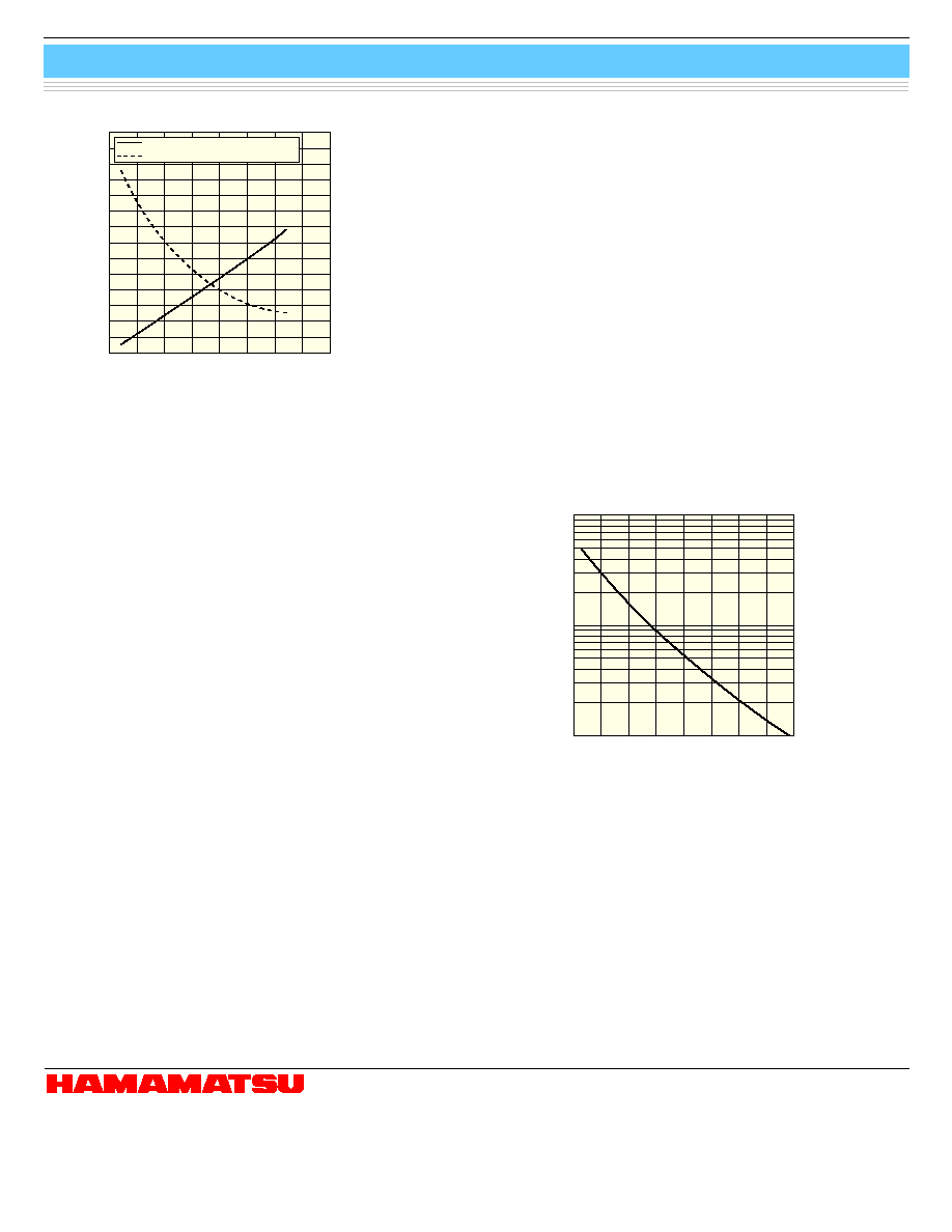
(Typ. Ta=25 ∞C)
10 k
220
240
260
TEMPERATURE (K)
RESIST
ANCE
280
300
100 k
1 M
I Precaution for use (Electrostatic countermeasures)
G Handle these sensors with bare hands or wearing cotton gloves. In addition, wear anti-static clothing or use a wrist band with
an earth ring, in order to prevent electrostatic damage due to electrical charges from friction.
G Avoid directly placing these sensors on a work-desk or work-bench that may carry an electrostatic charge.
G Provide ground lines or ground connection with the work-floor, work-desk and work-bench to allow static electricity to dis-
charge.
G Ground the tools used to handle these sensors, such as tweezers and soldering irons.
It is not always necessary to provide all the electrostatic measures stated above. Implement these measures according to the
amount of damage that occurs.
I Heating/cooling rate
The heating/cooling rate should be set at less than 5 K/min.
I Specifications of built-in temperature sensor (S7961-1008)
A chip thermistor is built in the same package with a CCD chip, and the CCD chip temperature can be monitored with it. A relation
between the thermistor resistance and absolute temperature is expressed by the following equation.
R1 = R2 ◊ expB (1 / T1 - 1 / T2)
where R1 is the resistance at absolute temperature T1 (K)
R2 is the resistance at absolute temperature T2 (K)
B is so-called the B constant (K)
The characteristics of the thermistor used are as follows.
R (298K) = 10 kW
B (298K / 323K) = 3450 K
KMPDB0111EA
HAMAMATSU PHOTONICS K.K., Solid State Division
1126-1 Ichino-cho, Hamamatsu City, 435-8558 Japan, Telephone: (81) 053-434-3311, Fax: (81) 053-434-5184, http://www.hamamatsu.com
U.S.A.: Hamamatsu Corporation: 360 Foothill Road, P.O.Box 6910, Bridgewater, N.J. 08807-0910, U.S.A., Telephone: (1) 908-231-0960, Fax: (1) 908-231-1218
Germany: Hamamatsu Photonics Deutschland GmbH: Arzbergerstr. 10, D-82211 Herrsching am Ammersee, Germany, Telephone: (49) 08152-3750, Fax: (49) 08152-2658
France: Hamamatsu Photonics France S.A.R.L.: 8, Rue du Saule Trapu, Parc du Moulin de Massy, 91882 Massy Cedex, France, Telephone: 33-(1) 69 53 71 00, Fax: 33-(1) 69 53 71 10
United Kingdom: Hamamatsu Photonics UK Limited: 2 Howard Court, 10 Tewin Road, Welwyn Garden City, Hertfordshire AL7 1BW, United Kingdom, Telephone: (44) 1707-294888, Fax: (44) 1707-325777
North Europe: Hamamatsu Photonics Norden AB: Smidesv‰gen 12, SE-171 41 Solna, Sweden, Telephone: (46) 8-509-031-00, Fax: (46) 8-509-031-01
Italy: Hamamatsu Photonics Italia S.R.L.: Strada della Moia, 1/E, 20020 Arese, (Milano), Italy, Telephone: (39) 02-935-81-733, Fax: (39) 02-935-81-741
Information furnished by HAMAMATSU is believed to be reliable. However, no responsibility is assumed for possible inaccuracies or omissions.
Specifications are subject to change without notice. No patent rights are granted to any of the circuits described herein. ©2003 Hamamatsu Photonics K.K.
Cat. No. KMPD1034E07
Feb. 2003 DN
0
1
2
3
V
OL
T
A
GE (V)
CCD TEMPERA
TURE
(
∞
C)
4
7
6
5
-40
-30
4
3
2
CURRENT (A)
1
0
-20
-10
0
10
20
30
(Typ. Ta=25 ∞C)
VOLTAGE vs. CURRENT
CCD TEMPERATURE vs. CURRENT
KMPDB0179EA
8