
S8040 is a light modulation photo IC consisting of a dual photodiode and a control/processing circuit integrated on a single chip. When used with
an infrared LED and light emitting/receiving lenses, S8040 detects the distance (near or far) to an object based on a prespecified distance by
utilizing the triangular distance measurement method. S8040 can be operated in 2 modes: self-running mode and single trigger mode. Current
consumption during standby (no distance detection) is held to 20 ĶA Max. Average current consumption is minimized by setting a longer
measurement cycle.
Self-running mode: Operates with a measurement cycle proportional to the external capacitor value. (250 ms Typ. at 0.1 ĶF)
Single trigger mode: Detects the distance only when a trigger pulse is input to the TRIG terminal.
P H O T O I C
PRELIMINARY DATA
Jan. 2002
S8040
Photo IC for rangefinder
Photo IC for far/near detection (with energy saving mode)
Features
l
Detects distance (far/near) to object
l
Energy saving operation
l
Operation mode switching function
l
Visible-cut plastic package impervious to background light
l
Miniature plastic package
Applications
l
Optical switch
s Absolute maximum ratings (Ta=25 įC)
Parameter
Symbol
Value
Unit
Supply voltage
Vcc
-0.5 to +7.0
V
Output voltage
Vo
-0.5 to Vcc+0.5
V
Output current
Io
150
ĶA
E xternal cap acitor term ina l voltage
V
CEXT
-0.5 to Vcc+0.5
V
Trigger terminal voltage
V
TRIG
-0.5 to Vcc+0.5
V
LED terminal voltage
V
LED
-0.5 to Vcc+0.5
V
Power dissipation
P
250 *
mW
Operating temperature
Topr
-20 to +70
įC
Storage temperature
Tstg
-30 to +80
įC
Soldering
-
230 įC, 3 s
-
* Derate power dissipation at a rate of -3.3 mW/įC above Ta=25 įC
s Electrical and optical characteristics (Ta=25 įC, Vcc=5 V, unless otherwise noted)
Parameter
Symbol
Condition
Min.
Typ.
Max.
Unit
Peak sensitivity wavelength
p
-
850
-
nm
Photo sensitivity
S
=900 nm
-
0.3
-
A/W
Supply voltage
Vcc
4
5
6
V
C urrent consum ption during m easurem ent
Icc
-
3
5
mA
C urrent consum ption during standby
I
STB
No background light
-
-
20
ĶA
High level LED output voltage
V
LEDH
Source 10 mA
1.2
1.4
1.6
V
Low level LED output voltage
V
LEDL
LED terminal open
-
-
0.3
V
High level LED pulse width
Tw
4.6
7
10.5
Ķs
Measurement time
TS
Self-running, single trigger
69
105
158
Ķs
Measurement cycle
TB
Self-running, Cext=0.1 ĶF
150
250
350
ms
T hreshold input differential current
I
TH
No background light
2.5
5
10
nA
Allowable background light
Ex
Between channels < 500 lx
3000
-
-
lx
Low level output voltage
Vol
Sink 100 ĶA
-
-
0.2
V
High level output voltage
Voh
Source 100 ĶA
2.2
-
-
V
1
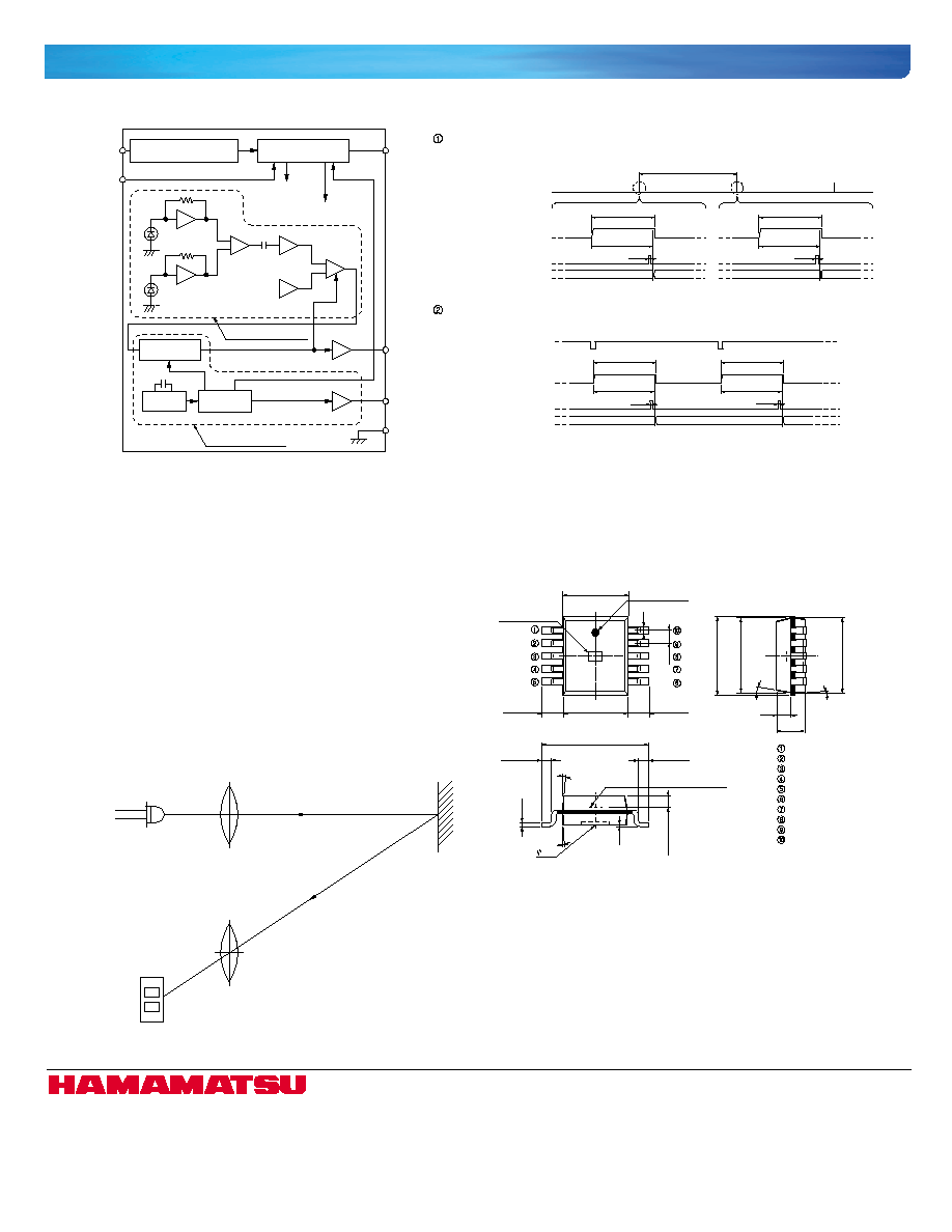
Photo IC for rangefinder
S8040
HAMAMATSU PHOTONICS K.K., Solid State Division
1126-1 Ichino-cho, Hamamatsu City, 435-8558 Japan, Telephone: (81) 053-434-3311, Fax: (81) 053-434-5184, http://www.hamamatsu.com
U.S.A.: Hamamatsu Corporation: 360 Foothill Road, P.O.Box 6910, Bridgewater, N.J. 08807-0910, U.S.A., Telephone: (1) 908-231-0960, Fax: (1) 908-231-1218
Germany: Hamamatsu Photonics Deutschland GmbH: Arzbergerstr. 10, D-82211 Herrsching am Ammersee, Germany, Telephone: (49) 08152-3750, Fax: (49) 08152-2658
France: Hamamatsu Photonics France S.A.R.L.: 8, Rue du Saule Trapu, Parc du Moulin de Massy, 91882 Massy Cedex, France, Telephone: 33-(1) 69 53 71 00, Fax: 33-(1) 69 53 71 10
United Kingdom: Hamamatsu Photonics UK Limited: 2 Howard Court, 10 Tewin Road, Welwyn Garden City, Hertfordshire AL7 1BW, United Kingdom, Telephone: (44) 1707-294888, Fax: (44) 1707-325777
North Europe: Hamamatsu Photonics Norden AB: Smidesvšgen 12, SE-171 41 Solna, Sweden, Telephone: (46) 8-509-031-00, Fax: (46) 8-509-031-01
Italy: Hamamatsu Photonics Italia S.R.L.: Strada della Moia, 1/E, 20020 Arese, (Milano), Italy, Telephone: (39) 02-935-81-733, Fax: (39) 02-935-81-741
Information furnished by HAMAMATSU is believed to be reliable. However, no responsibility is assumed for possible inaccuracies or omissions.
Specifications are subject to change without notice. No patent rights are granted to any of the circuits described herein. ©2002 Hamamatsu Photonics K.K.
Cat. No. KPIC1029E02
Jan. 2002 DN
Self-running mode
(Capacitor of 0.1 ĶF Typ. is connected between CEXT and GND. TRIG is fixed to High level.)
Single trigger mode
(CEXT is shorted to GND. Low level pulse with at least 20 Ķs width is applied to TRIG.)
SUPPLY CURRENT
SUPPLY CURRENT
LED TERMINAL VOLTAGE
OUT TERMINAL VOLTAGE
TRIG TERMINAL VOLTAGE
SUPPLY CURRENT
LED TERMINAL VOLTAGE
OUT TERMINAL VOLTAGE
T
B
I
CC
I
STB
I
STB
105 Ķs
116 Ķs
116 Ķs
116 Ķs
116 Ķs
7 Ķs
I
CC
I
STB
I
STB
I
STB
105 Ķs
7 Ķs
I
CC
105 Ķs
7 Ķs
I
CC
I
STB
I
STB
105 Ķs
7 Ķs
INFRARED LED
PD2
PD1
PHOTO IC FOR
RANGEFINDER
LIGHT EMITTING LENS
LIGHT RECEIVING LENS
S8040 incorporates a dual photodiode (0.5 ◊ 0.7 mm active
area per channel) and a control/processing integrated circuit.
When used with an infrared LED and light emitting/receiving
lenses, S8040 detects the distance (near or far) to an object
based on a prespecified distance by utilizing the triangular
distance measurement method.
When making optical design, photodiode 2 of the dual photo-
diode in the photo IC for rangefinder must be set closer to the
infrared LED as shown below.
s
Block diagram
CONSTANT
VOLTAGE CIRCUIT
RELAXIZATION
ASCILLATION CIRCUIT
ANALOG CIRCUIT
POWER SUPPLY
DIGITAL CIRCUIT
POWER SUPPLY
GND
NOTE 1) Terminal polarity
TRIG: Starts measurement at Low level
LED: LED is driven at High level
OUT: Changes to High level when signal is input
NOTE 2) CEXT and TRIG should be TTL input
LED
OUT
Vcc
CEXT
TRIG
PREAMP
PREAMP
DIFFERENTIAL BUFFER
COMPARATOR
OUTPUT CIRCUIT
LED OUTPUT
REF. VOLTAGE (HYSTERISIS)
PD1
PD2
SYNC
DETECTION CIRCUIT
TIMING
GENERATOR
ANALOG CIRCUIT
DIGITAL CIRCUIT
OSCILLATION
CIRCUIT
KPICC0056EB
s
Timing chart: consecutive measurements
KPICC0057EB
s
Functions and optical systems
KPICC0065EA
s
Dimensional outline (unit: mm)
0.89
0.4
4.6 Ī 0.2
(INCLUDING BURR)
PD1
(NEAR)
PD2
(FAR)
1.5 Ī 0.4
1.5 Ī 0.4
4.5 *
7.5 Ī 0.3
0.7 Ī 0.3
0.7 Ī 0.3
0.25
0.1
3į
5į
0.75 Ī 0.15
2.0
5.5 *
5.6 Ī 0.2
(INCLUDING BURR)
3į
2.0
1.0
5.4 *
10į
Tolerance unless otherwise
noted: Ī0.1, Ī2į
Shaded area indicates burr.
Chip position accuracy with
respect to the package
dimensions marked *
X, Y
Ī0.2,
G
Ī2į
Vcc
CEXT
TRIG
NC
OUT
GND
NC
NC
NC
LED
ACTIVE AREA
(2 ◊) 0.5 ◊ 0.7
INDEX MARK:
WHITE
PHOTOSENSITIVE
SURFACE
KPICA0031EB
2