Hamamatsu provides various types of Si PIN photodiodes molded into clear plastic packages. These photodiodes are available with cut-off
frequencies from 60 MHz to 500 MHz, allowing you to make the selection that best suits your application. S8387 offers high sensitivity in the violet
region and is suited for violet laser detection.
Features
l
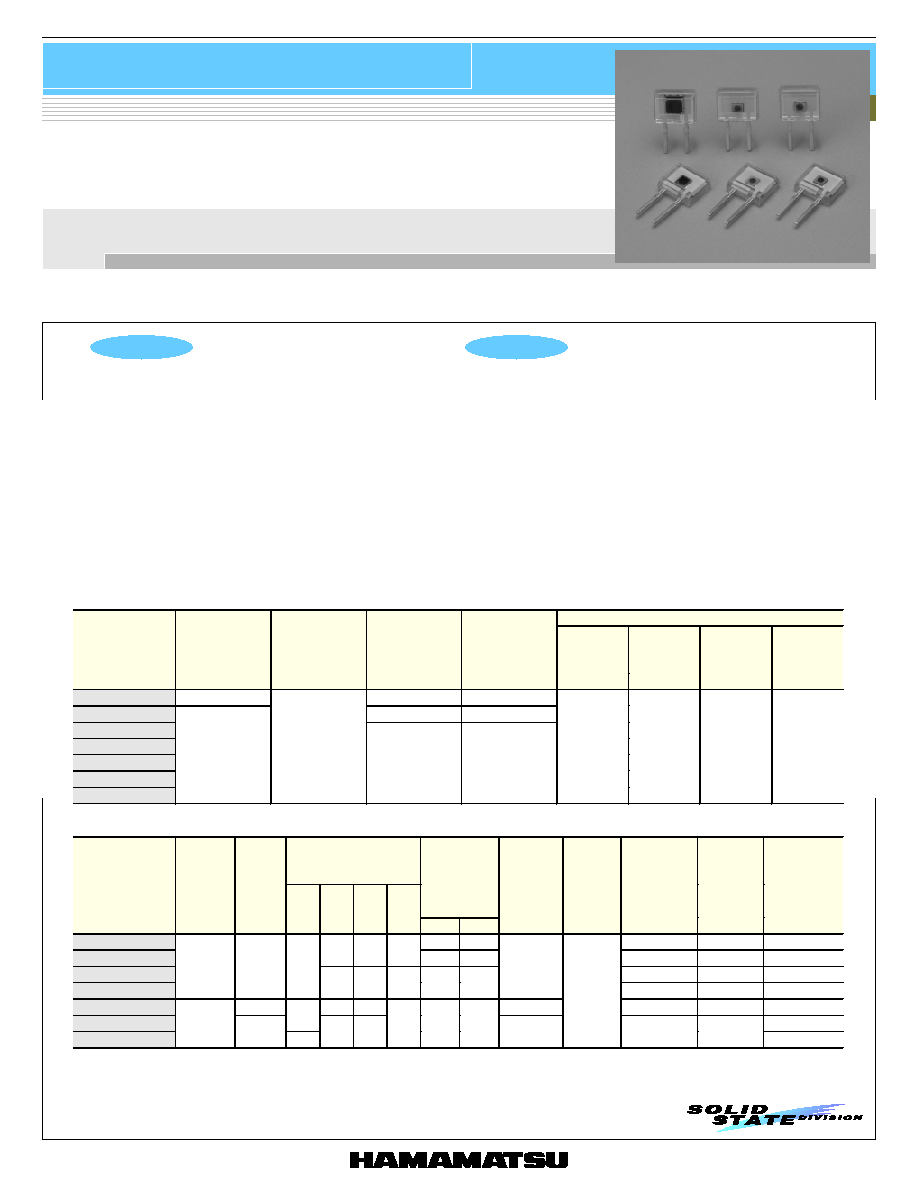
Clear plastic package (4 ◊ 4.8 mm)
l
2-pin lead style (lead length: 4.9 mm)
l
Choice of cut-off frequencies
Applications
l
Laser diode front monitors (high-speed APC) for optical
disk drives
l
Red laser diode (650 nm) and near IR laser diode (780 nm)
sensors
l
Violet laser detection (S8387)
P H O T O D I O D E
Si PIN photodiode
Available with 60 MHz to 500 MHz response speeds
Plastic package
1
s General ratings / Absolute maximum ratings
Absolute maximum ratings
Active area
size
Effective active
area
Reverse
voltage
V
R
Max.
Power
dissipation
P
Operating
te m p erature
Topr
Storage
te m p erature
Tstg
Type No.
Dimensional
outline
Package
(mm)
(mm
2
)
(V)
(mW)
(∞C)
(∞C)
S7329-01
2 ◊ 2
4
S7836
1.1 ◊ 1.1
1.2
S3321-04
S8223
S8314
S7762
S8387
Plastic
0.8
0.5
20
50
-25 to +85
-40 to +100
s Electrical and optical characteristics (Typ. Ta=25 ∞C, unless otherwise noted)
Photo sensitivity
S
(A/W)
Spectral
response
range
Peak
sensitivity
wavelength
p
Short circuit
current
lsc
100 lx
(µA)
Dark
current
I
D
Max.
Temp.
coefficient
of
I
D
T
CID
Cut-off
frequency
fc
=780 nm
R
L
=50
, -3dB
T er mi nal
capacitance
Ct
f=1 MHz
NEP
=
p
Type No.
(nm)
(nm)
410
nm
660
nm
780
nm
830
nm
Min.
Typ.
(nA)
(ti m es/∞ C)
(MHz)
(pF)
(W/Hz
1/2
)
S7329-01
3.3
4.2
60 *
1
12 *
1
4.8 ◊ 10
-15
*
1
S7836
0.45 0.55 0.6
1.3
1.65
70 *
1
5 *
1
3.9 ◊ 10
-15
*
1
S3321-04
80 *
1
3 *
1
4.1 ◊ 10
-15
*
1
S8223
320 to
1060
900
0.19
0.39 0.48 0.5
0.6
0.75
1 *
1
200 *
1
3 *
1
3.4 ◊ 10
-15
*
1
S8314
800
0.39 0.45
0.3 *
1
500 *
1
4 *
1
3.9 ◊ 10
-15
*
1
S7762
0.2
1.4 ◊ 10
-15
*
2
S8387
320 to
1000
760
0.27
0.48 0.5
0.45 0.37
0.5
0.3 *
2
1.15
500 *
2
6 *
2
1.6 ◊ 10
-15
*
2
*1: V
R
=5 V
*2: V
R
=2.5 V

HAMAMATSU PHOTONICS K.K., Solid State Division
1126-1 Ichino-cho, Hamamatsu City, 435-8558 Japan, Telephone: (81) 053-434-3311, Fax: (81) 053-434-5184, http://www.hamamatsu.com
U.S.A.: Hamamatsu Corporation: 360 Foothill Road, P.O.Box 6910, Bridgewater, N.J. 08807-0910, U.S.A., Telephone: (1) 908-231-0960, Fax: (1) 908-231-1218
Germany: Hamamatsu Photonics Deutschland GmbH: Arzbergerstr. 10, D-82211 Herrsching am Ammersee, Germany, Telephone: (49) 08152-3750, Fax: (49) 08152-2658
France: Hamamatsu Photonics France S.A.R.L.: 8, Rue du Saule Trapu, Parc du Moulin de Massy, 91882 Massy Cedex, France, Telephone: 33-(1) 69 53 71 00, Fax: 33-(1) 69 53 71 10
United Kingdom: Hamamatsu Photonics UK Limited: 2 Howard Court, 10 Tewin Road, Welwyn Garden City, Hertfordshire AL7 1BW, United Kingdom, Telephone: (44) 1707-294888, Fax: (44) 1707-325777
North Europe: Hamamatsu Photonics Norden AB: Smidesv‰gen 12, SE-171 41 Solna, Sweden, Telephone: (46) 8-509-031-00, Fax: (46) 8-509-031-01
Italy: Hamamatsu Photonics Italia S.R.L.: Strada della Moia, 1/E, 20020 Arese, (Milano), Italy, Telephone: (39) 02-935-81-733, Fax: (39) 02-935-81-741
Information furnished by HAMAMATSU is believed to be reliable. However, no responsibility is assumed for possible inaccuracies or omissions.
Specifications are subject to change without notice. No patent rights are granted to any of the circuits described herein. ©2002 Hamamatsu Photonics K.K.
Si PIN photodiode
Plastic package
Cat. No. KPIN1053E02
Jan. 2002 DN
1 pF
10 pF
100 pF
0.1
1
10
100
REVERSE VOLTAGE (V)
TERMINAL CAPACITANCE
(Typ. Ta=25 ∞C, f=1 MHz)
S7329-01
S3321-04
S8314
S8223
S7836
S8387, S7762
100 fA
1 pA
10 pA
100 pA
0.01
0.1
1
10
100
REVERSE VOLTAGE (V)
DARK CURRENT
(Typ. Ta=25 ∞C)
S7329-01
S7836
S3321-04
S8314
S8223
S8387
S7762
0
0.1
0.2
0.3
0.4
0.7
200
400
600
800
1000
WAVELENGTH (nm)
PHOTO SENSITIVITY
(A/W)
(Typ. Ta=25 ∞C)
0.5
0.6
QE=100 %
S7836, S7329-01
S3321-04
S8223
10
100
1000
1
10
100
REVERSE VOLTAGE (V)
CUT-OFF FREQUENCY (MHz)
(Typ. Ta=25 ∞C,
=780 nm, R
L
=50
)
S8314
S8387
S7762
S8223
S3321-04
S7836
S7329-01
5.0 MAX.
(INCLUDING BURR)
CENTER OF
ACTIVE AREA
4.2 ± 0.2
(INCLUDING BURR)
4.7 *
4.9 ± 0.25
(0.8)
(1.25)
0.45
2.54
(2
◊
) 10
∞
(2
◊
) 5
∞
0.25
0.5
0.5
0.4
0.8
1.8
4.0 *
PHOTOSENSITIVE
SURFACE
(2 ◊) 10
∞
(2 ◊) 5
∞
0.5
PHOTOSENSITIVE
SURFACE
Chip position accuracy with respect
to the package dimensions marked *
X, Y
±0.2
±2∞
5.0 MAX.
(INCLUDING BURR)
CENTER OF
ACTIVE AREA
4.2 ± 0.2
(INCLUDING BURR)
4.7 *
4.9 ± 0.25
(0.8)
(1.25)
2.54
(2
◊
) 10
∞
(2
◊
) 5
∞
0.25
a
0.5
0.4
0.8
1.8
4.0 *
PHOTOSENSITIVE
SURFACE
(2 ◊) 10∞
(2 ◊) 5∞
PHOTOSENSITIVE
SURFACE
Chip position accuracy with respect
to the package dimensions marked *
X, Y
±0.2
±2∞
S7836
S3321-04
S8223
S8314
S7762
S8387
a
0.5
0.4
0
0.1
0.2
0.3
0.4
0.7
200
400
600
800
1000
WAVELENGTH (nm)
PHOTO SENSITIVITY
(A/W)
0.5
0.6
(Typ. Ta=25 ∞C)
S8314
QE=100 %
S8387
S7762
KPINA0052EA
s
Spectral response (1)
KPINB0185EA
s
Dark current vs. reverse voltage
KPINB0186EA
s
Cut-off frequency vs. reverse voltage
KPINB0242EA
s
Terminal capacitance vs. reverse voltage
KPINB0188EA
s
Dimensional outlines (unit: mm, tolerance unless otherwise noted: ±0.1)
KPINA0085EB
s
Spectral response (2)
KPINB0189EA
S7329-01
S7836, S3321-04, S8223, S8314, S7762, S8387
2