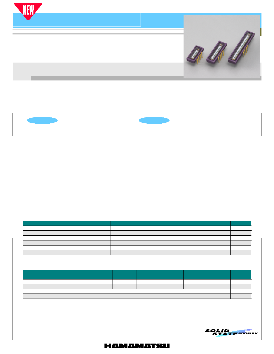
S8377/S8378 series
Features
l Wide active area
Pixel pitch: 50 µm (S8377 series)
25 µm (S8378 series)
Pixel height: 0.5 mm
l On-chip charge amplifier with excellent input/output
characteristics
l Built-in timing generator allows operation with only
start and clock pulse inputs
l Maximum operating clock frequency: 500 kHz
l Spectral response range: 200 to 1000 nm
l Single 5 V power supply operation
l 8-pin small package, S8377 and S8378 series are pin
compatible.
Applications
l Image input devices
l Optical sensing devices
I M A G E S E N S O R
CMOS linear image sensor
Built-in timing generator and signal processing circuit; single 5 V supply operation
S8377/S8378 series is a family of CMOS linear image sensors designed for image input applications. These linear image sensors operate from
single 5 V supply with only start and clock pulse inputs, making them easy to use. The signal processing circuit has a charge amplifier with
excellent input/output characteristics and allows signal readout at 500 kHz.
The photodiodes of S8377 series have a height of 0.5 mm and are arrayed in a row at a spacing of 50 µm. The photodiodes of S8378 series also
have a height of 0.5 mm but are arrayed at a spacing of 25 µm. The photodiodes are available in 3 different pixel quantities for each series: 128
(S8377-128Q), 256 (S8377-256Q, S8378-256Q), 512 (S8377-512Q, S8378-512Q) and 1024 (S8378-1024Q). Quartz glass is the standard window
material.
1
I Absolute maximum ratings
Parameter
Symbol
Value
Unit
Supply voltage
Vdd
-0.3 to +10
V
Gain selection terminal voltage
Vg
-0.3 to +10
V
Clock pulse voltage
V (CLK)
-0.3 to +10
V
Start pulse voltage
V (ST)
-0.3 to +10
V
Operating temperature *
1
Topr
-20 to +60
∞C
Storage temperature
Tstg
-20 to +80
∞C
*1: No condensation
I Shape specifications
Parameter
S8377-
128Q
S8377-
256Q
S8377-
512Q
S8378-
256Q
S8378-
512Q
S8378-
1024Q
Unit
Number of pixels
128
256
512
256
512
1024
-
Package length
15.8
22.2
35.0
15.8
22.2
35.0
mm
Number of pins
8
8
-
Window material
Quartz
Quartz
-
CMOS linear image sensor
S8377/S8378 series
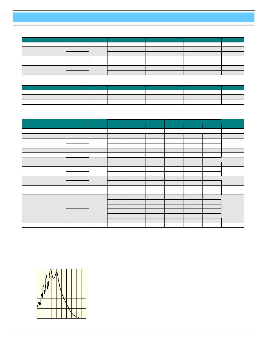
WAVELENGTH (nm)
RELATIVE SENSITIVITY (%)
200
400
0
40
20
1200
(Typ. Ta=25 ∞C)
100
80
60
1000
800
600
2
I Spectral response (typical example)
KMPDB0213EA
I Recommended terminal voltage
Parameter
Symbol
Min.
Typ.
Max.
Unit
Supply voltage
Vdd
4.75
5
5.25
V
High gain
0
-
0.4
V
Gain selection
terminal voltage
Low gain
Vg
Vdd-0.25
Vdd
Vdd+0.25
V
High
Vdd-0.25
Vdd
Vdd+0.25
V
Clock pulse voltage
Low
V (CLK)
0
-
0.4
V
High
Vdd-0.25
Vdd
Vdd+0.25
V
Start pulse voltage
Low
V (ST)
0
-
0.4
V
I Electrical characteristics
Parameter
Symbol
Min.
Typ.
Max.
Unit
Clock pulse frequency *
2
f (CLK)
0.1
-
500
kHz
Output impedance
Zo
-
1
-
k
Power consumption
P
-
25
-
mW
*2: Ta=25 ∞C, Vdd=5 V, V (CLK)=V (ST)=5 V, Vg=5 V (Low gain)
I Electrical and optical characteristics [Ta=25 ∞C, Vdd=5 V, V (CLK)=V (ST)=5 V]
S8377 series
S8378 series
Parameter
Symbol
Min.
Typ.
Max.
Min.
Typ.
Max.
Unit
Spectral response range
200 to 1000
200 to 1000
nm
Peak sensitivity wavelength
p
-
500
-
-
500
-
nm
High gain
-
22
-
-
22
-
Photo sensitivity
Low gain
S
-
4.4
-
-
4.4
-
V/lx
∑
s
Dark current
I
D
-
0.08
0.24
-
0.04
0.12
pA
Saturation charge
Qsat
-
12.5
-
-
6.3
-
pC
High gain
-
1
-
-
0.5
-
F e e d b a c k c a p acitanc e *
3
of charg e a m plifier
Low gain
Cf
-
5
-
-
2.5
-
PF
High gain
-
8.0
24
-
8.0
24
Dark output voltage *
4
Low gain
Vd
-
1.6
4.8
-
1.6
4.8
MV
High gain
2.8
3.2
-
2.8
3.2
-
Saturation output
voltage
Low gain
Vsat
2.1
2.5
-
2.1
2.5
-
V
High gain
-
145
-
-
145
-
Saturation exposure *
5
Low gain
Esat
-
570
-
-
570
-
mlx
∑
s
-
0.1 (-128 Q)
-
-
0.2 (-256 Q)
-
-
0.15 (-256 Q)
-
-
0.3 (-512 Q)
-
Low gain
-
0.2 (-512 Q)
-
-
0.4 (-1024 Q)
-
-
0.4 (-128 Q)
-
-
0.9 (-256 Q)
-
-
0.5 (-256 Q)
-
-
1.3 (-512 Q)
-
Readout noise
High gain
Nr
-
0.8 (-512 Q)
-
-
2.1 (-1024 Q)
-
mV-rms
Photo response non-uniformity *
6
PRNU
-
-
±3
-
-
±3
%
*3: Vg=5 V (Low gain), Vg=0 V (High gain)
*4: Storage time Ts=100 ms
*5: Measured with a tungsten lamp of 2856 K.
*6: Uniformity is defined under the condition that the device is uniformly illuminated by light which is 50 % of the saturation
exposure level as follows:
PRNU=
X/X ◊ 100 (%)
Where X is the average output of all pixels and
X is the difference from the maximum or minimum output and X.

CMOS linear image sensor
S8377/S8378 series
I Timing chart
KMPDC0149EA
3
Parameter
Symbol
Min.
Typ.
Max.
Unit
Start pulse width
tpw (ST)
600
-
-
ns
Start pulse rise and fall time
tr (ST), tf (ST)
0
20
30
ns
Clock pulse width
tpw (CLK)
1000
-
-
ns
Clock pulse rise and fall time
tr (CLK), tf (CLK)
0
20
30
ns
Clock pulse-start pulse timing
t (CLK-ST)
400
-
-
ns
Video delay time 1
tvd1
-
300
-
ns
Video delay time 2
tvd2
-
150
-
ns
STORAGE TIME
1
ST
CLK
Video
ST
CLK
Video
EOS
2
n-1
n
tf (ST)
t (CLK-ST)
tpw (CLK)
tvd1
tr (ST)
tr (CLK)
tf (CLK)
tvd2
tpw (ST)
* The storage time is determined by the start pulse intervals. However, since the charge
storage of each pixel is carried out between the signal readout of that pixel and the next
signal readout of the same pixel, the start time of charge storage differs depending on each
pixel. In addition, the next start pulse cannot be input until signal readout from all pixels is
completed.
Vout
CMOS linear image sensor
S8377/S8378 series
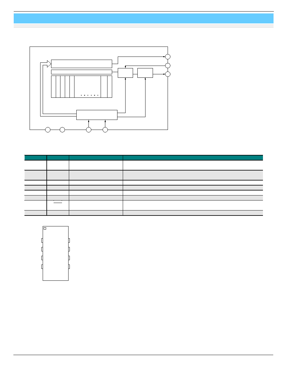
I Block diagram
KMPDC0150EA
I Pin connections
Pin No.
Symbol
Name of pin
Function
1
CLK
Clock pulse
Pulse input to operate the shift register. The readout time (data rate)
equals the clock pulse frequency.
2
ST
Start pulse
Starts the shift register operation. The start pulse intervals determine the
signal storage time.
3
Vg
Gain selection voltage
Input of 5 V selects "Low gain" and 0 V selects "High gain"
4
Vdd
Supply voltage
5 V Typ.
5
NC
Open
6
Video
Video
Signal output. Positive-going output from 1 V
7
EOS
End of scan
Negative-going signal output obtained at a timing following the last pixel
scan.
8
Vss
Ground
4
CHARGE
AMP
CLAMP
CIRCUIT
DIGITAL SHIFT REGISTER
ADDRESS SWITCH
PHOTODIODES
TIMING GENERATOR
1
2
3
4
5
N
N-1
CLK
1
ST
2
Vdd
4
Vss
8
EOS
7
Vg
3
Video
6
CLK
ST
Vg
Vdd
1
2
3
4
Vss
EOS
Video
NC
8
7
6
5
KMPDC0151EA
CMOS linear image sensor
S8377/S8378 series
5
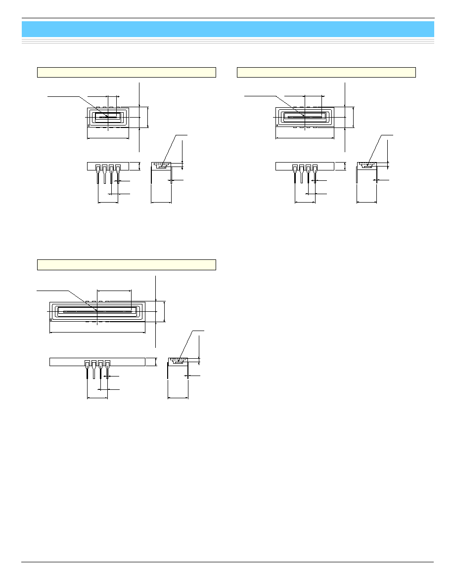
I Dimensional outlines (unit: mm)
KMPDA0150EB
S8377-128Q, S8378-256Q
S8377-256Q, S8378-512Q
KMPDA0151EB
KMPDA0152EB
S8377-512Q, S8378-1024Q
0.51
7.62
2.54
3.0
ACTIVE AREA
6.4 ◊ 0.5
7.87
3.935 ± 0.2
3.935 ± 0.2
3.2 ± 0.3
15.8
* Optical distance from the outer surface
of the quartz window to the chip surface
7.62
1.3 ± 0.2 *
0.25
CHIP
3.0
7.87
3.935 ± 0.2
3.935 ± 0.2
ACTIVE AREA
12.8 ◊ 0.5
6.4 ± 0.3
22.2
7.62
2.54
0.51
* Optical distance from the outer surface
of the quartz window to the chip surface
7.62
1.3 ± 0.2 *
0.25
CHIP
3.0
7.87
3.935 ± 0.2
3.935 ± 0.2
ACTIVE AREA
25.6 ◊ 0.5
12.8 ± 0.3
35.0
7.62
2.54
0.51
* Optical distance from the outer surface
of the quartz window to the chip surface
7.62
1.3 ± 0.2 *
0.25
CHIP

CMOS linear image sensor
S8377/S8378 series
HAMAMATSU PHOTONICS K.K., Solid State Division
1126-1 Ichino-cho, Hamamatsu City, 435-8558 Japan, Telephone: (81) 053-434-3311, Fax: (81) 053-434-5184, http://www.hamamatsu.com
U.S.A.: Hamamatsu Corporation: 360 Foothill Road, P.O.Box 6910, Bridgewater, N.J. 08807-0910, U.S.A., Telephone: (1) 908-231-0960, Fax: (1) 908-231-1218
Germany: Hamamatsu Photonics Deutschland GmbH: Arzbergerstr. 10, D-82211 Herrsching am Ammersee, Germany, Telephone: (49) 08152-3750, Fax: (49) 08152-2658
France: Hamamatsu Photonics France S.A.R.L.: 8, Rue du Saule Trapu, Parc du Moulin de Massy, 91882 Massy Cedex, France, Telephone: 33-(1) 69 53 71 00, Fax: 33-(1) 69 53 71 10
United Kingdom: Hamamatsu Photonics UK Limited: 2 Howard Court, 10 Tewin Road, Welwyn Garden City, Hertfordshire AL7 1BW, United Kingdom, Telephone: (44) 1707-294888, Fax: (44) 1707-325777
North Europe: Hamamatsu Photonics Norden AB: Smidesv‰gen 12, SE-171 41 Solna, Sweden, Telephone: (46) 8-509-031-00, Fax: (46) 8-509-031-01
Italy: Hamamatsu Photonics Italia S.R.L.: Strada della Moia, 1/E, 20020 Arese, (Milano), Italy, Telephone: (39) 02-935-81-733, Fax: (39) 02-935-81-741
Information furnished by HAMAMATSU is believed to be reliable. However, no responsibility is assumed for possible inaccuracies or omissions.
Specifications are subject to change without notice. No patent rights are granted to any of the circuits described herein. ©2002 Hamamatsu Photonics K.K.
Cat. No. KMPD1066E02
Apr. 2002 DN
6
I Handling precautions
(1) Electrostatic countermeasures
Although the CMOS linear image sensor is protected against static electricity, proper electrostatic countermeasures must be
provided to prevent device destruction by static electricity. For example, such measures include wearing non-static gloves
and clothes, and grounding the work area and tools.
(2) Incident window
If the incident window is contaminated or scratched, the output uniformity will deteriorate considerably, so care should be
taken in handling the window. Avoid touching it with bare hands.
The window surface should be cleaned before using the device. If dry cloth or dry cotton swab is used to rub the window
surface, static electricity may be generated, and therefore this practice should be avoided. Use soft cloth, cotton swab or soft
paper moistened with ethyl alcohol to wipe off dirt and foreign matter on the window surface.
(3) UV exposure
The CMOS linear image sensor is designed to suppress performance deterioration due to UV exposure. Even so, avoid
unnecessary UV exposure to the device.
Also, be careful not to allow UV light to strike the cemented portion between the ceramic base and the glass.
(4) Operating and storage environments
Always observe the rated temperature range when handling the device. Operating or storing the device at an excessively
high temperature and humidity may cause variations in performance characteristics and must be avoided.