P H O T O D I O D E
PRELIMINARY DATA
Jan. 2002
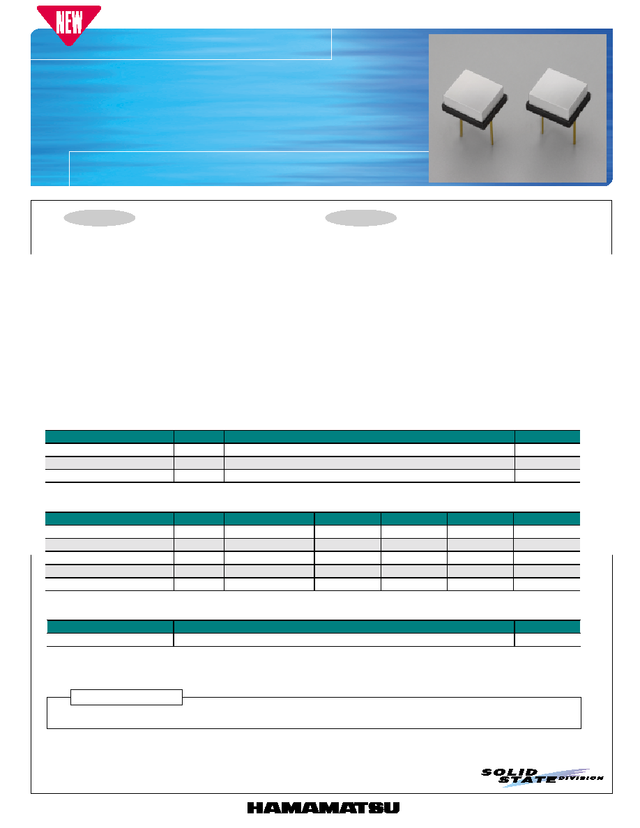
S8559
Si photodiode
Detector for X-ray monitor
Features
l
Si photodiode coupled to low cost CsI scintillator
l
Ideal for detection of X-ray energy below 100 keV
Applications
l
X-ray detection
l
X-ray monitors
s Absolute maximum ratings (Ta=25
∞
C)
Parameter
Symbol
Value
Unit
Reverse voltage
V
R
Max.5
V
Operating temperature
Topr
-10 to +60
∞
C
Storage temperature
Tstg
-20 to +70
∞
C
s Electrical and optical characteristics (without scintillator, Ta=25
∞
C)
Parameter
Symbol
Condition
Min.
Typ.
Max.
Unit
Spectral response range
-
190 to 1000
-
nm
Peak sensitivity wavelength
p
720
-
nm
Photo sensitivity
S
=500 nm
-
0. 26
-
A/W
Dark current
I
D
V
R
=10 mV
-
2
50
pA
Terminal capacitance
Ct
V
R
=0 V, f=10 kHz
-
950
-
pF
s X-ray sensitivity (reference value, tube current: 1.0 mA, aluminum filter: t=6 mm)
X-ray tube voltage
Typ.
Unit
120 kV
100
nA
Note) Depends on equipment and measurement conditions.
Avoid storing or using S8559 at high humidity because CsI scintillator has deliquescence.
Handling precautions
1

Si photodiode
S8559
HAMAMATSU PHOTONICS K.K., Solid State Division
1126-1 Ichino-cho, Hamamatsu City, 435-8558 Japan, Telephone: (81) 053-434-3311, Fax: (81) 053-434-5184, http://www.hamamatsu.com
U.S.A.: Hamamatsu Corporation: 360 Foothill Road, P.O.Box 6910, Bridgewater, N.J. 08807-0910, U.S.A., Telephone: (1) 908-231-0960, Fax: (1) 908-231-1218
Germany: Hamamatsu Photonics Deutschland GmbH: Arzbergerstr. 10, D-82211 Herrsching am Ammersee, Germany, Telephone: (49) 08152-3750, Fax: (49) 08152-2658
France: Hamamatsu Photonics France S.A.R.L.: 8, Rue du Saule Trapu, Parc du Moulin de Massy, 91882 Massy Cedex, France, Telephone: 33-(1) 69 53 71 00, Fax: 33-(1) 69 53 71 10
United Kingdom: Hamamatsu Photonics UK Limited: 2 Howard Court, 10 Tewin Road, Welwyn Garden City, Hertfordshire AL7 1BW, United Kingdom, Telephone: (44) 1707-294888, Fax: (44) 1707-325777
North Europe: Hamamatsu Photonics Norden AB: Smidesv‰gen 12, SE-171 41 Solna, Sweden, Telephone: (46) 8-509-031-00, Fax: (46) 8-509-031-01
Italy: Hamamatsu Photonics Italia S.R.L.: Strada della Moia, 1/E, 20020 Arese, (Milano), Italy, Telephone: (39) 02-935-81-733, Fax: (39) 02-935-81-741
Information furnished by HAMAMATSU is believed to be reliable. However, no responsibility is assumed for possible inaccuracies or omissions.
Specifications are subject to change without notice. No patent rights are granted to any of the circuits described herein. ©2002 Hamamatsu Photonics K.K.
Cat. No. KSPD1051E01
Jan. 2002 DN
10.1 ± 0.1
CsI (TI) 8.9
8.9 ± 0.1
CsI (TI)
7.9
2.0 ± 0.1
(10.5)
2.85
t=3.0
4.85
0.3
9.2 ± 0.3
7.4 ± 0.2
8.0 ± 0.3
ANODE
TERMINAL MARK
0.5
LEAD
PHOTOSENSITIVE
SURFACE
s
Terminal capacitance vs. reverse voltage
s
Dark current vs. reverse voltage
s
Dimensional outline (unit: mm)
100 fA
1 pA
10 pA
100 pA
1 nA
0.01
0.1
1
10
REVERSE VOLTAGE (V)
DARK CURRENT
(Typ. Ta=25 ∞C)
KSPDB0152EA
KSPDB0153EA
0.1
REVERSE VOLTAGE (V)
TERMINAL CAPACITANCE
100 pF
10 nF
1 nF
100 nF
1
10
(Typ. Ta=25 ∞C)
KSPDA0145EA
2