
S8667-1010
Features
l Number of active pixels: 1024 (H) ◊ 1024 (V)
l Pixel size: 18 ◊ 18 µm
l 100 % fill factor
l High-speed on-chip amp
l Quantum efficiency: 90 % Min. at peak
l MPP operation for low dark current
Applications
l Spectrophotometry
l High-speed UV imaging
l Bio-photon observation
l Semiconductor inspection
I M A G E S E N S O R
CCD area image sensor
1024 ◊ 1024 pixels, high-speed operation, back-thinned FFT-CCD
S8667-1010 is an FFT-CCD image sensor specifically designed for low-light-level detection in high-speed imaging applications. S8667-1010 has
a back-thinned structure that allows high sensitivity from the UV to near infrared range. S8667-1010 also offers a wide dynamic range and low
dark current when operated in MPP (Multi Pinned-Phase) mode. Spectral response characteristics are very stable so that high precision
photometry is possible.
S8667-1010 can also be used for high-speed imaging (12 frames/s) in the UV to visible range, making it suitable in semiconductor inspection and
bio-medical applications.
PRELIMINARY DATA
Oct. 2001
1
I General ratings
Parameter
Specification
CCD structure
Full frame transfer
Fill factor
100 %
Number of pixels
1044 (H) ◊ 1032 (V)
Number of active pixels
1024 (H) ◊ 1024 (V)
Pixel size
18 (H) ◊ 18 (V) µm
Active area
18.43 (H) ◊ 18.43 (V) mm
Vertical clock phase
2 phase
Horizontal clock phase
2 phase
Output circuit
Two-stage MOS FET (External load resistance needs to be connected.)
Package
28 pin ceramic package
Window material
Quartz
CCD area image sensor
S8667-1010
2
I Absolute maximum ratings (Ta=25 ∞C)
Parameter
Symbol
Min.
Typ.
Max.
Unit
Operating temperature
Topr
-
-
+50
∞C
Storage temperature
Tstg
-
-
+70
∞C
OD voltage
V
OD
-0.5
-
+25
V
RD voltage
V
RD
-0.5
-
+18
V
TG voltage
V
TG
-10
-
+15
V
SG, OG, RG voltage
V
SG
, V
OG
, V
RG
-10
-
+15
V
ISH voltage
V
ISH
-0.5
-
+15
V
IGH voltage
V
IG1H
, V
IG2H
-10
-
+15
V
Vertical clock voltage (image area)
V
P1VI
, V
P2VI
-10
-
+15
V
Vertical clock voltage (storage area)
V
P1VS
, V
P2VS
-10
-
+15
V
Horizontal clock voltage
V
P1H
, V
P2H
-10
-
+15
V
I Operating conditions (MPP mode, Ta=25 ∞C)
Parameter
Symbol
Min.
Typ.
Max.
Unit
Output transistor drain voltage
V
OD
12
15
18
V
Reset drain voltage
V
RD
11.5
12
12.5
V
Output gate voltage
V
OG
1
3
5
V
Substrate voltage
V
SS
-
0
-
V
Test point (vertical input source)
V
ISV
-
V
RD
-
V
Test point (horizontal input source)
V
ISH
-
V
RD
-
V
Test point (vertical input gate)
V
IG1V
, V
IG2V
-8
0
-
V
Test point (horizontal input gate)
V
IG1H
, V
IG2H
-8
0
-
V
High
V
P1VIH
, V
P2VIH
4
6
8
Vertical shift register
clock voltage (image area)
Low
V
P1VIL
, V
P2VIL
-9
-8
-7
V
High
V
P1VSH
, V
P2VSH
4
6
8
Vertical shift register
clock voltage (storage area)
Low
V
P1VSL
, V
P2VSL
-9
-8
-7
V
High
V
P1HH
, V
P2HH
4
6
8
Horizontal shift register
clock voltage
Low
V
P1HL
, V
P2HL
-9
-8
-7
V
High
V
SGH
4
6
8
Summing gate voltage
Low
V
SGL
-9
-8
-7
V
High
V
RGH
4
6
8
Reset gate voltage
Low
V
RGL
-9
-8
-7
V
High
V
TGH
4
6
8
Transfer gate voltage
Low
V
TGL
-9
-8
-7
V
I Electrical characteristics (Ta=25 ∞C)
Parameter
Symbol
Remark
Min.
Typ.
Max.
Unit
Signal output frequency
fc
-
-
14
MHz
Reset clock frequency
frg
-
10
14
MHz
Vertical shift register capacitance
C
P1VI
, C
P2VI
C
P1VS
, C
P2VS
-
6,000
-
pF
Horizontal shift register capacitance
C
P1H
, C
P2H
-
120
-
pF
Summing gate capacitance
C
SG
-
7
-
pF
Reset gate capacitance
C
RG
-
7
-
pF
Transfer gate capacitance
C
TG
-
50
-
pF
Transfer efficiency
CTE
*
1
-
0.99995
-
-
DC output level
Vout
*
2
7
10
13
V
Output impedance
Zo
*
2
-
500
-
W
Power dissipation
P
*
2,
*
3
-
100
-
mW
*1: Charge transfer efficiency per pixel, measured at half of the full well capacity.
*2: V
OD
=15 V, Load resistance=2.2 kW
*3: Power dissipation of the on-chip amplifier.
CCD area image sensor
S8667-1010
3
I Electrical and optical characteristics (Ta=25 ∞C, unless otherwise noted)
Parameter
Symbol
Remark
Min.
Typ.
Max.
Unit
Saturation output voltage
Vsat
-
Fw ◊ Sv
-
V
Vertical
75
150
-
Full well
capacity
Horizontal
Fw
*
4
150
300
-
ke-
CCD node sensitivity
Sv
*
5
1.8
2.0
-
µV/e-
25 ∞C
-
1650
4950
Dark current
(MPP mode)
0 ∞C
DS
*
6
-
110
330
e-/pixel/s
Readout noise
Nr
*
7
-
100
150
e-rms
Line binning
1000
3000
-
Dynamic range
Area scanning
DR
*
8
500
1500
-
-
Spectral response range
l
-
-
200 to 1100
-
nm
Photo response non-uniformity
PRNU
*
9
-
-
±10
%
*4: Large horizontal full well for line binning operation.
*5: V
OD
=15 V, Load resistance=2.2 kW
*6: Dark current nearly doubles for every 5 to 7 ∞C increase in temperature.
*7: -40 ∞C, operating frequency is 10 MHz.
*8: DR = Fw / Nr
*9: Measured at half of the full well capacity.
PRNU (%) = noise / signal ◊ 100
Noise: fixed pattern noise (peak to peak)
I Pin connections
Pin No.
Symbol
Description
Recommended operation
1
TG
Transfer gate
Equal to P2VS
2
SG
Summing gate
Equal to P2H
3OG
Output gate
+3 V
4
RG
Reset gate
+6 V (H) to -8 V
5
RD
Reset drain
+12 V
6
SS
Substrate
GND (0 V)
7
OS
Output transistor source (external R
L
required)
R
L
=2.2 kW
8
OD
Output transistor drain
+15 V
9
P1H
CCD horizontal register clock 1
+6 V (H) to -8 V (L)
10
P2H
CCD horizontal register clock 2
+6 V (H) to -8 V (L)
11
IG2H
Test point (horizontal input gate 2)
GND (0 V)
12
IG1H
Test point (horizontal input gate 1)
GND (0 V)
13ISH
Test point (horizontal input source)
+12 V
14
TG
Transfer gate
Equal to P2VS
15
P1VS
CCD vertical register clock 1
+6 V (H) to -8 V (L)
16
P2VS
CCD vertical register clock 2
+6 V (H) to -8 V (L)
17
P1VI
CCD vertical register clock 1
+6 V (H) to -8 V (L)
18
P2VI
CCD vertical register clock 2
+6 V (H) to -8 V (L)
19
NC
No connection
20
SS
Substrate
GND (0 V)
21
RD
Reset drain
+12 V
22
ISV
Test point (vertical input source)
+12 V
23IG1V
Test point (vertical input gate 1)
GND (0 V)
24
IG2V
Test point (vertical input gate 2)
GND (0 V)
25
P1VI
CCD vertical register clock 1
+6 V (H) to -8 V (L)
26
P2VI
CCD vertical register clock 2
+6 V (H) to -8 V (L)
27
P1VS
CCD vertical register clock 1
+6 V (H) to -8 V (L)
28
P2VS
CCD vertical register clock 2
+6 V (H) to -8 V (L)

CCD area image sensor
S8667-1010
4
QUANTUM EFFICIENCY (%)
WAVELENGTH (nm)
(Typ. Ta=25 ∞C)
0
200
400
600
800
1000
1200
10
20
30
40
50
60
70
80
90
100
FRONT-SIDED
FRONT-SIDED
(UV COAT)
BACK-THINNED
0
10
100 200
WAVELENGTH (nm)
TRANSMITTANCE (%)
300 400 500 600 700 800 900 1000 1100 1200
20
30
40
50
60
70
80
90
100
(Typ. Ta=25 ∞C)
QUARTZ WINDOW
KMPDB0058EA
KMPDB0209EA
I Dimensional outline (unit: mm)
ACTIVE AREA 18.43
2.54
2.0
2.6
4.1
0.46
WINDOW 22.0
PHOTOSENSITIVE SURFACE
40.0
ACTIVE AREA 18.43
WINDOW 22.0
40.0
35.56
INDEX MARK
PIN No.14
I Spectral response without window
I Spectral transmittance characteristic
of window material
KMPDA0141EC

CCD area image sensor
S8667-1010
5
Pixel format
Left ¨ Horizontal direction Æ Right
Blank
Bevel
Effective
Bevel
Blank
4
6
1024
6
4
Top ¨ Vertical direction Æ Bottom
Bevel
Effective
Bevel
4
1024
4
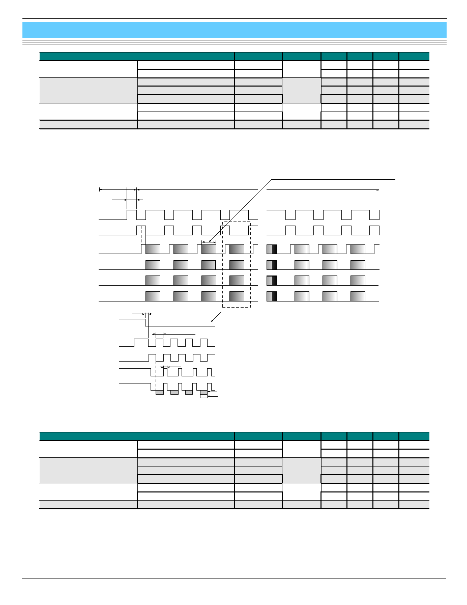
I Timing chart
G Area scanning 1 (low dark current mode)
P1V
P2V
TG
P1H
P2H, SG
RG
Vos
P1H
P2H, SG
RG
Vos
INTEGRATION PERIOD
(Shutter must be opened)
Tpwv
READOUT PERIOD
(Shutter must be closed)
1
2
3
EXPANDED VIEW
DARK SIGNAL
PHOTO GENERATED SIGNAL
D1
D2
1 HORIZONTAL-SCANNING READOUT PERIOD
P2V
TG
g
g
Tovr
Tpwh, Tpws
Tpwr
KMPDC0097EA
I Device structure, line output format
SIGNAL OUT
EXTERNAL LOAD
(2.2 k
)
∑∑∑
∑∑∑
∑∑∑
∑∑∑
∑∑∑
∑∑∑
∑∑∑
OS
OD
RD
RG
P2VS
P1VS
P2VI
P1VI
IG2V IG1V ISV
SS
TG
ISH
IG1H
IG2H
H, V: 1024
1
2
3
4
5
V
2 3 4 5
H
P1H
SG
P2H
OG
4 BLANK
4 BLANK
4 BEVEL
4 BEVEL
1024 SIGNAL OUT
1024 SIGNAL OUT
6 BEVEL
6 BEVEL
KMPDC0141EA
CCD area image sensor
S8667-1010
Parameter
Symbol
Remark
Min.
Typ.
Max.
Unit
Pulse width
Tpwv
5
-
-
µs
P1VS, P2VS, P1VI, P2VI, TG Rise and fall time
Tprv, Tpfv
*
100
-
-
ns
Pulse width
Tpwh
35
-
-
ns
Rise and fall time
Tprh, Tpfh
10
-
-
ns
P1H, P2H, SG
Duty ratio
-
*
50
-
%
Pulse width
Tpwr
15
-
-
ns
RG
Rise and fall time
Tprr, Tpfr
-
5
-
-
ns
TG (P2V) -P1H
Overlap time
Tovr
-
3
-
-
µs
*10: Symmetrical pulses should be overlapped at 50 % of maximum amplitude.
KMPDC0104EA
G Area scanning 2 (large full well mode)
P1V
P2V
TG
P1H
P2H, SG
RG
Vos
P1H
P2H, SG
RG
Vos
1
2
3
EXPANDED VIEW
Tpwr
DARK SIGNAL
PHOTO GENERATED SIGNAL
D1
D2
1 HORIZONTAL-SCANNING READOUT PERIOD
P2V
TG
Timing chart: area scanning 2 ( 7960/ 7961 eries)
INTEGRATION PERIOD
(Shutter must be opened)
Tpwv
READOUT PERIOD
(Shutter must be closed)
Tovr
Tpwh, Tpws
Parameter
Symbol
Remark
Min.
Typ.
Max.
Unit
Pulse width
Tpwv
5
-
-
µs
P1VS, P2VS, P1VI, P2VI, TG Rise and fall time
Tprv, Tpfv
*
100
-
-
ns
Pulse width
Tpwh
35
-
-
ns
Rise and fall time
Tprh, Tpfh
10
-
-
ns
P1H, P2H, SG
Duty ratio
-
*
-
50
-
%
Pulse width
Tpwr
15
-
-
ns
RG
Rise and fall time
Tprr, Tpfr
-
5
-
-
ns
TG (P2V) -P1H
Overlap time
Tovr
-
3
-
-
µs
*11: Symmetrical pulses should be overlapped at 50 % of maximum amplitude.
6

CCD area image sensor
S8667-1010
HAMAMATSU PHOTONICS K.K., Solid State Division
1126-1 Ichino-cho, Hamamatsu City, 435-8558 Japan, Telephone: (81) 053-434-3311, Fax: (81) 053-434-5184, http://www.hamamatsu.com
U.S.A.: Hamamatsu Corporation: 360 Foothill Road, P.O.Box 6910, Bridgewater, N.J. 08807-0910, U.S.A., Telephone: (1) 908-231-0960, Fax: (1) 908-231-1218
Germany: Hamamatsu Photonics Deutschland GmbH: Arzbergerstr. 10, D-82211 Herrsching am Ammersee, Germany, Telephone: (49) 08152-3750, Fax: (49) 08152-2658
France: Hamamatsu Photonics France S.A.R.L.: 8, Rue du Saule Trapu, Parc du Moulin de Massy, 91882 Massy Cedex, France, Telephone: 33-(1) 69 53 71 00, Fax: 33-(1) 69 53 71 10
United Kingdom: Hamamatsu Photonics UK Limited: 2 Howard Court, 10 Tewin Road, Welwyn Garden City, Hertfordshire AL7 1BW, United Kingdom, Telephone: (44) 1707-294888, Fax: (44) 1707-325777
North Europe: Hamamatsu Photonics Norden AB: Smidesv‰gen 12, SE-171 41 Solna, Sweden, Telephone: (46) 8-509-031-00, Fax: (46) 8-509-031-01
Italy: Hamamatsu Photonics Italia S.R.L.: Strada della Moia, 1/E, 20020 Arese, (Milano), Italy, Telephone: (39) 02-935-81-733, Fax: (39) 02-935-81-741
Information furnished by HAMAMATSU is believed to be reliable. However, no responsibility is assumed for possible inaccuracies or omissions.
Specifications are subject to change without notice. No patent rights are granted to any of the circuits described herein. ©2003 Hamamatsu Photonics K.K.
Cat. No. KMPD1058E05
Feb. 2003 DN
7
I Precaution for use (Electrostatic countermeasures)
G Handle these sensors with bare hands or wearing cotton gloves. In addition, wear anti-static clothing or use a wrist band with
an earth ring, in order to prevent electrostatic damage due to electrical charges from friction.
G Avoid directly placing these sensors on a work-desk or work-bench that may carry an electrostatic charge.
G Provide ground lines or ground connection with the work-floor, work-desk and work-bench to allow static electricity to
discharge.
G Ground the tools used to handle these sensors, such as tweezers and soldering irons.
It is not always necessary to provide all the electrostatic measures stated above. Implement these measures according to the
amount of damage that occurs.
I Element cooling/heating temperature incline rate
Element cooling/heating temperature incline rate should be set at less than 5 K/min.