
S8844-0909
S8844-0909 is an FFT-CCD area image sensor developed for measurement of low-light-level. S8844-0909 has a back-thinned structure for
detecting light from the backside that allows high sensitivity from UV to near infrared region. S8844-0909 also delivers a wide dynamic range and
low dark current when operated in MPP (Multi Pinned-Phase) mode. Spectral response characteristics are very stable making high-precision
photometry possible.
A one-stage thermoelectric cooler is built into the package along with the CCD chip. The CCD operating temperature can be maintained at -10 ∞C
when used at room temperature (25 ∞C). The CCD chip and thermoelectric cooler are hermetically sealed in the package to prevent
condensation, so no dry air is required during cooling, allowing easy handling. S8844-0909 is identical performance and pin compatible with
S7171-0909. S8844-0909 has wider FOV (Field of View) than S7171-0909 because of window structure.
Features
l Number of active pixels: 512 ◊ 512
l Greater than 90 % quantum efficiency at peak sensitivity
wavelength
l Wide spectral response range
l Low noise
l Wide dynamic range
l MPP operation
l Built-in one-stage thermoelectric cooler
Applications
l Scientific measurement
l Semiconductor inspection
l UV imaging
l Bio-photon observation
l DNA sequencer
I M A G E S E N S O R
CCD area image sensor
512 ◊ 512 pixels, Back-thinned FFT-CCD
PRELIMINARY DATA
Nov. 2002
1
I Specifications
Type No.
Cooling
Number of total pixels
Number of active
pixels
Active area
[mm (H) ◊ mm (V)]
S8844-0909
One-stage
TE-cooled
532 ◊ 520
512 ◊ 512
12.288 ◊ 12.288
I General ratings
Parameter
Specifications
Pixel size
24 (H) ◊ 24 (V) µm
Number of active pixels
512 (H) ◊ 512 (V)
Vertical clock phase
2 phase
Horizontal clock phase
2 phase
Output circuit
One-stage MOSFET source follower
Package
24 pin ceramic DIP (refer to dimensional outlines)
Built-in cooler
One-stage
Window
AR coated sapphire glass *
1
*1: Windowless type is available on custom order.

CCD area image sensor
S8844-0909
2
I Absolute maximum ratings (Ta=25 ∞C)
Parameter
Symbol
Min.
Typ.
Max.
Unit
Operating temperature
Topr
-50
-
+30
∞C
Storage temperature
Tstg
-50
-
+70
∞C
OD voltage
V
OD
-0.5
-
+25
V
RD voltage
V
RD
-0.5
-
+18
V
ISV voltage
V
ISV
-0.5
-
+18
V
ISH voltage
V
ISH
-0.5
-
+18
V
IGV voltage
V
IG1V
, V
IG2V
-10
-
+15
V
IGH voltage
V
IG1H
, V
IG2H
-10
-
+15
V
SG voltage
V
SG
-10
-
+15
V
OG voltage
V
OG
-10
-
+15
V
RG voltage
V
RG
-10
-
+15
V
TG voltage
V
TG
-10
-
+15
V
Vertical clock voltage
V
P1V
, V
P2V
-10
-
+15
V
Horizontal clock voltage
V
P1H
, V
P2H
-10
-
+15
V
I Operating conditions (MPP mode, Ta=25 ∞C)
Parameter
Symbol
Min.
Typ.
Max.
Unit
Output transistor drain voltage
V
OD
18
20
22
V
Reset drain voltage
V
RD
11.5
12
12.5
V
Output gate voltage
V
OG
1
3
5
V
Substrate voltage
V
SS
-
0
-
V
Test point (vertical input source)
V
ISV
-
V
RD
-
V
Test point (horizontal input source)
V
ISH
-
V
RD
-
V
Test point (vertical input gate)
V
IG1V
, V
IG2V
-8
0
-
V
Test point (horizontal input gate)
V
IG1H
, V
IG2H
-8
0
-
V
High
V
P1VH
, V
P2VH
4
6
8
Vertical shift register clock voltage
Low
V
P1VL
, V
P2VL
-9
-8
-7
V
High
V
P1HH
, V
P2HH
4
6
8
Horizontal shift register clock voltage
Low
V
P1HL
, V
P2HL
-9
-8
-7
V
High
V
SGH
4
6
8
Summing gate voltage
Low
V
SGL
-9
-8
-7
V
High
V
RGH
4
6
8
Reset gate voltage
Low
V
RGL
-9
-8
-7
V
High
V
TGH
4
6
8
Transfer gate voltage
Low
V
TGL
-9
-8
-7
V
I Electrical characteristics (Ta=25 ∞C)
Parameter
Symbol
Min.
Typ.
Max.
Unit
Signal output frequency
fc
-
-
1
MHz
Vertical shift register capacitance
C
P1V
, C
P2V
-
6,400
-
pF
Horizontal shift register capacitance
C
P1H
, C
P2H
-
120
-
pF
Summing gate capacitance
C
SG
-
7
-
pF
Reset gate capacitance
C
RG
-
7
-
pF
Transfer gate capacitance
C
TG
-
150
-
pF
Charge transfer efficiency *
2
CTE
0.99995
0.99999
-
-
DC output level *
3
Vout
12
15
18
V
Output impedance *
3
Zo
-
3
-
kW
Power consumption *
3
*
4
P
-
15
-
mW
*2: Charge transfer efficiency per pixel, measured at half of the full well capacity.
*3: The values depend on the load resistance. (V
OD
=20 V, Load resistance=22 kW)
*4: Power consumption of the on-chip amplifier.
CCD area image sensor
S8844-0909
3
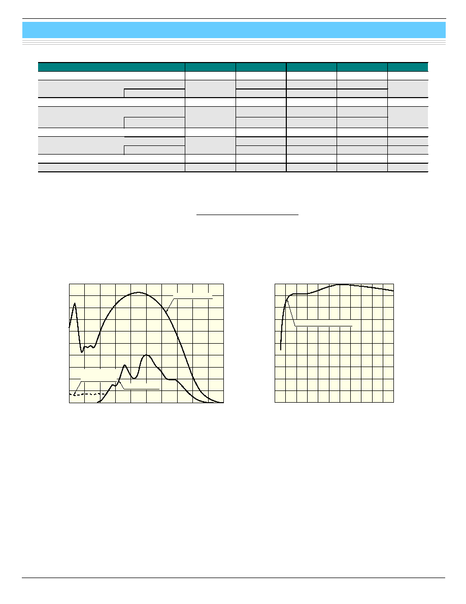
*9: Spectral response with sapphire window is decreased by
the transmittance
I Spectral response (without window)
*9
I Spectral transmittance characteristic of window material
KMPDB0058EA
QUANTUM EFFICIENCY (%)
WAVELENGTH (nm)
(Typ. Ta=25 ∞C)
0
200
400
600
800
1000
1200
10
20
30
40
50
60
70
80
90
100
FRONT-SIDED
FRONT-SIDED
(UV COAT)
BACK-THINNED
0
10
100 200
WAVELENGTH (nm)
TRANSMITTANCE (%)
300 400 500 600 700 800 900 1000 1100 1200
20
30
40
50
60
70
80
90
100
(Typ. Ta=25 ∞C)
AR COATED SAPPHIRE
KMPDB0226EA
I Electrical and optical characteristics (Ta=25 ∞C, unless otherwise noted)
Parameter
Symbol
Min.
Typ.
Max.
Unit
Saturation output voltage
Vsat
-
Fw ◊ Sv
-
V
Vertical
150,000
300,000
-
Full well capacity
Horizontal
Fw
300,000
600,000
-
e
-
CCD node sensitivity
Sv
1.8
2.2
-
µV/e
-
25 ∞C
-
4,000
12,000
Dark current *
5
(MPP mode)
0 ∞C
DS
-
200
600
e
-
/pixel/s
Readout noise *
6
Nr
-
8
16
e
-
rms
Line binning
18,750
75,000
-
-
Dynamic range *
7
Area scanning
DR
9,375
37,500
-
-
Photo response non-uniformity *
8
PRNU
-
±3
±10
%
Spectral response range
l
-
200 to 1100
-
nm
*5: Dark current nearly doubles for every 5 to 7 ∞C increase in temperature.
*6: Operating frequency is 150 kHz.
*7: Dynamic Range (DR) = Full well/Readout noise
*8: Measured at half of the full well capacity.
Photo Response Non-Uniformity (PRNU) [%] =
Signal
peak)
to
(peak
noise
pattern
Fixed
◊ 100

CCD area image sensor
S8844-0909
I Device structure
23
22
21
20
14
15
24
1
2
12
11
8
9
3
4
5
512 SIGNAL OUT
4 BLANK
4 BLANK
THINNING
THINNING
1 2 3 4
2
3
4
5
V
H
8 BEVEL
4 BEVEL
512 SIGNAL OUT
13
10
V=512
H=512
5
4 BEVEL
4 BEVEL
I Dark current vs. temperature
KMPDC0075EA
-50
-40
-30
-20
0
-10
10
20
30
TEMPERATURE (∞C)
0.1
1
10
100
1000
10000
DARK CURRENT (e
-
/pixel/s)
(Typ.)
KMPDB0037EB
4

CCD area image sensor
S8844-0909
INTEGRATION PERIOD
(Shutter must be open)
P1V
RG
OS
P2V, TG
P1H
P2H, SG
READOUT PERIOD (Shutter must be closed)
ENLARGED VIEW
4..519 520
512 + 8 (BEVEL)
Tpwv
Tovr
Tpwr
D1
D2
D3
D4
D18
D19
D20
D5..D12, S1..S512, D13..D17
P2V, TG
P1H
P2H, SG
RG
OS
Tpwh, Tpws
1
2
3
KMPDC0119EA
I Timing chart
Parameter
Symbol
Remark
Min.
Typ.
Max.
Unit
Pulse width
Tpwv
6
-
-
µs
P1V, P2V, TG
Rise and fall time
Tprv, Tpfv
*
10
200
-
-
ns
Pulse width
Tpwh
500
-
-
ns
Rise and fall time
Tprh, pfh
10
-
-
ns
P1H, P2H
Duty ratio
-
*
10
-
50
-
%
Pulse width
Tpws
500
-
-
ns
Rise and fall time
Tprs, Tpfs
10
-
-
ns
SG
Duty ratio
-
-
-
50
-
%
Pulse width
Tpwr
100
-
-
ns
RG
Rise and fall time
Tprr, Tpfr
-
5
-
-
ns
TG P1H
Overlap time
Tovr
-
3
-
-
µs
*10: Symmetrical clock pulses should be overlapped at 50 % of maximum amplitude.
5
Area scanning 1 (low dark current mode)