 | –≠–ª–µ–∫—Ç—Ä–æ–Ω–Ω—ã–π –∫–æ–º–ø–æ–Ω–µ–Ω—Ç: S9038 | –°–∫–∞—á–∞—Ç—å:  PDF PDF  ZIP ZIP |
Features
Applications
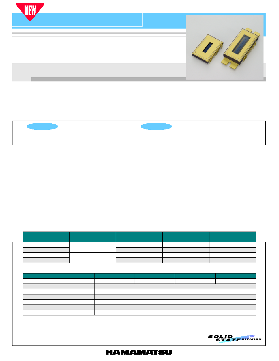
I M A G E S E N S O R
CCD image sensor
High-speed operation, back-thinned FFT-CCD
S9037/S9038 series
PRELIMINARY DATA
Oct. 2002
S9037/S9038 series FFT-CCD image sensors were developed for high-speed line scan cameras. Since an on-chip amplifier having a wide
bandwidth is used to an image sensor, a pixel rate of 10 MHz can be obtained. S9037/S9038 series image sensors also deliver a high line scan
rate equivalent to interline CCD sensors when used in line binning operation mode, because they have an active area pixel format where the
number of vertical pixels is less than the number of horizontal pixels. This makes S9037/S9038 series ideal for line scan cameras.
S9037/S9038 series image sensors have a pixel size of 24 ◊
24 µm and are available in pixel formats of 512 ◊ 4 pixels and 1024 ◊ 4 pixels.
S9038 series has a one-stage thermoelectric cooler assembled in the same package allowing stable operation at cooled temperatures. Both
S9037/S9038 series image sensors use a quartz glass window equivalent to SUPRASIL glass that provides high transmittance even at 193 nm
wavelength. These image sensors also have stable quantum efficiency in the UV region making them ideal for excimer laser monitors.
l High-speed operation: 10 MHz
l Pixel size: 24 ◊ 24 µm
l Line/pixel binning operation
l S9038 series: one-stage thermoelectric cooling
l High quantum efficiency: 90 % or more at peak
l MPP operation
l Excimer laser monitors
l High-speed line scan cameras
1
I Selection guide
Type No.
Cooling
Number of total pixels
Number of active pixels
Active area
[mm (H) ¥ mm (V)]
S9037-0902
520 ¥ 6
512 ¥ 4
12.288 ¥ 0.096
S9037-1002
Non-cooled
1044 ¥ 8
1024 ¥ 4
24.576 ¥ 0.096
S9038-0902
520 ¥ 6
512 ¥ 4
12.288 ¥ 0.096
S9038-1002
One-stage TE-cooled
1044 ¥ 8
1024 ¥ 4
24.576 ¥ 0.096
I Specifications
Parameter
S9037-0902
S9037-1002
S9038-0902
S9038-1002
Line rate
16 kHz
8 kHz
16 kHz
8 kHz
Data rate
10 MHz
Vertical clock
2 phases
Horizontal clock
2 phases
Output circuit
Two-stage MOSFET source follower
Package
24 pin metal package
Window material
Quartz window equivalent to SUPRASIL *
1
*1: Windowless type is available as option.
CCD image sensor
S9037/S9038 series
2
I Absolute maximum ratings (Ta=25 ∞C)
Parameter
Symbol
Min.
Typ.
Max.
Unit
Operating temperature
Topr
-50
-
+70
∞C
Storage temperature
Tstg
-50
-
+70
∞C
OD voltage
V
OD
-0.5
-
+25
V
RD voltage
V
RD
-0.5
-
+18
V
ISH voltage
V
ISH
-0.5
-
+18
V
IGH voltage
V
IG1H
, V
IG2H
-10
-
+15
V
SG voltage
V
SG
-10
-
+15
V
OG voltage
V
OG
-10
-
+15
V
RG voltage
V
RG
-10
-
+15
V
TG voltage
V
TG
-10
-
+15
V
Vertical clock voltage
V
P1V
, V
P2V
-10
-
+15
V
Horizontal clock voltage
V
P1H
, V
P2H
-10
-
+15
V
I Operating conditions (MPP mode, Ta=25 ∞C)
Parameter
Symbol
Min.
Typ.
Max.
Unit
Output transistor drain voltage
V
OD
12
15
-
V
Reset drain voltage
V
RD
11.5
12
12.5
V
Output gate voltage
V
OG
1
3
5
V
Substrate voltage
V
SS
-
0
-
V
Test point (horizontal input source)
V
ISH
-
V
RD
-
V
Test point (horizontal input gate)
V
IG1H
, V
IG2H
-8
0
-
V
High
V
P1VH
, V
P2VH
4
6
8
Vertical shift register
clock voltage
Low
V
P1VL
, V
P2VL
-9
-8
-7
V
High
V
P1HH
, V
P2HH
4
6
8
Horizontal shift register
clock voltage
Low
V
P1HL
, V
P2HL
-9
-8
-7
V
High
V
SGH
4
6
8
Summing gate voltage
Low
V
SGL
-9
-8
-7
V
High
V
RGH
4
6
8
Reset gate voltage
Low
V
RGL
-9
-8
-7
V
High
V
TGH
4
6
8
Transfer gate voltage
Low
V
TGL
-9
-8
-7
V
I Electrical characteristics (Ta=25 ∞C)
Parameter
Symbol
Remark
Min.
Typ.
Max.
Unit
Signal output frequency
fc
-
-
-
10
MHz
Reset clock frequency
frg
-
-
-
10
MHz
-0902
-
-
300
-
pF
Vertical shift register capacitance
-1002
C
P1V
, C
P2V
-
-
500
-
pF
-0902
-
-
200
-
pF
Horizontal shift register capacitance
-1002
C
P1H
, C
P2H
-
-
300
-
pF
Summing gate capacitance
C
SG
-
-
7
-
pF
Reset gate capacitance
C
RG
-
-
7
-
pF
Transfer gate capacitance
C
TG
-
-
15
-
pF
Transfer efficiency
CTE
*
2
-
0.99995
-
-
DC output level
Vout
-
-
7
-
V
Output impedance
Zo
*
3
-
500
-
9
Power dissipation
P
*
3,
*
4
-
100
-
mW
*2: Charge transfer efficiency per pixel, measured at half of the full well capacity.
*3: This depends on the output transistor drain voltage.
*4: Power dissipation of the on-chip amplifier.
CCD image sensor
S9037/S9038 series
I Electrical and optical characteristics (Ta=25
∞
C, unless otherwise noted)
Parameter
Symbol
Min.
Typ.
Max.
Unit
Saturation output voltage
Vsat
Fw ¥ Sv
V
Vertical
-
300
-
Full well capacity
Horizontal (summing)
Fw
-
600
-
ke
-
CCD node sensitivity
Sv
-
1.2
-
µV/e
-
25 ∞C
-
4,000
-
Dark current *
5
(MPP mode)
0 ∞C
DS
-
200
-
e
-
/pixel/s
Readout noise *
6
Nr
-
100
-
e
-
rms
Dynamic range (line binning)
DR
-
6000
-
-
Photo response non-uniformity *
7
PRNU
-
-
±10
%
Spectral response range (without window)
l
-
200 to 1100
-
nm
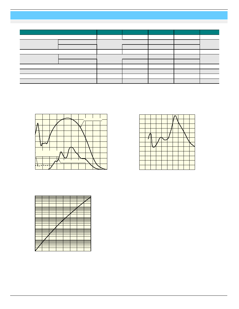
*5: Dark current nearly doubles for every 5 to 7 ∞C increase in temperature.
*6: -40 ∞C, operating frequency is 80 kHz.
*7: Condition: half of saturation output voltage.
QUANTUM EFFICIENCY (%)
WAVELENGTH (nm)
(Typ. Ta=25 ∞C)
0
200
400
600
800
1000
1200
10
20
30
40
50
60
70
80
90
100
FRONT-ILLUMINATED
FRONT-ILLUMINATED
(UV COAT)
BACK-THINNED
I Spectral response
I Spectral response of photosensitive surface
(without cap)
KMPDB0150EA
KMPDB0058EA
I Dark current vs. temperature
-50
-40
-30
-20
0
-10
10
20
30
TEMPERATURE (∞C)
0.1
1
10
100
1000
10000
DARK CURRENT (e
-
/pixel/s)
(Typ.)
KMPDB0037EB
3
WAVELENGTH (nm)
(Typ. Ta=25 ∞C)
QUANTUM EFFICIENCY (%)
120
100
0
20
40
120
100
80
60
140
160
180
200
CCD image sensor
S9037/S9038 series
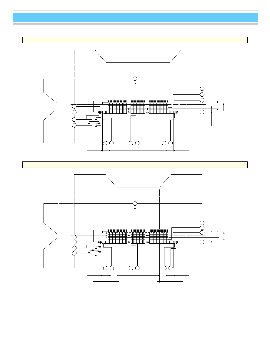
I Device structure
S9037/S9038-0902
1
THINNING
THINNING
SS
RG
RD
OD
OS
OG
4 BLANK
SG
P2H
P1H
4 BLANK
512 ACTIVE
2 BEVEL
IG2H
IG1H
ISH
TG
P2V
P1V
4 ACTIVE
6
KMPDC0159EC
S9037/S9038-1002
1
THINNING
THINNING
SS
RD
OD
OS
OG
4 BLANK
SG
P2H
P1H
6 BEVEL
6 BEVEL
4 BLANK
1024 ACTIVE
3 BEVEL
1 BEVEL
4 ACTIVE
IG2H
IG1H
P2V
P1V
8
RG
ISH
TG
KMPDC0160EB
4
CCD image sensor
S9037/S9038 series
KMPDC0161E¡
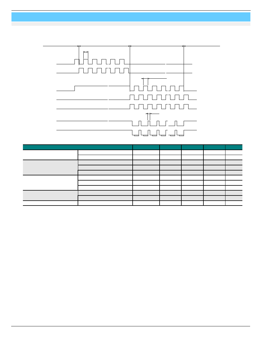
I Timing chart (line binning)
Parameter
Symbol
Min.
Typ.
Max.
Unit
Pulse width
Tpwv
1
-
-
µs
P1V, P2V, TG
Rise and fall time
Tprv, Tpfv
-
20
-
ns
Pulse width
Tpwh
50
-
-
ns
Rise and fall time
Tprh, Tpfh
-
10
-
ns
P1H, P2H
Duty ratio
-
-
50
-
%
Pulse width
Tpws
50
-
-
ns
Rise and fall time
Tprs, Tpfs
-
10
-
ns
SG
Duty ratio
-
-
50
-
%
Pulse width
Tpwr
-
15
-
ns
RG
Rise and fall time
Tprr, Tpfr
5
-
-
ns
TG (P2V) - P1H
Overlap time
Tovr
3
-
-
µs
Tpwv
Tpwh, Tpws
P1V
P2V, TG
P1H
P2H
SG
RG
Vos
Tpwr
VERTICAL BINNING PERIOD
INTEGRATION PERIOD
INTEGRATION PERIOD
READOUT PERIOD
5
CCD image sensor
S9037/S9038 series
WINDOW 16.3
8.2
34.0
2.54
22.9
22.4
0.096
ACTIVE AREA
12.29
4.4
4.8
2.4
3.8
PHOTOSENSITIVE SURFACE
INDEX MARK
PIN No. 1
3.0
(24 ◊) 0.5
WINDOW 28.6
22.9
22.4
ACTIVE AREA 24.58
0.096
8.2
44.0
2.54
3.0
PHOTOSENSITIVE SURFACE
4.4
2.4
4.8
3.8
INDEX MARK
PIN No. 1
(24 ◊) 0.5
WINDOW 16.3
8.2
34.0
50.0
2.54
22.9
19.0
4.0
42.0
22.4
0.096
7.3
1.0
7.7
6.7
4.8
ACTIVE AREA
12.29
PHOTOSENSITIVE SURFACE
INDEX MARK
PIN No. 1
3.0
TE-COOLER
(24 ◊) 0.5
KMPDA0156EA
KMPDA0155EA
I Dimensional outlines (unit: mm)
KMPDA0153EB
KMPDA0154EA
(24 ◊) 0.5
7.3
1.0
3.0
6.7
4.8
PHOTOSENSITIVE SURFACE
7.7
INDEX MARK
PIN No. 1
0.096
4.0
19.0
22.4
22.9
44.0
52.0
60.0
2.54
WINDOW 28.6
ACTIVE AREA 24.58
8.2
TE-COOLER
S9037-1002
S9038-0902
S9038-1002
S9037-0902
6

CCD image sensor
S9037/S9038 series
7
WINDOW 16.3
4.5
34.0
2.54
22.9
22.4
0.096
ACTIVE AREA
12.29
4.8
2.4
PHOTOSENSITIVE SURFACE
INDEX MARK
PIN No. 1
3.0
(24 ◊) 0.5
WINDOW 28.6
22.9
22.4
ACTIVE AREA 24.58
0.096
4.5
44.0
2.54
3.0
PHOTOSENSITIVE SURFACE
2.4
4.8
INDEX MARK
PIN No. 1
(24 ◊) 0.5
WINDOW 16.3
4.5
34.0
50.0
2.54
22.9
19.0
4.0
42.0
22.4
0.096
1.0
7.7
4.8
ACTIVE AREA
12.29
PHOTOSENSITIVE SURFACE
INDEX MARK
PIN No. 1
3.0
TE-COOLER
(24 ◊) 0.5
KMPDA0168EA
KMPDA0167EA
I Dimensional outlines of windowless types (unit: mm)
KMPDA0165EA
KMPDA0166EA
(24 ◊) 0.5
1.0
3.0
4.8
PHOTOSENSITIVE SURFACE
7.7
INDEX MARK
PIN No. 1
0.096
4.0
19.0
22.4
22.9
44.0
52.0
60.0
2.54
WINDOW 28.6
ACTIVE AREA 24.58
4.5
TE-COOLER
S9037-1002N
S9038-0902N
S9038-1002N
S9037-0902N
I P in c o n n e c tio n s
S 9 0 3 7 s e rie s
S 9 0 3 8 s e rie s
P in
N o .
S y m b o l
D e s c rip tio n
R e m a rk
S y m b o l
D e s c rip tio n
R e m a rk
1
R D
R e s e t d ra in
+ 1 2 V R D
R e s e t d ra in
+ 1 2 V
2
O S
O u tp u t tra n s is to r s o u rc e
External R
2
=2.2 k9
O S
O u tp u t tra n s is to r s o u rc e
External R
L
=2.2 k9
3
O D
O u tp u t tra n s is to r d ra in
+ 1 5 V
O D
O u tp u t tra n s is to r d ra in
+ 1 5 V
4
O G
O u tp u t g a te
+ 3 V
O G
O u tp u t g a te
+ 3 V
5
S G
S u m m in g g a te
Same timing as
P2H
S G
S u m m in g g a te
Same timing as
P2H
6
-
-
7
-
-
8
P 2 H
C C D h o riz o n ta l re g is te r c lo c k -2
P 2 H
C C D h o riz o n ta l re g is te r c lo c k -2
9
P 1 H
C C D h o riz o n ta l re g is te r c lo c k -1
P 1 H
C C D h o riz o n ta l re g is te r c lo c k -1
1 0
IG 2 H
T e s t p o in t (h o rizo n ta l in p u t
g a te -2 )
G N D
IG 2 H
T e s t p o in t (h o rizo n ta l in p u t
g a te -2 )
G N D
1 1
IG 1 H
T e s t p o in t (h o rizo n ta l in p u t
g a te -1 )
G N D
IG 1 H
T e s t p o in t (h o rizo n ta l in p u t
g a te -1 )
G N D
1 2
IS H
T e s t p o in t (h o rizo n ta l in p u t
s o u rc e )
S h o rte d to R D
IS H
T e s t p o in t (h o rizo n ta l in p u t
s o u rc e )
S h o rte d to R D
1 3
T G
T ra n s fe r g a te
Same timing as
P2V
T G
T ra n s fe r g a te
Same timing as
P2V
1 4
P 2 V
C C D v e rtic a l re g is te r c lo c k -2
P 2 V
C C D v e rtic a l re g is te r c lo c k -2
1 5
P 1 V
C C D v e rtic a l re g is te r c lo c k -1
P 1 V
C C D v e rtic a l re g is te r c lo c k -1
1 6
N C
T h 1
T h e rm is to r
1 7
N C
T h 2
T h e rm is to r
1 8
N C
P -
T E -c o o le r-
1 9
N C
P +
T E -c o o le r+
2 0
S S
S u b s tra te (G N D )
G N D
S S
S u b s tra te (G N D )
2 1
N C
N C
2 2
N C
N C
2 3
N C
N C
2 4
R G
R e s e t g a te
R G
R e s e t g a te

CCD image sensor
S9037/S9038 series
I Specifications of built-in TE-cooler (Typ.)
Parameter
Symbol
Condition
S9038-0902
S9038-1002
Unit
Internal resistance
Rint
Ta=25 ∞C
2.5
1.2
9
Maximum current *
&
Imax Tc *
'
=Th *
=25 ∞C
1.5
3.0
A
Maximum voltage
Vmax Tc *
'
=Th *
=25 ∞C
3.8
3.6
V
Maximum heat absorption*
Qmax
3.4
5.1
W
Maximum temperature
of heat radiating side
-
70
70
∞
C
*8: Maximum current Imax:
If the current greater than this value flows into the thermoelectric cooler, the heat absorption begins to decrease due to the
Joule heat. It should be noted that this value is not the damage threshold value. To protect the thermoelectric cooler and
maintain stable operation, the supply current should be less than 60 % of this maximum current.
*9: Temperature of the cooling side of thermoelectric cooler.
*10: Temperature of the heat radiating side of thermoelectric cooler.
*11: Maximum heat absorption Qmax.
This is a theoretical heat absorption level that offsets the temperature difference in the thermoelectric cooler when the
maximum current is supplied to the unit.
0
1
2
3
V
O
L
T
A
GE (V)
CCD TEMPERA
TURE
(
∞
C)
4
7
6
5
-40
-30
4
3
2
CURRENT (A)
1
0
-20
-10
0
10
20
30
(Typ. Ta=25 ∞C)
VOLTAGE vs. CURRENT
CCD TEMPERATURE vs. CURRENT
0
1
2
3
V
O
L
T
A
GE (V)
CCD TEMPERA
TURE
(
∞
C)
4
7
6
5
-40
-30
2.0
1.5
1.0
CURRENT (A)
0.5
0
-20
-10
0
10
20
30
(Typ. Ta=25 ∞C)
VOLTAGE vs. CURRENT
CCD TEMPERATURE vs. CURRENT
KMPDB0178EA
KMPDB0179EA
S9038-0902
S9038-1002
I Specifications of built-in temperature sensor
A chip thermistor is built in the same package with a CCD chip, and the CCD chip temperature can be monitored with it. A relation
between the thermistor resistance and absolute temperature is expressed by the following equation.
R1 = R2 ◊ expB (1 / T1 - 1 / T2)
where R1 is the resistance at absolute temperature T1 (K)
R2 is the resistance at absolute temperature T2 (K)
B is so-called the B constant (K)
The characteristics of the thermistor used are as follows.
R (298K) = 10 kW
B (298K / 323K) = 3450 K
KMPDB0111EA
(Typ. Ta=25 ∞C)
10 k
220
240
260
TEMPERATURE (K)
RESIST
ANCE
280
300
100 k
1 M
8

HAMAMATSU PHOTONICS K.K., Solid State Division
1126-1 Ichino-cho, Hamamatsu City, 435-8558 Japan, Telephone: (81) 053-434-3311, Fax: (81) 053-434-5184, http://www.hamamatsu.com
U.S.A.: Hamamatsu Corporation: 360 Foothill Road, P.O.Box 6910, Bridgewater, N.J. 08807-0910, U.S.A., Telephone: (1) 908-231-0960, Fax: (1) 908-231-1218
Germany: Hamamatsu Photonics Deutschland GmbH: Arzbergerstr. 10, D-82211 Herrsching am Ammersee, Germany, Telephone: (49) 08152-3750, Fax: (49) 08152-2658
France: Hamamatsu Photonics France S.A.R.L.: 8, Rue du Saule Trapu, Parc du Moulin de Massy, 91882 Massy Cedex, France, Telephone: 33-(1) 69 53 71 00, Fax: 33-(1) 69 53 71 10
United Kingdom: Hamamatsu Photonics UK Limited: 2 Howard Court, 10 Tewin Road, Welwyn Garden City, Hertfordshire AL7 1BW, United Kingdom, Telephone: (44) 1707-294888, Fax: (44) 1707-325777
North Europe: Hamamatsu Photonics Norden AB: Smidesv‰gen 12, SE-171 41 Solna, Sweden, Telephone: (46) 8-509-031-00, Fax: (46) 8-509-031-01
Italy: Hamamatsu Photonics Italia S.R.L.: Strada della Moia, 1/E, 20020 Arese, (Milano), Italy, Telephone: (39) 02-935-81-733, Fax: (39) 02-935-81-741
Information furnished by HAMAMATSU is believed to be reliable. However, no responsibility is assumed for possible inaccuracies or omissions.
Specifications are subject to change without notice. No patent rights are granted to any of the circuits described herein. ©200
3 Hamamatsu Photonics K.K.
Cat. No. KMPD1067E03
Feb. 2003 DN
CCD image sensor
S9037/S9038 series
I Precaution for use (Electrostatic countermeasures)
G Handle these sensors with bare hands or wearing cotton gloves. In addition, wear anti-static clothing and use a wrist band
with an earth ring, in order to prevent electrostatic damage due to electrical charges from friction.
G Avoid directly placing these sensors on a work-desk or work-bench that may carry an electrostatic charge.
G Provide ground lines or ground connection with the work-floor, work-desk and work-bench to allow static electricity to
discharge.
G Ground the tools used to handle these sensors, such as tweezers and soldering irons.
It is not always necessary to provide all the electrostatic measures stated above. Implement these measures according to the
amount of damage that occurs.
I Element cooling/heating temperature incline rate
Element cooling/heating temperature incline rate should be set at less than 5 K/min.
9