S9049
Features
Applications
P H O T O D I O D E
Si photodiode
l Higher moisture resistance than conventional products
l Visible filter of organic material
l Active area: 2 ◊ 2 mm
l SIP (Single Inline Package)
l High sensitivity, low dark current
l Wide storage temperature range
l Illuminance measurement
l Light level control
l Display brightness control, etc.
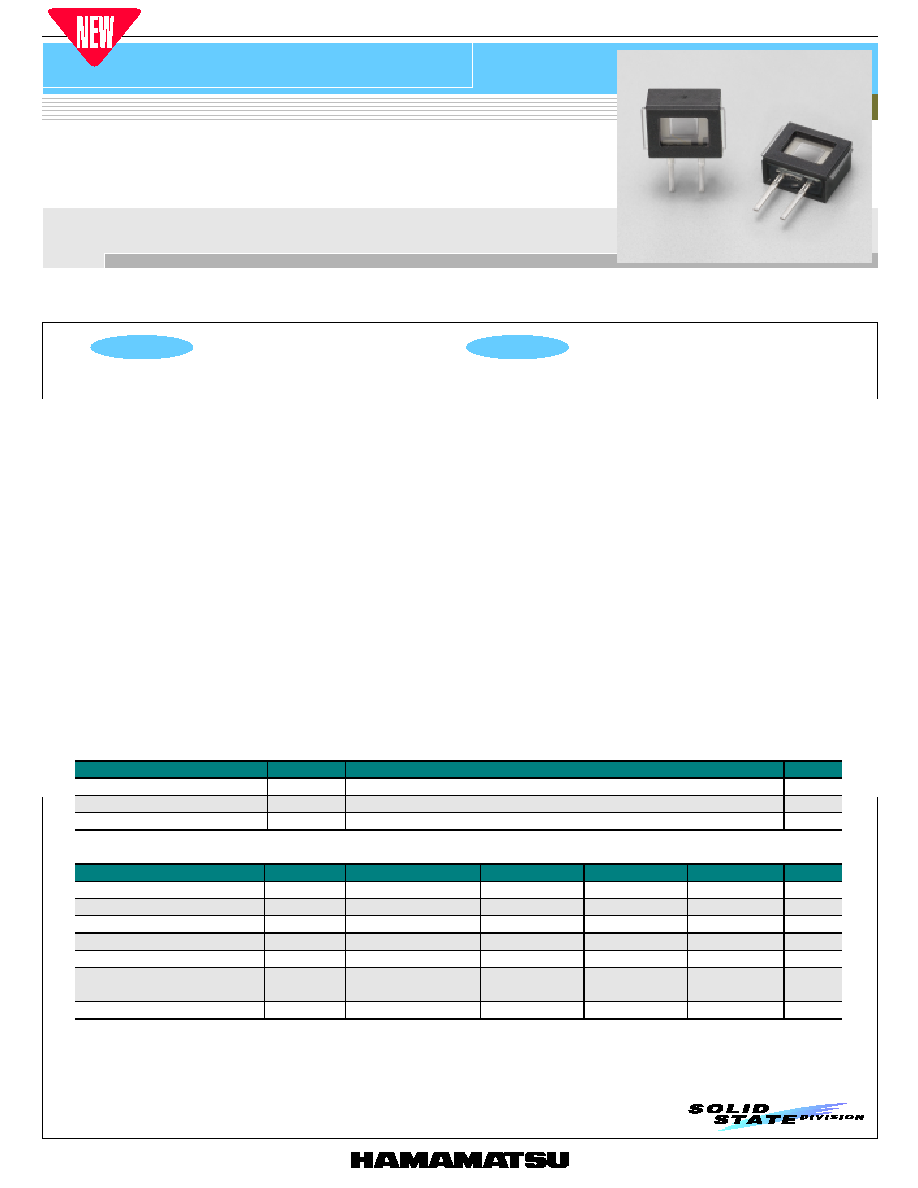
Photodiode with moisture-resistant filter
S9049 is a Si photodiode designed for visible light detection and molded into a SIP (Single Inline Package) with a visible-compensation filter
made from organic material. This organic filter significantly reduces a loss of light transmittance which is a shortcoming of inorganic visible-
compensation filter.
1
1
I Absolute maximum ratings
Parameter
Symbol
Value
Unit
Reverse voltage
V
R
Max.
10
V
Operating temperature
Topr
-25 to +85
∞C
Storage temperature
Tstg
-40 to +100
∞C
I Electrical and optical characteristics (Ta=25 ∞C)
Parameter
Symbol
Condition
Min.
Typ.
Max.
Unit
Spectral response range
l
-
420 to 700
-
nm
Peak sensitivity wavelength
lp
-
660
-
nm
Photo sensitivity
S
l=lp
-
0.33
-
A/W
Short circuit current
Isc
100 lx, 2856 K
400
500
-
nA
Dark current
I
D
V
R
=1 V
-
-
10
pA
Rise time
tr
V
R
=0 V, R
L
=1 kW
10 to 90 %
-
2
-
µs
Terminal capacitance
Ct
V
R
=0 V, f=10 kHz
-
0.5-
nF

Si photodiode
S9049
2
HAMAMATSU PHOTONICS K.K., Solid State Division
1126-1 Ichino-cho, Hamamatsu City, 435-8558 Japan, Telephone: (81) 053-434-3311, Fax: (81) 053-434-5184, http://www.hamamatsu.com
U.S.A.: Hamamatsu Corporation: 360 Foothill Road, P.O.Box 6910, Bridgewater, N.J. 08807-0910, U.S.A., Telephone: (1) 908-231-0960, Fax: (1) 908-231-1218
Germany: Hamamatsu Photonics Deutschland GmbH: Arzbergerstr. 10, D-82211 Herrsching am Ammersee, Germany, Telephone: (49) 08152-3750, Fax: (49) 08152-2658
France: Hamamatsu Photonics France S.A.R.L.: 8, Rue du Saule Trapu, Parc du Moulin de Massy, 91882 Massy Cedex, France, Telephone: 33-(1) 69 53 71 00, Fax: 33-(1) 69 53 71 10
United Kingdom: Hamamatsu Photonics UK Limited: 2 Howard Court, 10 Tewin Road, Welwyn Garden City, Hertfordshire AL7 1BW, United Kingdom, Telephone: (44) 1707-294888, Fax: (44) 1707-325777
North Europe: Hamamatsu Photonics Norden AB: Smidesv‰gen 12, SE-171 41 Solna, Sweden, Telephone: (46) 8-509-031-00, Fax: (46) 8-509-031-01
Italy: Hamamatsu Photonics Italia S.R.L.: Strada della Moia, 1/E, 20020 Arese, (Milano), Italy, Telephone: (39) 02-935-81-733, Fax: (39) 02-935-81-741
Information furnished by HAMAMATSU is believed to be reliable. However, no responsibility is assumed for possible inaccuracies or omissions.
Specifications are subject to change without notice. No patent rights are granted to any of the circuits described herein. ©2003 Hamamatsu Photonics K.K.
Cat. No. KSPD1060E02
Jan. 2003 DN
2
200
400
600
800
1000
1200
WAVELENGTH (nm)
0
0.1
0.2
0.3
0.4
0.5
PHOTO SENSITIVITY (A/W)
(Typ. Ta=25 ∞C)
QE=100 %
1.0
1.0
(0.4)
4.0
6.0 *
(0.4)
(2.4)
(0.27)
3.0
0.25
0.8
3.0
1.2
(2 ◊) 0.5
(2 ◊) 0.4
2.54
1.2
0.25
1.5
Tolerance unless otherwise noted: ±0.2, ±2∞
Shaded area indicates burr.
Chip position accuracy with respect to the
package dimensions marked *
X, Y
±0.4, ±4∞
ACTIVE AREA
2.0 ◊ 2.0
(4.43)
5.0 *
(0.95)
(0.8)
(4.6)
PHOTOSENSITIVE
SURFACE
(0.33)
I Spectral response
I Dark current vs. reverse voltage
I Dimensional outline
REVERSE VOLTAGE (V)
DARK CURRENT
0.01
0.1
10
1
100
10 fA
100 fA
1 pA
10 pA
1 µA
100 nA
10 nA
1 nA
100 pA
(Typ. Ta=25 ∞C)
KSPDB0222EA
KSPDB0220EA
KSPDA0155EA