Features
l Sensor for acquiring 2D projection data
l High-speed frame rate
l Low power consumption
l 10-bit/8-bit switchable ADC
Applications
l Light spot position detection (printers, FA inspection
equipment, amusement machines)
l Moving object detection (FA inspection equipment,
amusement machines)
l 3D measurement (FA inspection equipment,
medical measurement)
I M A G E S E N S O R
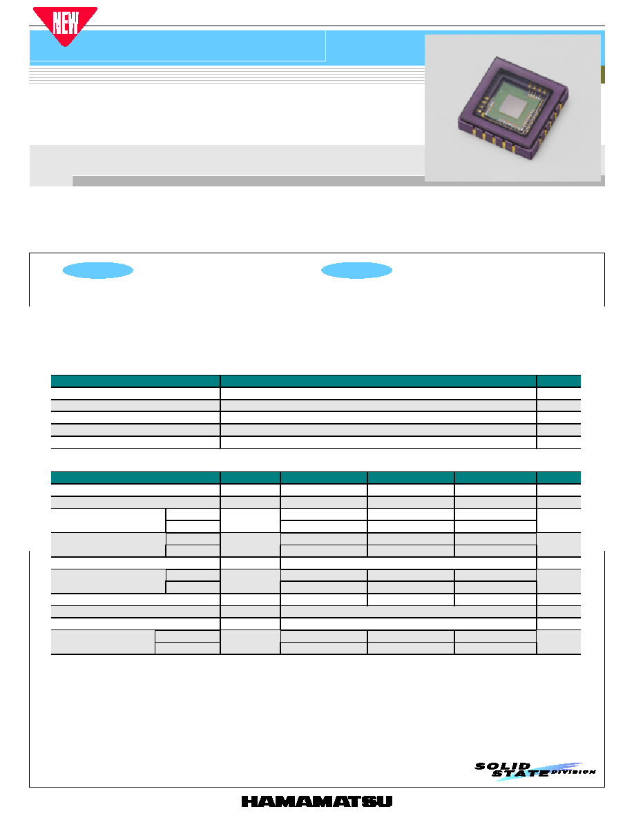
Profile sensor
High-speed sensor capable of acquiring two-dimensional projection data
S9132
The profile sensor S9132 is a high-performance CMOS area image sensor particularly intended to acquire projection data. S9132 is designed
specifically as an area image sensor for acquiring a projection profile in the X and Y directions, and therefore allows high-speed position detection
and moving object detection even from very small amounts of information compared to normal area image sensors. S9132 also has advantages
over convensional 2D PSDs (Position Sensitive Detectors) that the output linearity is improved, multiple light spots can be detected and external
circuits are simplified. A timing generator, bias voltage generator and 10-bit AD converter circuits are all integrated on the same chip, allowing
operations with a very simple external driver circuit and external signal processing circuit.
1
I Shape specifications
Parameter
Specification
Unit
Number of pixels
256 � 256
-
Pixel pitch
7.8
�m
Active area
1.9968 � 1.9968
mm
Package
20-pin LCC package
-
Package size
7.6 � 7.6
mm
I Electrical and optical characteristics [Ta=25 �C, Vdd=5 V, V (CLK)=V (ST)=5 V]
Parameter
Symbol
Min.
Typ.
Max.
Unit
Analog supply voltage
Vdd (A)
4.75
5
5.25
V
Digital supply voltage
Vdd (D)
4.75
5
Vdd (A)
V
High gain
-
100
300
Dark output voltage *
Low gain
Vd
-
20
60
mV
High gain
3
3.5
-
Saturation output voltage
Low gain
Vsat
2.5
3
-
V
Spectral response range
l
350 to 1150
nm
High gain
-
40
-
Photo sensitivity *
Low gain
RES
-
8
-
V/nJ
Photo response non-uniformity *
!
PRNU
-
-
�10
%
Digital video output form
-
Serial output
Resolution
RESO
10 or 8
bit
10-bit mode
2.4
-
-
Conversion time
8-bit mode
tCON
1.2
-
-
�s/ch
*1: Storage time Ts=100 ms
*2: l=780 nm
*3: Photo response non-uniformity is non-uniformity in the output from 236 pixels (first and last 10 pixels are excluded) in the X or
Y direction, measured when the sensor is illuminated with white uniform light at an intensity level of 50 % of the saturation.
PRNU=DV/V � 100 (%)
V: the average output of all pixels, DV: the difference from the maximum or minimum output and V

Profile sensor
S9132
HAMAMATSU PHOTONICS K.K., Solid State Division
1126-1 Ichino-cho, Hamamatsu City, 435-8558 Japan, Telephone: (81) 053-434-3311, Fax: (81) 053-434-5184, http://www.hamamatsu.com
U.S.A.: Hamamatsu Corporation: 360 Foothill Road, P.O.Box 6910, Bridgewater, N.J. 08807-0910, U.S.A., Telephone: (1) 908-231-0960, Fax: (1) 908-231-1218
Germany: Hamamatsu Photonics Deutschland GmbH: Arzbergerstr. 10, D-82211 Herrsching am Ammersee, Germany, Telephone: (49) 08152-3750, Fax: (49) 08152-2658
France: Hamamatsu Photonics France S.A.R.L.: 8, Rue du Saule Trapu, Parc du Moulin de Massy, 91882 Massy Cedex, France, Telephone: 33-(1) 69 53 71 00, Fax: 33-(1) 69 53 71 10
United Kingdom: Hamamatsu Photonics UK Limited: 2 Howard Court, 10 Tewin Road, Welwyn Garden City, Hertfordshire AL7 1BW, United Kingdom, Telephone: (44) 1707-294888, Fax: (44) 1707-325777
North Europe: Hamamatsu Photonics Norden AB: Smidesv�gen 12, SE-171 41 Solna, Sweden, Telephone: (46) 8-509-031-00, Fax: (46) 8-509-031-01
Italy: Hamamatsu Photonics Italia S.R.L.: Strada della Moia, 1/E, 20020 Arese, (Milano), Italy, Telephone: (39) 02-935-81-733, Fax: (39) 02-935-81-741
Information furnished by HAMAMATSU is believed to be reliable. However, no responsibility is assumed for possible inaccuracies or omissions.
Specifications are subject to change without notice. No patent rights are granted to any of the circuits described herein. �2003 Hamamatsu Photonics K.K.
Cat. No. KMPD1075E02
Jan. 2003 DN
2
I Dimensional outline (unit: mm)
KMPDA0174EA
I Conceptual view of light spot detection
KMPDC0168EA
LIGHT SPOT
X-DIRECTION PROJECTION DATA
Y
-DIRECTION PR
OJECTION D
A
T
A
1.00 � 0.15
11
15
5
1
16
20
10
6
11
0.508 � 0.08
1.016
20
16
10
ACTIVE AREA 2.00
o7.20 � 0.1
o7.60 � 0.2
1.016 � 0.08
1.77
1.48
0.55 � 0.05
1.10 � 0.2
1.40 � 0.14
1
5
6
15
4.06 � 0.13
ACTIVE AREA
INDEX MARK
Pin No.
Symbol
I/O
Function
1
Vsel (X)
I
AD mode selection voltage
2
Vg (X)
I
Gain selection voltage
3
ST (X)
I
Start pulse
4
CLK (X)
I
Clock pulse
5
EOS (X)
O
End of scan pulse
6
CLK (Y)
I
Clock pulse
7
ST (Y)
I
Start pulse
8
Vdd (A)
I
Analog supply voltage
9
Vg (Y)
I
Gain selection voltage
10
Vsel (Y)
I
AD mode selection voltage
11
Vss (A)
I
Analog ground
12
Vss (D)
I
Digital ground
13
Trig (Y)
O
Trigger pulse
14
DO (Y)
O
Digital output
15
Vdd (D)
I
Digital supply voltage
16
NC
No connection
17
DO (X)
O
Digital output
18
Trig (X)
O
Trigger pulse
19
EOC (X)
O
End of conversion pulse
20
Vss (A)
I
Analog ground
I Pin connection