 | –≠–ª–µ–∫—Ç—Ä–æ–Ω–Ω—ã–π –∫–æ–º–ø–æ–Ω–µ–Ω—Ç: S9227 | –°–∫–∞—á–∞—Ç—å:  PDF PDF  ZIP ZIP |
S9227
Features
l Pixel pitch: 12.5 µm
Pixel height: 250 µm
l Number of pixels: 512 ch
l Single 5 V power supply operation
l Video data rate: 5 MHz Max.
l Simultaneous charge integration
l Shutter function
l High sensitivity, low dark current, low noise
l Built-in timing generator allows operation with only
start and clock pulse inputs
l Spectral response range: 400 to 1000 nm
l 8-pin DIP, 16-pin surface mount type also available
Applications
l Position detection
l Image reading
I M A G E S E N S O R
CMOS linear image sensor
High-speed readout, simultaneous integration
S9227 is a small CMOS linear image sensor designed for image input applications. Signal charge is integrated on all pixels simultaneously and
then read out at high speeds of 5 MHz.
PRELIMINARY DATA
Jan. 2003
1
I Absolute maximum ratings
Parameter
Symbol
Value
Unit
Supply voltage
Vdd
-0.3 to +6
V
Clock pulse voltage
V (CLK)
-0.3 to +6
V
Start pulse voltage
V (ST)
-0.3 to +6
V
Operating temperature *
1
Topr
-5 to +60
∞C
Storage temperature
Tstg
-10 to +70
∞C
*1: No condensation
I Mechanical specifications
Parameter
Value
Unit
Number of pixels
512
-
Pixel pitch
12.5
µm
Pixel height
250
µm
Active area length
6.4
mm
Window material
TEMPAX
-
CMOS linear image sensor
S9227
2
I Recommended terminal voltage
Parameter
Symbol
Min.
Typ.
Max.
Unit
Supply voltage
Vdd
4.75
5
5.25
V
High
Vdd-0.25
Vdd
Vdd+0.25
V
Clock pulse voltage
Low
V (CLK)
-
0
-
V
High
Vdd-0.25
Vdd
Vdd+0.25
V
Start pulse voltage
Low
V (ST)
-
0
-
V
I Electrical characteristics [Ta=25 ∞C, Vdd=5 V, V (CLK) =V (ST)=5 V]
Parameter
Symbol
Min.
Typ.
Max.
Unit
Clock pulse frequency
f (CLK)
0.001
-
5
MHz
Video data rate
VR
-
f (CLK)
-
MHz
Power consumption
P
-
150
-
mW
Conversion efficiency
CE
-
1.6
-
µV/e
-
I Electrical and optical characteristics [Ta=25 ∞C, Vdd=5 V, V (CLK)=V (ST)=5 V]
Parameter
Symbol
Min.
Typ.
Max.
Unit
Spectral response range
l
400 to 1000
nm
Peak sensitivity wavelength
lp
-
700
-
nm
Dark current
I
,
-
5
-
fA
Saturation charge
Qsat
-
420
-
fC
Dark output voltage *
2
Vd
-
0.5
5
mV
Saturation output voltage
Vsat
-
4.2
-
V
Readout noise
Nr
-
0.4
-
mV-rms
Offset output voltage
Vo
-
0.6
-
V
Photo response non-uniformity *
3
*
4
PRNU
-
-
±5
%
*2: Storage time Ts=10 ms
*3: Uniformity is defined under the condition that the device is uniformly illuminated by light which is 50 % of the saturation
exposure level as follows:
PRNU= DX/X ◊ 100 (%)
Where X is the average output of all pixels and DX is the difference from the maximum or minimum output and X.
*4: Measured with a tungsten lamp of 2856 K.
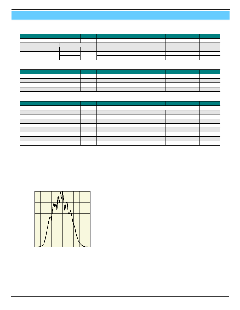
I Spectral response (typical example)
KMPDB0230EA
80
200
600
1000
300 400
800
700
1100
500
900
1200
WAVELENGTH (nm)
RELATIVE SENSITIVITY (%)
0
60
100
40
20
(Typ. Ta=25 ∞C)
CMOS linear image sensor
S9227
I Timing chart
KMPDC0166EA
3
Parameter
Symbol
Min.
Typ.
Max.
Unit
Start pulse width
tpw (ST)
T1 ◊ 530
-
-
ns
Start pulse high width
thw (ST)
T1 ◊ 3
-
-
ns
Start pulse low width
tlw (ST)
T1 ◊ 15
-
-
ns
Start pulse rise and fall time
tr (ST), tf (ST)
0
20
30
ns
Clock pulse width
tpw (CLK), T1
200
-
-
ns
Clock pulse rise and fall time
tr (CLK), tf (CLK)
0
20
30
ns
Video delay time 1
tvd1
-
30
-
ns
Video delay time 2
tvd2
-
40
-
ns
Note) The internal circuit starts operating at the rise of CLK pulse immediately after ST pulse sets to low.
The integration time equals the high period of ST pulse plus 6 CLK cycles.
tpw (CLK), T1
tlw (ST)
2.5 CLOCKS
8.5 CLOCKS
INTEGRATION TIME
1 2 3 4
13
CLK
SP
Video
EOS
CLK
SP
CLK
Video
1415
thw (ST)
15 CLOCKS
tf (CLK)
tf (ST)
tr (ST)
tr (CLK)
tvd2
tvd1
tlw (ST)
thw (ST)
tpw (ST)
tpw (CLK)
tpw (ST)
512
Trig
CMOS linear image sensor
S9227
HAMAMATSU PHOTONICS K.K., Solid State Division
1126-1 Ichino-cho, Hamamatsu City, 435-8558 Japan, Telephone: (81) 053-434-3311, Fax: (81) 053-434-5184, http://www.hamamatsu.com
U.S.A.: Hamamatsu Corporation: 360 Foothill Road, P.O.Box 6910, Bridgewater, N.J. 08807-0910, U.S.A., Telephone: (1) 908-231-0960, Fax: (1) 908-231-1218
Germany: Hamamatsu Photonics Deutschland GmbH: Arzbergerstr. 10, D-82211 Herrsching am Ammersee, Germany, Telephone: (49) 08152-3750, Fax: (49) 08152-2658
France: Hamamatsu Photonics France S.A.R.L.: 8, Rue du Saule Trapu, Parc du Moulin de Massy, 91882 Massy Cedex, France, Telephone: 33-(1) 69 53 71 00, Fax: 33-(1) 69 53 71 10
United Kingdom: Hamamatsu Photonics UK Limited: 2 Howard Court, 10 Tewin Road, Welwyn Garden City, Hertfordshire AL7 1BW, United Kingdom, Telephone: (44) 1707-294888, Fax: (44) 1707-325777
North Europe: Hamamatsu Photonics Norden AB: Smidesv‰gen 12, SE-171 41 Solna, Sweden, Telephone: (46) 8-509-031-00, Fax: (46) 8-509-031-01
Italy: Hamamatsu Photonics Italia S.R.L.: Strada della Moia, 1/E, 20020 Arese, (Milano), Italy, Telephone: (39) 02-935-81-733, Fax: (39) 02-935-81-741
Information furnished by HAMAMATSU is believed to be reliable. However, no responsibility is assumed for possible inaccuracies or omissions.
Specifications are subject to change without notice. No patent rights are granted to any of the circuits described herein. ©2003 Hamamatsu Photonics K.K.
Cat. No. KMPD1074E03
Apr. 2003 DN
I Block diagram
KMPDC0167EA
4
CLK
TIMING
GENERATOR
SHIFT REGISTER
HOLD CIRCUIT
CHARGE AMP ARRAY
ST
8
1
2
3
4
PHOTODIODE
ARRAY
511 512
7
GND
1
6
5
Vdd
EOS
Video
4
I Pin connections
Pin No.
Symbol
Name of pin
I/O
1
GND
Ground
I
2
NC
Open
3
NC
Open
4
Vdd
Supply voltage
I
5
Video
Video output
O
6
EOS
End of scan
O
7
ST
Start pulse
I
8
CLK
Clock pulse
I
I Dimensional outline (unit: mm)
KMPDA0173EA
0.5
7.62
2.54
1.5 ± 0.15
0.5
5.0 ± 0.5
ACTIVE AREA
6.4 ◊ 0.25
1 ch
1
4
8
5
7.87 ± 0.25
0.763
PIN No. 1
12.0 ± 0.3
7.62
1.05 ± 0.15
0.25
CHIP