
HANBit HFDOM44MVxxx
URL:www.hbe.co.kr 1 / 13 HANBit Electronics Co., Ltd.
Rev. 1.0 (July. 2004)
1. PRODUCT OVERVIEW
GENERAL DESCRIPTION
The HFDOM44MVxxx series 44Pin Flash Disk Module is a flash technology based with True IDE interface flash memory
card. It is constructed with flash disk controller chip and NAND-type (Samsung) flash memory device. The HFDOM44MV-
xxx series operates in both 3.3-Volt and 5.0-Volt power supplies. It comes in capacity of 16, 32, 64, 96, 128, 192, 256, 384,
512, 768, 1Gand up to 1.5GB formatted 44Pin type .
By optimizing flash memory management, the life of this HFDOM44MVxxx series can be extended to its maximum level.
Because the ECC function is included, the correctness of data transfer between the HFDOM44MVxxx series and a True
IDE compatible interface device can be guaranteed.
The HFDOM44MVxxx series is fully compatible with applications such as CPU card / board, set top box, industry /
military PC / Notebook, security equipment, measuring instrument and embedded systems.
FEATURES
-
ATA / True IDE compatible host interface
-
ATA command set compatible
-
Automatic sensing of PC Card ATA or true IDE host interface.
-
Very high performance, low power consumption
-
Automatic error detection and error correction
-
Auto Standby to save power consumption.
-
Supports automatic power down and wake up
-
Support for 8 or 16 bit host transfers
-
3.3V/5.0V operation voltage
-
Host Interface bus width : 8/16 bit Access
-
Flash Interface bus width : 8 bit Access
-
Capacity : Min. 16MB ~ Max. 1.5GB
PRODUCT SPECIFICATIONS
Capacities :
16, 32, 64, 96, 128, 192, 256, 384, 512, 768, 1Gand up to 1.5GB (formatted)
System Compatibility :
Please refer to the compatibility list of index.
Performance :
Host Data Transfer Rates :
up to 16.6 MB/sec, PIO mode 4; 16.6MB/sec, Multi-word
DMA mode 2; 33MB/sec
44Pin Disk On Module Min.16MB ~ Max.1.5GB, True IDE Interface
Mode, 3.3V / 5.0V Operating Part No. HFDOM44MVxxx

HANBit HFDOM44MVxxx
URL:www.hbe.co.kr 2 / 13 HANBit Electronics Co., Ltd.
Rev. 1.0 (July. 2004)
Reliability :
MTBF
:
xxx,xxx
hours
ECC
:
Embedded
ECC
Function
Data Retention
: 10 years
Operating Voltage : 3.3V / 5.0V 10%
Power consumption : 3.3V
�
5%
Read mode
<40 mA
Write mode
<60 mA
Stop mode
<2 mA
Environment conditions :
Operating temperature
0�C to + 65�C
Storage temperature
- �C to + �C
Relative humidity
8% to 95%, non-condensing
ELECTRICAL SPECIFICATIONS
Table 1.1 Absolute Maximum Ratings
Symbol Parameter
Rating
Units
V
DD
Power supply
-0.3 to 6.0
V
V
IN
Input voltage
-0.3 to V
DD
+0.3 V
V
OUT
Output voltage
-0.3 to V
DD
+0.3 V
T
STG
Storage temperature
-25 to 125
o
C
Table 1.2 Recommended Operating Conditions
Symbol Parameter Min.
Max. Units
V
DD
Power
supply
3.0
5.5
V
V
IN
Input
voltage
0
V
DD
V
T
OPR
Operating
temperature 0 65
o
C
Table 1.3 DC Characteristics
Sym. Parameter
Min
Typ
Max
Units
V
IL
Input low voltage
0.6
V
V
IH
Input high voltage
2.4
V
V
IL
Schmitt input low voltage
1.0
V
V
IH
Schmitt input high voltage
1.8
V
V
OL
Output low voltage
0.4
V
V
OH
Output high voltage
2.5
V
R
I
Input pull up/down resistance
50
k

HANBit HFDOM44MVxxx
URL:www.hbe.co.kr 3 / 13 HANBit Electronics Co., Ltd.
Rev. 1.0 (July. 2004)
INSTALLTION GUIDE
1) Setting Method
Make sure your computer is turned off before you open the case.
Plug the carefully into the 44pin IDE slot on your computer.
Caution: Make sure to align pin1 on host adapter interface connector with pin 1 on your Flash Disk Module. Pin 1
is indicated by a triangle on the Flash Disk Module connector.
The Flash Disk Module is used power connector cable of the computer.
Caution: If you need to remove your Flash Disk Module, use both hands to pull it out carefully.
Check all cable connections and then replace your computer cover.
2) BIOS setting Method
Before you format or partition your new drive, you must configure your computer's BIOS so that the computer can
recognize your new drive.
Turn your computer on. As your computer start up, watch the screen for a message describing how to run the
system setup program on the screen (sometimes called BIOS or CMOS setup). This is usually done by pressing a
special key, such as Delete, Esc or F1 during startup. See your computer manual for details. Press the appropriate
key to run the system setup program.
If your BIOS provides automatic drive detection (an "AUTO" drive type), select this option. ( We
recommend to use Normal / CHS mode to partition your Flash Disk Module to get the maximum formatted
capacity. )
This allows your computer to configure itself automatically for your new drive.
If your BIOS dose not provide "AUTO" drive detection, select "User-defined" drive setting and enter the
CHS values from the table. BIOS Settings (see specification) Capacity Cylinders Heads Sectors(unformatted)
Save the settings and exit the System Setup program. ( your computer will automatically reboot ) After you
configure your computer, you can use the standard DOS commands to partition and format your Flash Disk Module,
as described below.
3)
Formatting Method
To partition your new Flash Disk Module with Microsoft DOS program :
Insert a bootable DOS diskette into your diskette drive and restart your computer.
Insert a DOS program diskette that contains the FDISK.EXE and FORMAT.COM
programs into your diskette drive. Use the same DOS version that is on your bootable diskette. At the A:\ > prompt,
type "FDISK" and press Enter.
Select "Create DOS partition or logical DOS drive" by pressing 1. Then press Enter.
Select "Create primary DOS partition" by pressing 1 again. Then press Enter.
Create your first drive partition. If you are creating a partition that will be used to boot your computer (drive C),
make sure that the partition is marked active.
Create an extended partition and additional logical drives as necessary, until all the space on your new hard drive
has been partitioned.
When the partitioning is complete, FDISK reboots your computer.
Caution: Make sure to use the correct drive letters so that you do not format a drive that already contains data.
At the A:\ > prompt, type "format c:/s", where c is the letter of your first new partition, Repeat the format process
for all the new partitions you have created.
After you format your drive, it is ready to use.

HANBit HFDOM44MVxxx
URL:www.hbe.co.kr 4 / 13 HANBit Electronics Co., Ltd.
Rev. 1.0 (July. 2004)
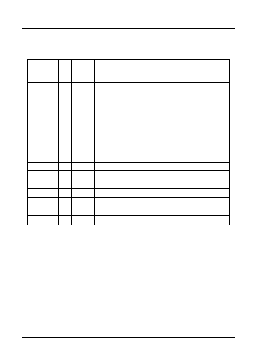
2. PIN INFORMATION
PIN ASSIGNMENTS AND PIN TYPE
Table 2.1 Pin Assignment and Pin type
Pin Signal
Pin
Type
Pin Signal
Pin
Type
1
/RESET I
2
GND Ground
3
D07 I/O 4
D08 I/O
5
D06 I/O 6
D09 I/O
7
D05 I/O 8
D10 I/O
9
D04 I/O 10
D11 I/O
11
D03 I/O 12
D12 I/O
13
D02 I/O 14
D13 I/O
15
D01 I/O 16
D14 I/O
17
D00 I/O 18
D15 I/O
19
GND DC 20
Key Pin
--
21
INPACK --
22
GND Ground
23
/IOW I 24
GND Ground
25
/IOR I 26
GND Ground
27
IORDY O 28
Reserved --
29
REG -- 30
GND Ground
31
IRQ O 32
/IOIS16 O
33
A01 I 34
/PDIAG I/O
35
A00 I 36
A02 I
37
/CS0 I 38
/CS1 I
39
/DASP I/O 40
GND Ground
HANBit HFDOM44MVxxx
URL:www.hbe.co.kr 5 / 13 HANBit Electronics Co., Ltd.
Rev. 1.0 (July. 2004)
Signal Descriptions
Table 2.2 Signal Descriptions
Signal Name
Dir.
Pin
Description
A[2:0]
I 33,35,36
In True IDE Mode only A[2:0] are used to select the one of eight registers in
the Task File, the remaining address lines should be grounded by the host.
-PDIAG
I/O
34
This input / output is the Pass Diagnostic signal in the Master / Slave
handshake protocol.
-DASP
I/O
39
In the True IDE Mode, this input/output is the Disk Active/Slave
Present signal in the Master/Slave handshake protocol.
-CS0, -CS1
I 37,38
CS0 is the chip select for the task file registers while CS2 is used to select
the Alternate Status Register and the Device Control Register.
D[15:00]
I/O
3,4,5,6,
7,8,9,10,
11,12,13,
14,15,16,
17,18
All Task File operations occur in byte mode on the low order bus D00-D07
while all data transfers are 16 bit using D00-D15.
GND
--
2,19,22,
24,26,
30,40,
Ground.
-IOR
I 25
This is an I/O Read strobe generated by the host.
-IOW
I 23
The I/O Write strobe pulse is used to clock I/O data on the Card Data bus
into the Storage Card controller registers when the Storage Card is
configured to use the I/O interface. The clocking will occur on the negative to
positive edge of the signal (trailing edge).
IRQ
O 31
In True IDE Mode signal is the active high Interrupt Request to the host.
-RESET
I 1
This input pin is the active low hardware reset from the host.
IORDY
O 27
This output signal may be used as IORDY.
-IOIS16
O 32
This output signal is asserted low when this device is expecting a word data
transfer cycle.

HANBit HFDOM44MVxxx
URL:www.hbe.co.kr 6 / 13 HANBit Electronics Co., Ltd.
Rev. 1.0 (July. 2004)
BLOCK DIAGRAM
PCMCIA
ATA
Interface
8051
Controller
Address
Decoder
ECC
FLASH
HOST
NAND
FLASH
DEVICE
NAND
FLASH
DEVICE
NAND
FLASH
DEVICE
NAND
FLASH
DEVICE
HOST
Interface
ECC
FLASH
HOST
NAND
FLASH
DEVICE
NAND
FLASH
DEVICE
NAND
FLASH
DEVICE
NAND
FLASH
DEVICE
MUX
Program
RAM
Data
RAM
Buffer
Program
ROM
A Channel
B Channel
Figure 2.1 Block Diagram
HANBit HFDOM44MVxxx
URL:www.hbe.co.kr 7 / 13 HANBit Electronics Co., Ltd.
Rev. 1.0 (July. 2004)
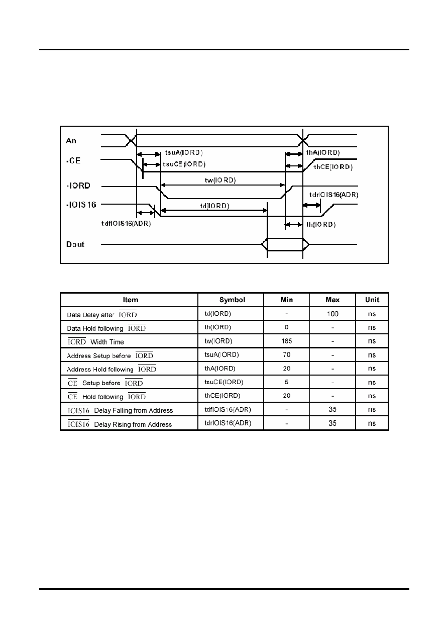
3. INTERFACE BUS TIMING
ACCESS SPCIFICATIONS
True IDE Mode I/O Read Timing
Table 3.1 True IDE Read Timing

HANBit HFDOM44MVxxx
URL:www.hbe.co.kr 8 / 13 HANBit Electronics Co., Ltd.
Rev. 1.0 (July. 2004)
True IDE Mode I/O Write Timing
Table 3.2 True IDE Write Timing

HANBit HFDOM44MVxxx
URL:www.hbe.co.kr 9 / 13 HANBit Electronics Co., Ltd.
Rev. 1.0 (July. 2004)
4. CONFIGURATION OPTION REGISTER
Overview
ATA register set definitions
(1) . Error Register
(2) . Device/Head Register
(3) . Status & Alternate Status Register
(4) . Device Control Register
(5) . Card Address Register
(6) . Data Register
(7) . Feature Register
(8) . Sector Count Register
(9) . Sector Number Register
(10) . Cylinder low register
(11) . Cylinder high register
PCMCIA Register Set Definitions
(1) . PCMCIA Configuration Option Register
(2) . PCMCIA Configuration and Status Register
(3) . PCMCIA pin Replacement Register
(4) . PCMCIA Socket and Copy Register
ATA Register Set Definitions:
Error Register
This register contains additional information about the source of an error when an error is indicated in bit 0
of the Status register. The bits are defined as follows:
D7
D6
D5
D4
D3
D2
D1
D0
BBK
UNC
0
IDNF
0
ABRT
0
AMNF
This register is also accessed on data bits D15-D8 during a write operation to offset 0 with -CE2 low and
-CE1 high.
Bit 7 (BBK): This bit is set when a Bad Block is detected.
Bit 6 (UNC): This bit is set when an Uncorrectable Error is encountered.
Bit 5: This bit is 0.
Bit 4 (IDNF): The requested sector ID is in error or cannot be found.
Bit 3: This bit is 0.
Bit 2 (Abort): This bit is set if the command has been aborted because of a CompactFlash Storage Card
status condition: (Not Ready, Write Fault, etc.) or when an invalid command has been issued.
Bit 1 This bit is 0.
Bit 0 (AMNF) This bit is set in case of a general error.
Device/Head Register
The Drive/Head register is used to select the drive and head. It is also used to select LBA addressing
instead of cylinder/head/sector addressing. The bits are defined as follows:
D7
D6
D5
D4
D3
D2
D1
D0
1
LBA
1
DRV
HS3
HS2
HS1
HS0
Bit 7: This bit is set to 1.
Bit 6: LBA is a flag to select either Cylinder/Head/Sector (CHS) or Logical Block Address Mode (LBA).
When LBA=0, Cylinder/Head/Sector mode is selected. When LBA=1, Logical Block Address is
selected. In Logical Block Mode, the Logical Block Address is interpreted as follows:
LBA7-LBA0: Sector Number Register D7-D0.
LBA15-LBA8: Cylinder Low Register D7-D0.
LBA23-LBA16: Cylinder High Register D7-D0.
LBA27-LBA24: Drive/Head Register bits HS3-HS0.
HANBit HFDOM44MVxxx
URL:www.hbe.co.kr 10 / 13 HANBit Electronics Co., Ltd.
Rev. 1.0 (July. 2004)
Bit 5: This bit is set to 1.
Bit 4 (DRV): DRV is the drive number. When DRV=0, drive (card) 0 is selected. When DRV=1, drive (card)
1 is selected. The CompactFlash Storage Card is set to be Card 0 or 1 using the copy field
(Drive #) of the PCMCIA Socket & Copy configuration register.
Bit 3 (HS3): When operating in the Cylinder , Head, Sector mode, this is bit 3 of the head number. It is Bit
27 in the Logical Block Address mode.
Bit 2 (HS2): When operating in the Cylinder, Head, Sector mode, this is bit 2 of the head number. It is Bit
26 in the Logical Block Address mode.
Bit 1 (HS1): When operating in the Cylinder, Head, Sector mode, this is bit 1 of the head number. It is Bit
25 in the Logical Block Address mode.
Bit 0 (HS0): When operating in the Cylinder, Head, Sector mode, this is bit 0 of the head number. It is Bit
24 in the Logical Block Address mode.
Status & Alternate Status Register
These registers return the CompactFlash Storage Card status when read by the host. Reading the Status
register does clear a pending interrupt while reading the Auxiliary Status register does not. The status bits
are described as follows:
D7
D6
D5
D4
D3
D2
D1
D0
BUSY
RDY
DWF
DSC
DRQ
CORR
0
ERR
Bit 7 (BUSY): The busy bit is set when the CompactFlash Storage Card has access to the command buffer
and registers and the host is locked out from accessing the command register and buffer. No
other bits in this register are valid when this bit is set to a 1.
Bit 6 (RDY): RDY indicates whether the device is capable of performing CompactFlash Storage Card
operations. This bit is cleared at power up and remains cleared until the CompactFlash
Storage Card is ready to accept a command.
Bit 5 (DWF): This bit, if set, indicates a write fault has occurred.
Bit 4 (DSC): This bit is set when the CompactFlash Storage Card is ready.
Bit 3 (DRQ): The Data Request is set when the CompactFlash Storage Card requires that information be
transferred either to or from the host through the Data register.
Bit 2 (CORR): This bit is set when a Correctable data error has been encountered and the data has been
corrected. This condition does not terminate a multi-sector read operation.
Bit 1 (IDX): This bit is always set to 0.
Bit 0 (ERR): This bit is set when the previous command has terminated with some type of error. The bits in
the Error register contain additional information describing the error. It is recommended that
media access commands (such as Read Sectors and Write Sectors) that end with an error
condition should have the address of the first sector in error in the command block registers.
Device Control Register
This register is used to control the CompactFlash Storage Card interrupt request and to issue an ATA soft
reset to the card. This register can be written even if the device is BUSY. The bits are defined as follows:
D7
D6
D5
D4
D3
D2
D1
D0
X
X
X
X
1
SW Rst
-IEn
0
Bit 7: This bit is an X (don't care).
Bit 6: This bit is an X (don't care).
Bit 5: This bit is an X (don't care).
Bit 4: This bit is an X (don't care).
Bit 3: This bit is ignored by the CompactFlash Storage Card.
Bit 2 (SW Rst): This bit is set to 1 in order to force the CompactFlash Storage Card to perform an AT Disk
controller Soft Reset operation. This does not change the PCMCIA Card Configuration
Registers (4.3.2 to 4.3.5) as a hardware Reset does. The Card remains Reset until this bit
is reset to `0.'
Bit 1 (-IEn): The Interrupt Enable bit enables interrupts when the bit is 0. When the bit is 1, interrupts from
the CompactFlash Storage Card are disabled. This bit also controls the Int bit in the
Configuration and Status Register. This bit is set to 0 at power on and Reset.
Bit 0: This bit is ignored by the CompactFlash Storage Card.

HANBit HFDOM44MVxxx
URL:www.hbe.co.kr 11 / 13 HANBit Electronics Co., Ltd.
Rev. 1.0 (July. 2004)
Card Address Register
This register is provided for compatibility with the AT disk drive interface. It is recommended that this
register not be mapped into the host's I/O space because of potential conflicts on Bit 7. The bits are defined
as follows:
D7
D6
D5
D4
D3
D2
D1
D0
X
-WTG
-HS3
-HS2
-HS1
-HS0
-nDS1
-nDS0
Bit 7: This bit is reserved.
Implementation Note:
Conflicts may occur on the host data bus when this bit is provided by a Floppy Disk Controller
operating at the same addresses as the CompactFlash Storage Card. Following are some possible
solutions to this problem for the PCMCIA implementation:
1) Locate the CompactFlash Storage Card at a non-conflicting address, i.e. Secondary address (377)
or in an independently decoded Address Space when a Floppy Disk Controller is located at the
Primary addresses.
2) Do not install a Floppy and a CompactFlash Storage Card in the system at the same time.
3) Implement a socket adapter which can be programmed to (conditionally) tri-state D7 of I/0 address
3F7h/377h when a CompactFlash Storage Card is installed and conversely to tri-state
D6-D0 of I/O addresses 3F7h/377h when a floppy controller is installed.
4) Do not use the CompactFlash Storage Card's Drive Address register. This may be accomplished
by either a) If possible, program the host adapter to enable only I/O addresses 1F0h-1F7h, 3F6h (or
170h-177h, 176h) to the CompactFlash Storage Card or b) if provided use an additional Primary /
Secondary configuration in the CompactFlash Storage Card which does not respond to accesses to
I/O locations 3F7h and 377h. With either of these implementations, the host software must not
attempt to use information in the Drive Address Register.
Bit 6 (-WTG): This bit is 0 when a write operation is in progress, otherwise, it is 1.
Bit 5 (-HS3): This bit is the negation of bit 3 in the Drive/Head register.
Bit 4 (-HS2): This bit is the negation of bit 2 in the Drive/Head register.
Bit 3 (-HS1): This bit is the negation of bit 1 in the Drive/Head register.
Bit 2 (-HS0): This bit is the negation of bit 0 in the Drive/Head register.
Bit 1 (-nDS1): This bit is 0 when drive 1 is active and selected.
Bit 0 (-nDS0): This bit is 0 when the drive 0 is active and selected.
Data Register
The Data Register is a 16-bit register, and it is used to transfer data blocks between the CompactFlash
Storage Card data buffer and the Host. This register overlaps the Error Register. The table below describes
the combinations of data register access and is provided to assist in understanding the overlapped Data
Register and Error/Feature Register rather than to attempt to define general PCMCIA word and byte
access modes and operations. See the PCMCIA PC Card Standard Release 2.0 for definitions of the Card
Accessing Modes for I/O and Memory cycles.
15
14
13
12
11
10
9
8
Data (15:8)
7
6
5
4
3
2
1
0
Data (7:0)
Feature Register
This register provides information regarding features of the CompactFlash Storage Card that the
host can utilize. This register is also accessed on data bits D15-D8 during a write operation to
Offset 0 with -CE2 low and -CE1 high.
7
6
5
4
3
2
1
0
Command specific

HANBit HFDOM44MVxxx
URL:www.hbe.co.kr 12 / 13 HANBit Electronics Co., Ltd.
Rev. 1.0 (July. 2004)
Sector Count Register
This register contains the numbers of sectors of data requested to be transferred on a read or write
operation between the host and the CompactFlash Storage Card. If the value in this register is zero, a
count of 256 sectors is specified. If the command was successful, this register is zero at command
completion. If not successfully completed, the register contains the number of sectors that need to be
transferred in order to complete the request.
7
6
5
4
3
2
1
0
Sector Count
Sector Number Register
This register contains the starting sector number or bits 7-0 of the Logical Block Address (LBA) for any
CompactFlash Storage Card data access for the subsequent command.
BIT DESCRIPTION -----
CHS
7
6
5
4
3
2
1
0
Sector (7:0)
LBA
7
6
5
4
3
2
1
0
LBA (15:8)
Cylinder Low Register
This register contains the low order 8 bits of the starting cylinder address or bits 15-8 of the Logical Block Address.
BIT DESCRIPTION-----
CHS
7
6
5
4
3
2
1
0
Cylinder (7:0)
LBA
7
6
5
4
3
2
1
0
LBA (15:8)
Cylinder High Register
This register contains the high order bits of the starting cylinder address or bits 23-16 of the Logical Block Address.
BIT DESCRIPTION -
CHS
7
6
5
4
3
2
1
0
Cylinder (7:0)
LBA
7
6
5
4
3
2
1
0
LBA (15:8)
HANBit HFDOM44MVxxx
URL:www.hbe.co.kr 13 / 13 HANBit Electronics Co., Ltd.
Rev. 1.0 (July. 2004)
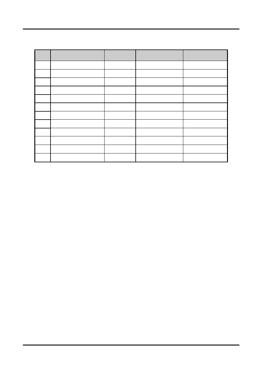
Ordering Infomation
NO
Parts
Capacity
Media transfer
mode
Operation
Mode
1
DOM44MV016
16Mbyte BYTE
True IDE
2
DOM44MV032
32Mbyte BYTE
True IDE
3
DOM44MV064
64Mbyte BYTE
True IDE
4
DOM44MV096
96Mbyte BYTE
True IDE
5
DOM44MV128
128Mbyte BYTE
True IDE
6
DOM44MV192
192Mbyte BYTE
True IDE
7
DOM44MV256
256Mbyte BYTE
True IDE
8
DOM44MV384
384Mbyte BYTE
True IDE
9
DOM44MV512
512Mbyte BYTE
True IDE
10
DOM44MV768
768byte BYTE
True IDE
11
DOM44MV1G
1Gbyte BYTE
True IDE
12
DOM44MV1.5G
1.5Gbyte BYTE
True IDE