
HANBit HDD32M64F8K
URL : www.hbe.co.kr 1 HANBit Electronics Co.,Ltd.
REV 1.0 (August.2002)
GENERAL DESCRIPTION
The HDD32M64F8K is a 32M x 64 bit Double Data Rate(DDR) Synchronous Dynamic RAM high-density memory module.
The module consists of sixteen CMOS 16M x 8 bit with 4banks DDR SDRAMs in 66pin TSOP-II 400mil packages and 2K
EEPROM in 8-pin TSSOP package on a 200-pin glass-epoxy. Four 0.1uF decoupling capacitors are mounted on the printed
circuit board in parallel for each DDR SDRAM. The HSD32M64F8K is a SMM(Stackable Memory Module
type) .Synchronous design allows precise cycle control with the use of system clock. Data I/O transactions are possible on
both edges of DQS. Range of operating frequencies, programmable latencies and burst lengths allows the same device to
be useful for a variety of high bandwidth, high performance memory system applications. All module components may be
powered from a single 2.5V DC power supply and all inputs and outputs are SSTL_2 compatible.
FEATURES
∑
Part Identification
HDD32M64F8K
≠
10A : 100MHz (CL=2)
HDD32M64F8K
≠
13A : 133MHz (CL=2)
HDD32M64F8K
≠
13B : 133MHz (CL=2.5)
∑
256MB(32Mx64) Unbuffered DDR SMM based on 16Mx8 DDR SDRSM
∑
2.5V
±
0.2V VDD and VDDQ power supply
∑
Auto & self refresh capability (4096 Cycles/64ms)
∑
All input and output are compatible with SSTL_2 interface
∑
Data(DQ), Data strobes and write masks latched on the rising and falling edges of the clock
∑
All Addresses and control inputs except Data(DQ), Data strobes and Data masks latched on the rising edges of the clock
∑
MRS cycle with address key programs
- Latency (Access from column address) : 2, 2.5
- Burst length : 2, 4, 8
- Data scramble : Sequential & Interleave
∑
Data(DQ), Data strobes and write masks latched on the rising and falling edges of the clock
∑
All Addresses and control inputs except Data(DQ), Data strobes and Data masks latched on the rising edges of the clock
∑
The used device is 4M x 8bit x 4Banks DDR SDRAM
DDR SDRAM Module 256Mbyte (32Mx64bit), based on16Mx8,4Banks,
4K Ref., SMM, Part No. HDD32M64F8K
HANBit HDD32M64F8K
URL : www.hbe.co.kr 2 HANBit Electronics Co.,Ltd.
REV 1.0 (August.2002)
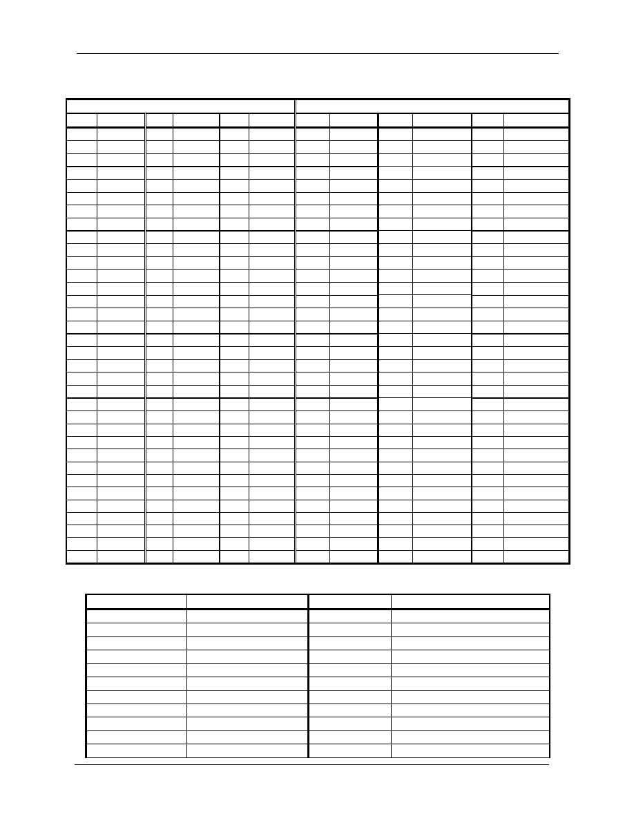
PIN ASSIGNMENT
P1
P2
PIN
Symbol
PIN
Symbol
PIN
Symbol
PIN
Symbol
PIN
Symbol
PIN
Symbol
1
/CS0
35
DQ15
69
NC
1
VDDQ
35
DQ17
69
NC(DQS8)
2
/CS1
36
DQ14
70
DQS1
2
A3
36
DQ18
70
DQS3
3
VSS
37
VDDQ
71
DQS5
3
VSS
37
VDDQ
71
DQS6
4
CKE0
38
DQ13
72
VDD
4
A2
38
DQ19
72
VDD
5
CKE1
39
DQ12
73
NC
5
A1
39
DQ20
73
DQ56
6
NC
40
DQ11
74
DQ39
6
A0
40
DQ21
74
DQ57
7
VDD
41
VSS
75
DQ38
7
VDD
41
VSS
75
DQ58
8
CK0
42
DQ10
76
VSS
8
A10
42
DQ22
76
VSS
9
CK1
43
DQ9
77
DQ37
9
A11
43
DQ23
77
DQ59
10
NC
44
DQ8
78
DQ36
10
BA0
44
NC(CB6)
78
DQ60
11
VSS
45
VDD
79
VDDQ
11
VSS
45
VDD
79
VDDQ
12
NC
46
*SA0
80
DQ35
12
BA1
46
NC(CB4)
80
DQ61
13
DM0
47
*SA1
81
DQ34
13
DM2
47
NC(CB2)
81
DQ62
14
DM4
48
VSS
82
DQ33
14
DM6
48
VSS
82
DQ63
15
VDDQ
49
*SA2
83
VSS
15
VDDQ
49
NC(CB0)
83
VSS
16
NC
50
VDDQ
84
DQ32
16
NC
50
VDDQ
84
DQ55
17
NC
51
VDD
85
DQ40
17
NC
51
VDD
85
DQ54
18
VSS
52
/RAS
86
DQ41
18
VSS
52
A4
86
DQ53
19
NC
53
VSS
87
VDDQ
19
DQS7
53
VSS
87
VDDQ
20
DQS0
54
/CAS
88
DQ42
20
DQS2
54
A5
88
DQ52
21
DQS4
55
/CK0
89
DQ43
21
NC
55
A6
89
DQ51
22
VDD
56
/CK1
90
DQ44
22
VDD
56
A7
90
DQ50
23
NC
57
VDD
91
VSS
23
DQ31
57
VDD
91
VSS
24
DQ0
58
/CK2
92
DQ45
24
DQ30
58
A8
92
DQ49
25
DQ1
59
CK2
93
DQ46
25
DQ29
59
A9
93
DQ48
26
VSS
60
/WE
94
DQ47
26
VSS
60
NC(A12)
94
NC(CB7)
27
DQ2
61
VSS
95
*SCL
27
DQ28
61
VSS
95
VDD
28
DQ3
62
NC
96
*WP
28
DQ27
62
DM3
96
NC(CB5)
29
VDDQ
63
DM1
97
*VSPD
29
VDDQ
63
DM7
97
NC(CB3)
30
DQ4
64
DM5
98
VSS
30
DQ26
64
NC(DM8)
98
VSS
31
DQ5
65
VDDQ
99
*SDA
31
DQ25
65
VDDQ
99
NC(CB1)
32
DQ6
66
NC
100
VDDIN
32
DQ24
66
NC
100
VDD
33
VSS
67
VREF
33
VSS
67
NC(A13)
34
DQ7
68
VSS
34
DQ16
68
VSS
* These pins should be NC in the system which does not support SPD
PIN
PIN DESCRIPTION
PIN
PIN DESCRIPTION
A0~A11
Address input
VDD
Power supply(2.5V)
BA0~BA1
Bank Select Address
VDDQ
Power supply for DQs(2.5V)
DQ0~DQ63
Data input/output
VREF
Power supply for reference
CB0~CB7
Check bit(Data input/output)
VSPD
Serial EEPROM Power supply(3.3)
DQS0~DQS7
Data Strobe input/output
VSS
Ground
DM0~DM7
Data-in Mask
SA0~SA2
Address in EEPROM
CK0~CK2,/CK0~/CK2
Clock input
SDA
Serial data I/O
CKE0~CKE1
Clock enable input
SCL
Serial clock
/CS0~/CS1
Chip Select input
WP
Write protection
/RAS
Row Address strobe
VDDIN
VDD indentification flag
/CAS
Column Address strobe
NC
No connection
HANBit HDD32M64F8K
URL : www.hbe.co.kr 3 HANBit Electronics Co.,Ltd.
REV 1.0 (August.2002)
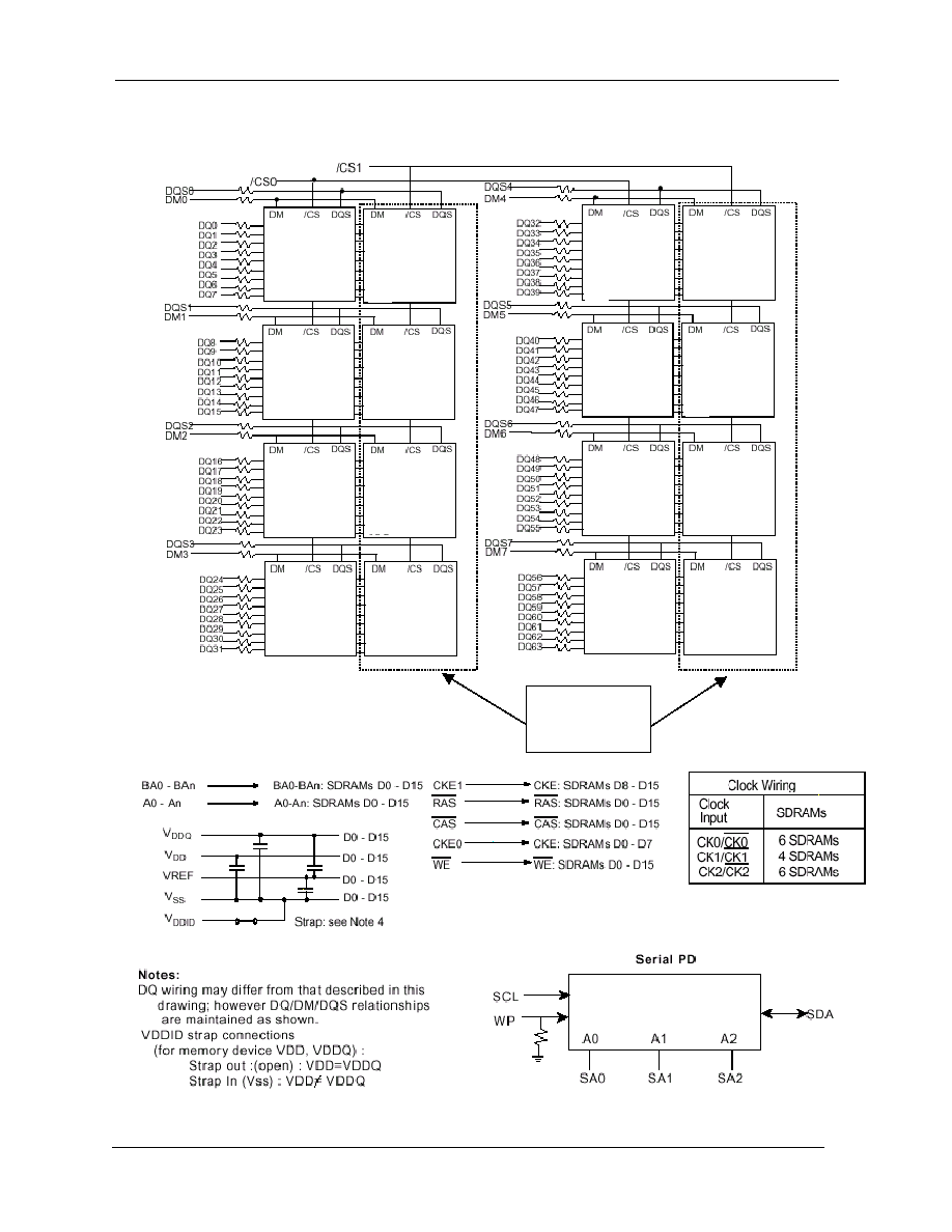
U1
U2
U3
U4
U5
U6
U8
U9
U10
U11
U13
U14
U15
U16
U18
U19
I/O 0
I/O 1
I/O 2
I/O 3
I/O 4
I/O 5
I/O 6
I/O 7
I/O 0
I/O 1
I/O 2
I/O 3
I/O 4
I/O 5
I/O 6
I/O 7
I/O 0
I/O 1
I/O 2
I/O 3
I/O 4
I/O 5
I/O 6
I/O 7
I/O 0
I/O 1
I/O 2
I/O 3
I/O 4
I/O 5
I/O 6
I/O 7
I/O 0
I/O 1
I/O 2
I/O 3
I/O 4
I/O 5
I/O 6
I/O 7
I/O 0
I/O 1
I/O 2
I/O 3
I/O 4
I/O 5
I/O 6
I/O 7
I/O 0
I/O 1
I/O 2
I/O 3
I/O 4
I/O 5
I/O 6
I/O 7
I/O 0
I/O 1
I/O 2
I/O 3
I/O 4
I/O 5
I/O 6
I/O 7
I/O 0
I/O 1
I/O 2
I/O 3
I/O 4
I/O 5
I/O 6
I/O 7
I/O 0
I/O 1
I/O 2
I/O 3
I/O 4
I/O 5
I/O 6
I/O 7
I/O 0
I/O 1
I/O 2
I/O 3
I/O 4
I/O 5
I/O 6
I/O 7
I/O 0
I/O 1
I/O 2
I/O 3
I/O 4
I/O 5
I/O 6
I/O 7
I/O 0
I/O 1
I/O 2
I/O 3
I/O 4
I/O 5
I/O 6
I/O 7
I/O 0
I/O 1
I/O 2
I/O 3
I/O 4
I/O 5
I/O 6
I/O 7
I/O 0
I/O 1
I/O 2
I/O 3
I/O 4
I/O 5
I/O 6
I/O 7
I/O 0
I/O 1
I/O 2
I/O 3
I/O 4
I/O 5
I/O 6
I/O 7
Stacking
FUNCTIONAL BLOCK DIAGRAM

HANBit HDD32M64F8K
URL : www.hbe.co.kr 4 HANBit Electronics Co.,Ltd.
REV 1.0 (August.2002)
PIN FUNCTION DESCRIPTION
Pin
Name
Input Function
CK, /CK
Clock
CK and CK are differential clock inputs. All address and control input signals are
sam-pled on the positive edge of CK and negative edge of CK. Output (read) data
is referenced to both edges of CK. Internal clock signals are derived from CK/CK.
CKE
Clock Enable
CKE HIGH activates, and CKE LOW deactivates internal clock signals, and
device input buffers and output drivers. Deactivating the clock provides
PRECHARGE
POWER-DOWN and SELF REFRESH operation (all banks idle), or ACTIVE
POWER-DOWN(row ACTIVE in any bank). CKE is synchronous for all functions
except for disabling outputs, which is achieved asynchronously. Input buffers,
excluding CK, CK and CKE are disabled during power-down and self refresh
modes, providing low standby power. CKE will recognizean LVCMOS LOW level
prior to VREF being stable on power-up.
/CS
Chip Select
CS enables(registered LOW) and disables(registered HIGH) the command
decoder.
All commands are masked when CS is registered HIGH. CS provides for external
bank selection on systems with multiple banks. CS is considered part of the
command code.
A0 ~ A11
Address
Row/column addresses are multiplexed on the same pins.
Row address : RA0 ~ RA11, Column address : CA0 ~ CA9
BA0 ~ BA1 Bank select address
BA0 and BA1 define to which bank an ACTIVE, READ, WRITE or PRE-CHARGE
command is being applied.
/RAS
Row address strobe
Latches row addresses on the positive going edge of the CLK with /RAS low.
Enables row access & precharge.
/CAS
Columnaddress strobe
Latches column addresses on the positive going edge of the CLK with /CAS low.
Enables column access.
/WE
Write enable
Enables write operation and row precharge.
Latches data in starting from /CAS, /WE active.
DQS0 ~ 7
Data Strobe
Output with read data, input with write data. Edge-aligned with read data, cen-
tered in write data. Used to capture write data.
DM0~7
Input Data Mask
DM is an input mask signal for write data. Input data is masked when DM is
sampled HIGH along with that input data during a WRITE access. DM is sampled
on both edges of DQS. DM pins include dummy loading internally, to matches the
DQ and DQS load-ing.
DQ0 ~ 63
Data input/output
Data inputs/outputs are multiplexed on the same pins.
WP
Write Protection
WP pin is connected to Vcc.
When WP is
"
high
"
, EEPROM Programming will be inhibited and the entire
memory will be write-protected.
VDDQ
Supply
DQ Power Supply : +2.5V
±
0.2V.
VDD
Supply
Power Supply : +2.5V
±
0.2V (device specific).
VSS
Supply
DQ Ground.
VREF
Supply
SSTL_2 reference voltage.
HANBit HDD32M64F8K
URL : www.hbe.co.kr 5 HANBit Electronics Co.,Ltd.
REV 1.0 (August.2002)
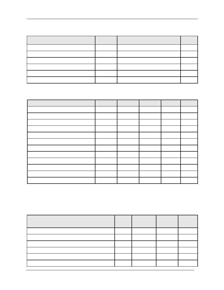
ABSOLUTE MAXIMUM RATINGS
PARAMETER
SYMBOL
RATING
UNTE
Voltage on any pin relative to Vss
V
IN
, V
OUT
-o.5 ~ 3.6
V
Voltage on V
DD
supply relative to Vss
V
DD
-1.0 ~ 3.6
V
Voltage on V
DDQ
supply relative to Vss
V
DDQ
-0.5 ~ 3.6
V
Storage temperature
T
STG
-55 ~ +150
∞
C
Power dissipation
P
D
16.0
W
Short circuit current
I
OS
50
mA
Notes: Operation at above absolute maximum rating can adversely affect device reliability
DC OPERATING CONDITIONS
(Recommended operating conditions (Voltage referenced to Vss = 0V, T
A
= 0 to 70
∞
C) )
PARAMETER
SYMBOL
MIN
MAX
UNIT
NOTE
Supply Voltage
V
DD
2.3
2.7
V
I/O Supply Voltage
V
DDQ
2.3
2.7
V
I/O Reference Voltage
V
REF
1.15
1.35
V
1
I/O Termination Voltage(system)
V
TT
V
REF
≠
0.04
V
REF
+ 0.04
V
2
Input High Voltage
V
IH
(DC)
V
REF
+ 0.15
V
REF
+ 0.3
V
Input Low Voltage
V
IL
(DC)
-0.3
V
REF
- 0.15
V
Input Voltage Level, CK and /CK inputs
V
IN
(DC)
-0.3
V
DDQ
+ 0.3
V
Input Differential Voltage, CK and /CK inputs
V
ID
(DC)
0.3
V
DDQ
+ 0.6
V
Input leakage current
I
LI
-2
2
uA
3
Output leakage current
I
OZ
-5
5
uA
Output High current (V
OUT
= 1.95V)
I
OH
-16.8
mA
Output Low current (V
OUT
= 0.35V)
I
OL
16.8
mA
Notes :
1.Typically, the value of V
REF
is expected to be about 0.5* V
DD
of the transmitting device.
V
REF
is expected to track variation in V
DDQ .
2.Peak to peak AC noise on V
REF
may not exceed
2% V
REF
(DC).
3.V
TT
of the transmitting device must track V
REF
of the receiving device.
CAPACITANCE
(V
DD
= min to max, V
DDQ
= 2.5V
to 2.7V, T
A
= 25
∞
C, f = 100MHz)
DESCRIPTION
SYMBO
L
MIN
MAX
UNITS
Input capacitance(A0~A11, BA0~BA1, /RAS, /CAS,/WE)
C
IN1
93
107
pF
Input capacitance(CKE0,CKE1)
C
IN2
63
77
pF
Input capacitance(/CS0~/CS1)
C
IN3
58
72
pF
Input capacitance(CLK0, CLK1,CLK2)
C
IN4
30
45
pF
Input capacitance(DM0~DM7)
C
IN5
10
15
pF
Data input/output capacitance (DQ0 ~ DQ63, DQS0~DQS7)
C
OUT1
10
15
pF

HANBit HDD32M64F8K
URL : www.hbe.co.kr 6 HANBit Electronics Co.,Ltd.
REV 1.0 (August.2002)
DC CHARACTERISTICS
(Recommended operating condition unless otherwise noted, V
DD
= 2.5V, T =25
∞
C)
VERSION
NOTE
PARAMETER
SYMBO
L
TEST
CONDITION
-10A
-13A
-13B
UNIT
Operating current
(One bank active)
I
DD1
Burst length = 2
t
RC
t
RC
(min), CL=2.5
I
OUT
= 0mA,
Active-Read-Presharge
1520
1600
1600
mA
Precharge standby
current in
power-down mode
I
DD2P
CKE
V
IL
(max)
t
CK
= tCK(min), All banks
idle
48
56
56
mA
Precharge
standby current in
non power-down mode
I
DD2N
CKE
V
IH
(min)
/CS
V
IH
(min), t
CK
= tCK(min)
288
320
320
mA
Active standby current in
power-down mode
I
DD3P
All banks idle, CKE
V
IL
(max), t
CK
= tCK(min)
480
560
560
mA
Active standby current in
non power-down mode
(One bank active)
I
DD3N
Onel banks,
Active-Read-Presharge,
t
RC
=t
RAS
(max),
t
CK
=
tCK(min)
720
800
800
mA
CL=2.
5
Operating current (Read)
I
DD4R
Burst length = 2
t
RC
= t
RC
(min),
I
OUT
= 0mA,
CL=2
1840
2160
2160
mA
CL=2.
5
Operating current (Write)
I
DD4W
Burst length = 2
t
RC
= t
RC
(min)
CL=2
1840
2240
2240
mA
Auto refresh current
I
DD5
t
RC
t
REF
(min)
2720
2880
2880
mA
Self refresh current
I
DD6
CKE
0.2V
32
32
32
mA
AC OPERATING CONDITIONS
PARAMETER
STMBOL
MIN
MAX
UNIT
NOTE
Input High (Logic 1) Voltage, DQ, DQS and DM signals
V
IH
(AC)
VREF + 0.35
Input Low (Logic 0) Voltage, DQ, DQS and DM signals.
V
IL
(AC)
VREF - 0.35
V
Input Differential Voltage, CK and CK inputs
V
ID
(AC)
0.7
VDDQ+0.6
V
1
Input Crossing Point Voltage, CK and CK inputs
V
IX
(AC)
0.5*VDDQ-0.2
0.5*VDDQ+0.2
V
2
Notes:
1. VID is the magnitude of the difference between the input level on CK and the input on CK.
2.
The value of V
IX
is expected to equal 0.5* V
DDQ
of the transmitting device and must track variations in the DC level
of the same

HANBit HDD32M64F8K
URL : www.hbe.co.kr 7 HANBit Electronics Co.,Ltd.
REV 1.0 (August.2002)
AC OPERATING TEST CONDITIONS
PARAMETER
VALUE
UNIT
NOTE
Input reference voltage for Clock
0.5 * V
DDQ
V
Input signal maximum peak swing
1.5
V
Input signal minimum slew rate
1.0
V
Input Levels(V
IH
/V
IL
)
V
REF
+0.35/V
REF
V
Input timing measurement reference level
V
REF
V
Output timing measurement reference level
V
TT
V
Output load condition
See Load Circuit
V
AC CHARACTERISTICS
(These AC charicteristics were tested on the Component)
DDR200
DDR266A
DDR266B
-10A
-13A
-13B
PARAMETER
SYMBO
L
MIN
MAX
MIN
MAX
MIN
MAX
UNIT NOTE
Row cycle time
t
RC
70
65
65
ns
1
Refresh row cycle time
t
RFC
80
75
75
ns
1,2
Row active time
t
RAS
48
120K
45
120K
45
120K
ns
1,2
/RAS to /CAS delay
t
RCD
20
20
20
ns
3
Row precharge time
t
RP
20
20
20
ns
3
Row active to Row active delay
t
RRD
15
15
15
ns
3
Write recovery time
t
WR
2
2
2
t
CK
3
Last data in to Read command
t
CDLR
1
1
1
t
CK
2
Col. address to Col. address delay
t
CCD
1
1
1
t
CK
CL=2.0
10
12
7.5
12
10
12
ns
Clock cycle time
CL=2.5
t
CK
12
7.5
12
7.5
12
ns
HANBit HDD32M64F8K
URL : www.hbe.co.kr 8 HANBit Electronics Co.,Ltd.
REV 1.0 (August.2002)
Clock high level width
t
CH
0.45
0.55
0.45
0.55
0.45
0.55
t
CK
Clock low level width
t
CL
0.45
0.55
0.45
0.55
0.45
0.55
t
CK
DQS-out access time from CK/CK
t
DQSCK
-0.8
+0.8
-0.75
+0.75
-0.75
+0.75
ns
Output data access time from CK/CK
t
AC
-0.8
+0.8
-0.75
+0.75
-0.75
+0.75
ns
Data strobe edge to ouput data edge
t
DQSQ
-
+0.6
-
+0.5
-
+0.5
ns
Read Preamble
t
RPRE
0.9
1.1
0.9
1.1
0.9
1.1
t
CK
Read Postamble
t
RPST
0.4
0.6
0.4
0.6
0.4
0.6
t
CK
Data out high impedence time from CK-
/CK
t
HZQ
-0.8
+0.8
-0.75
+0.75
-0.75
+0.75
ns
2
CK to valid DQS-in
t
DQSS
0.75
1.25
0.75
1.25
0.75
1.25
t
CK
DQS-in setup time
t
WPRES
0
0
0
ns
3
DQS-in hold time
t
WPREH
0.25
0.25
0.25
t
CK
DQS-in falling edge to CK rising-setup
time
t
DSS
0.2
0.2
0.2
t
CK
DQS-in falling edge to CK rising hold
time
t
DSH
0.2
0.2
0.2
t
CK
DQS-in high level width
t
DQSH
0.35
0.35
0.35
t
CK
DQS-in low level width
t
DQSL
0.35
0.35
0.35
t
CK
DQS-in cycle time
t
DSC
0.9
1.1
0.9
1.1
0.9
1.1
t
CK
Address and Control Input setup time
t
IS
1.1
0.9
0.9
ns
Address and Control Input hold time
t
IH
1.1
0.9
0.9
ns
Mode register set cycle time
t
MRD
16
15
15
ns
DQ & DM setup time to DQS
t
DS
0.6
0.5
0.5
ns
DQ & DM hold time to DQS
t
DH
0.6
0.5
0.5
ns
DQ & DM input pulse width
t
DIPW
2
1.75
1.75
ns
Power down exit time
t
PDEX
10
10
10
ns
Exit self refresh to write command
t
XSW
116
95
ns
Exit self refresh to bank active
command
t
XSA
80
75
75
ns
Exit self refresh to read command
t
XSR
200
200
200
Cycle
Refresh interval time
T
REF
15.6
15.6
15.6
us
1
Output DQS valid window
T
QH
0.35
0.35
0.35
t
CK
DQS write postamble time
T
WPST
0.25
0.25
0.25
t
CK
4
Notes :
1. Maximum burst refresh of 8.
2. t
HZQ
transitions occurs in the same assess time windows as valid data transitions. These parameters are not
referenced to a specific voltage level, but specify when the device output is no longer driving.
3. The specific requirement is that DQS be valid(High-Low) on or before this CK edge. The case shown(DQS going
from High_Z to logic Low) applies when no writes were previously in progress on the bus. If a previous write was
in progress, DQS could be High at this time, depending on t
DQSS.
HANBit HDD32M64F8K
URL : www.hbe.co.kr 9 HANBit Electronics Co.,Ltd.
REV 1.0 (August.2002)
4. The maximum limit for this parameter is not a device limit. The device will operate with a great value for this
parameter, but system performance (bus turnaround) will degrade accordingly.
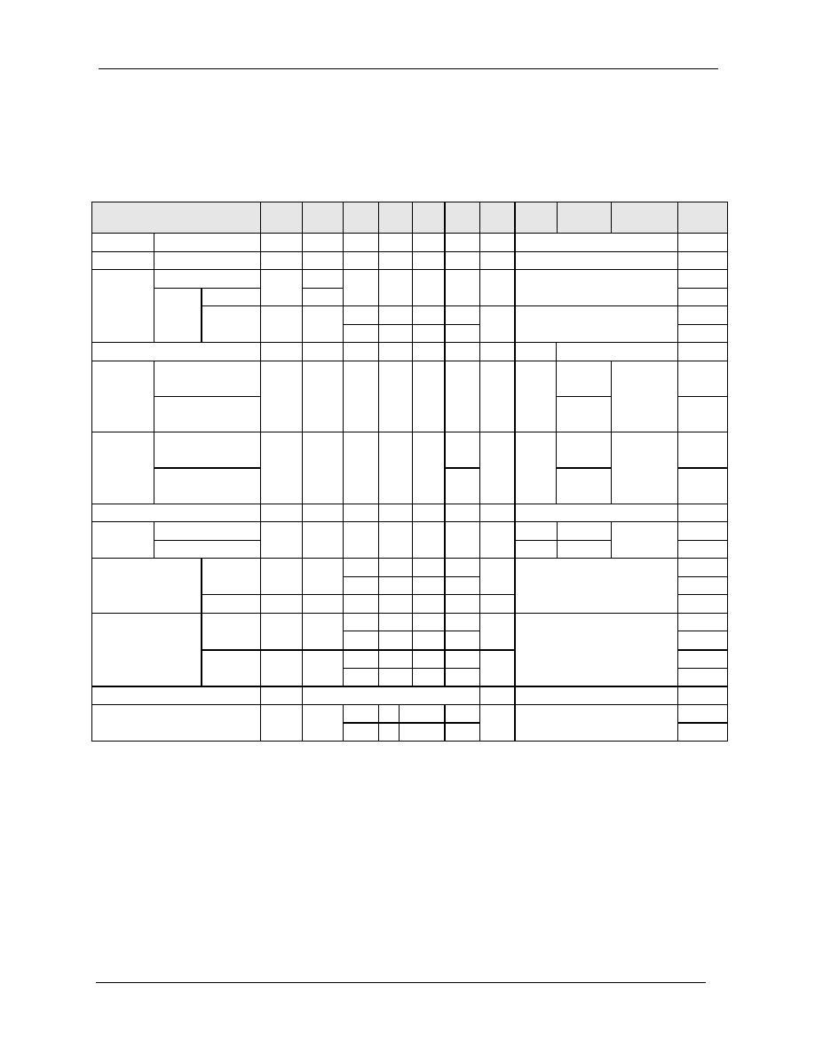
SIMPLIFIED TRUTH TABLE
COMMAND
CKE
n-1
CKE
n
/CS
/R
A
S
/C
A
S
/WE DM
BA
0,1
A10/
AP
A11
A9~A0
NOTE
Register
Extended MRS
H
X
L
L
L
L
X
OP code
1,2
Register
Mode register set
H
X
L
L
L
L
X
OP code
1,2
Auto refresh
H
3
Entry
H
L
L
L
L
H
X
X
3
L
H
H
H
3
Refresh
Self
refres
h
Exit
L
H
H
X
X
X
X
X
3
Bank active & row addr.
H
X
L
L
H
H
X
V
Row address
Auto
precharge
disable
L
4
Read &
column
address
Auto
precharge
eable
H
X
L
H
L
H
X
V
H
Column
Address
(A0 ~ A9)
4
Auto
precharge
disable
H
L
4
Write &
column
address
Auto
precharge
enable
H
X
L
H
L
L
X
V
H
Column
Address
(A0 ~ A9)
4,6
Burst Stop
H
X
L
H
H
L
X
X
7
Bank selection
V
L
Precharg
e
All banks
H
X
L
L
H
L
X
X
H
X
5
H
X
X
X
Entry
H
L
L
V
V
V
X
Clock suspend or
active power down
Exit
L
H
X
X
X
X
X
X
H
X
X
X
Entry
H
L
L
H
H
H
X
H
X
X
X
Precharge power
down mode
Exit
L
H
L
V
V
V
X
X
DM
H
X
V
X
8
H
X
X
X
No operation command
H
X
L
H
H
H
X
X
(V=Valid, X=Don't care, H=Logic high, L=Logic low)
Notes :
1. OP Code : Operand code
A0 ~ A11 & BA0 ~ BA1 : Program keys. (@ MRS)
2. MRS can be issued only at all banks precharge state.
A new command can be issued after 2 CLK cycles of MRS.
3. Auto refresh functions are as same as CBR refresh of DRAM.
The automatical precharge without row precharge command is meant by "Auto".
Auto/self refresh can be issued only at all banks precharge state.
4. BA0 ~ BA1 : Bank select addresses.
If both BA0 and BA1 are "Low" at read, write, row active and precharge, bank A is selected.
If both BA0 is "Low" and BA1 is "High" at read, write, row active and precharge, bank B is selected.
If both BA0 is "High" and BA1 is "Low" at read, write, row active and precharge, bank C is selected.
If both BA0 and BA1 are "High" at read, write, row active and precharge, bank D is selected.
If A10/AP is "High" at row precharge, BA0 and BA1 is ignored and all banks are selected.

HANBit HDD32M64F8K
URL : www.hbe.co.kr 10 HANBit Electronics Co.,Ltd.
REV 1.0 (August.2002)
5. During burst read or write with auto precharge, new read/write command can not be issued.
Another bank read/write command can be issued after the end of burst.
New row active of the associated bank can be issued at t
RP
after the end of burst.
6. Burst stop command is valid at every burst length.
7. DM sampled at the rising and falling edges of the DQS and Data-in are masked at the both edges
(Write DM latency is 0)
PACKAGING INFORMATION
Unit : mm
Front
≠
Side
Rear-Side

HANBit HDD32M64F8K
URL : www.hbe.co.kr 11 HANBit Electronics Co.,Ltd.
REV 1.0 (August.2002)
ORDERING INFORMATION
Part Number
Density
Org.
Package
Ref.
Vcc
MODE
MAX.frq
HDD32M64F8K-10A
256MByte
32M x 64
200PIN SMM
4K
2.5V
DDR
100MHz/CL2
HDD32M64F8K-13A
256MByte
32M x 64
200PIN SMM
4K
2.5V
DDR
133MHz/CL2
HDD32M64F8K-13B
256MByte
32M x 64
200PIN SMM
4K
2.5V
DDR
133MHz/CL2.5