HANBit HDD32M72B18RPW
URL : www.hbe.co.kr 1 HANBit Electronics Co.,Ltd.
REV 1.0 (August.2002)
GENERAL DESCRIPTION
The HDD32M72D18RPW is a 64M x 72 bit Double Data Rate(DDR) Synchronous Dynamic RAM high-density memory
module. The module consists of eighteen CMOS 16M x 8 bit with 4banks DDR SDRAMs in 66pin TSOP-II 400mil packages
and 2K EEPROM in 8-pin TSSOP package on a 184-pin glass-epoxy. Four 0.1uF decoupling capacitors are mounted on
the printed circuit board in parallel for each DDR SDRAM. The HDD32M72D18RPW is a DIMM(Dual in line Memory
Module) .Synchronous design allows precise cycle control with the use of system clock. Data I/O transactions are possible
on both edges of DQS. Range of operating frequencies, programmable latencies and burst lengths allows the same device
to be useful for a variety of high bandwidth, high performance memory system applications. All module components may be
powered from a single 2.5V DC power supply and all inputs and outputs are SSTL_2 compatible.
FEATURES
∑
Part Identification
HDD32M72B18RPW
≠
10A : 100MHz (CL=2)
HDD32M72B18RPW
≠
13A : 133MHz (CL=2)
HDD32M72B18RPW
≠
13B : 133MHz (CL=2.5)
∑
256MB(32Mx72) registered DDR DIMM based on 16Mx8 DDR SDRSM
∑
2.5V
±
0.2V VDD and VDDQ power supply
∑
Auto & self refresh capability (4K Cycles / 64ms)
∑
All input and output are compatible with SSTL_2 interface
∑
Data(DQ), Data strobes and write masks latched on the rising and falling edges of the clock
∑
All Addresses and control inputs except Data(DQ), Data strobes and Data masks latched on the rising edges of the clock
∑
MRS cycle with address key programs
- Latency (Access from column address) : 2, 2.5
- Burst length : 2, 4, 8
- Data scramble : Sequential & Interleave
∑
Data(DQ), Data strobes and write masks latched on the rising and falling edges of the clock
∑
All Addresses and control inputs except Data(DQ), Data strobes and Data masks latched on the rising edges of the clock
∑
The used device is 4M x 8bit x 4Banks DDR SDRAM
DDR SDRAM Module 256Mbyte (32Mx72bit), based on 16Mx8, 4Banks, 4K
Ref., 184Pin-DIMM with PLL & Register Part No. HDD32M72D18RPW

HANBit HDD32M72B18RPW
URL : www.hbe.co.kr 2 HANBit Electronics Co.,Ltd.
REV 1.0 (August.2002)
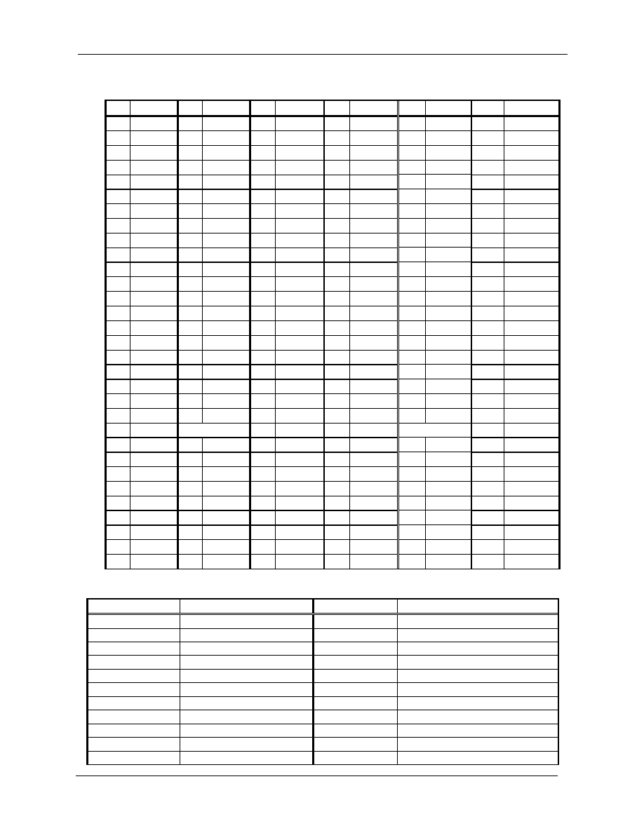
PIN ASSIGNMENT
*These pins should be NC in the system which does not support SPD
PIN
PIN DESCRIPTION
PIN
PIN DESCRIPTION
A0~A11
Address input
VDD
Power supply(2.5V)
BA0~BA1
Bank Select Address
VDDQ
Power supply for DQs(2.5V)
DQ0~DQ63
Data input/output
VREF
Power supply for reference
CB0~CB7
Check Bit
VDDSPD
Serial EEPROM Power supply(3.3)
DQS0~DQS8
Data Strobe input/output
VSS
Ground
DM0~DM8
Data-in Mask
SA0~SA2
Address in EEPROM
CK0~/CK0
Clock input
SDA
Serial data I/O
CKE0~CKE1
Clock enable input
SCL
Serial clock
/CS0~/CS1
Chip Select input
VDDID
VDD identification flag
/RAS
Row Address strobe
NC
No connection
/CAS
Column Address strobe
PIN
Front
PIN
Back
PIN
Frontl
PIN
Back
PIN
Front
PIN
Back
1
VREF
32
A5
62
V
DDQ
93
V
SS
124
V
SS
154
/RAS
2
DQ0
33
DQ24
63
/WE
94
DQ4
125
A6
155
DQ45
3
V
SS
34
V
SS
64
DQ41
95
DQ5
126
DQ28
156
V
DDQ
4
DQ1
35
DQ25
65
/CAS
96
V
DDQ
127
DQ29
157
/CS0
5
DQS0
36
DQS3
66
V
SS
97
DM0
128
V
DDQ
158
/CS1
6
DQ2
37
A4
67
DQS5
98
DQ6
129
DM3
159
DM5
7
V
DD
38
V
DD
68
DQ42
99
DQ7
130
A3
160
V
SS
8
DQ3
39
DQ26
69
DQ43
100
V
SS
131
DQ30
161
DQ46
9
NC
40
DQ27
70
V
DD
101
NC
132
V
SS
162
DQ47
10
/RESET
41
A2
71
* /CS2
102
NC
133
DQ31
163
* /CS3
11
V
SS
42
V
SS
72
DQ48
103
*A13
134
CB4
164
V
DDQ
12
DQ8
43
A1
73
DQ49
104
V
DDQ
135
CB5
165
DQ52
13
DQ9
44
CB0
74
V
SS
105
DQ12
136
V
DDQ
166
DQ53
14
DQS1
45
CB1
75
* CK2
106
DQ13
137
CK0
167
NC
15
V
DDQ
46
V
DD
76
* /CK2
107
DM1
138
/CK0
168
V
DD
16
* CK1
47
DQS8
77
V
DDQ
108
V
DD
139
V
SS
169
DM6
17
* /CK1
48
A0
78
DQS6
109
DQ14
140
DM8
170
DQ54
18
V
SS
49
CB2
79
DQ50
110
DQ15
141
A10
171
DQ55
19
DQ10
50
V
SS
80
DQ51
111
CKE1
142
CB6
172
V
DDQ
20
DQ11
51
CB3
81
V
SS
112
V
DDQ
143
V
DDQ
173
NC
21
CKE0
52
BA1
82
VDDID
113
* BA2
144
CB7
174
DQ60
22
V
DDQ
KEY
83
DQ56
114
DQ20
KEY
175
DQ61
23
DQ16
53
DQ32
84
DQ57
115
*A12
145
V
SS
176
V
SS
24
DQ17
54
V
DDQ
85
V
DD
116
V
SS
146
DQ36
177
DM7
25
DQS2
55
DQ33
86
DQS7
117
DQ21
147
DQ37
178
DQ62
26
V
SS
56
DQS4
87
DQ58
118
A11
148
V
DD
179
DQ63
27
A9
57
DQ34
88
DQ59
119
DM2
149
DM4
180
V
DDQ
28
DQ18
58
V
SS
89
V
SS
120
V
DD
150
DQ38
181
SA0
29
A7
59
BA0
90
NC
121
DQ22
151
DQ39
182
SA1
30
V
DDQ
60
DQ35
91
SDA
122
A8
152
V
SS
183
SA2
31
DQ19
61
DQ40
92
SCL
123
DQ23
153
DQ44
184
VDDSPD

HANBit HDD32M72B18RPW
URL : www.hbe.co.kr 3 HANBit Electronics Co.,Ltd.
REV 1.0 (August.2002)
FUNCTIONAL BLOCK DIAGRAM
/RCS0
/RCS1
Notes:
1. DQ-to-I/O wiring may be changed within a byte.
2. DQ/DQS/DM/CKE/S relationships must be
maintained as shown.
3. DQ/DQS resistors should be 22 Ohms.
4. VDDID strap connections
(for memory device VDD, VDDQ):
STRAP OUT (OPEN): VDD = VDDQ
STRAP IN (VSS): VDD
VDDQ.
5. RS0 and RS1 alternate between the back and front
sides of the DIMM.
6.Address and control resistors should be 22 Ohms.
/RCS1
/RCS0
A0~A11
RA0~RA11 A0~A1
1

HANBit HDD32M72B18RPW
URL : www.hbe.co.kr 4 HANBit Electronics Co.,Ltd.
REV 1.0 (August.2002)
PIN FUNCTION DESCRIPTION
Pin
Name
Input Function
CK, /CK
Clock
CK and CK are differential clock inputs. All address and control input signals are
sam-pled on the positive edge of CK and negative edge of CK. Output (read) data
is referenced to both edges of CK. Internal clock signals are derived from CK/CK.
CKE
Clock Enable
CKE HIGH activates, and CKE LOW deactivates internal clock signals, and device
input buffers and output drivers. Deactivating the clock provides PRECHARGE
POWER-DOWN and SELF REFRESH operation (all banks idle), or ACTIVE
POWER-DOWN(row ACTIVE in any bank). CKE is synchronous for all functions
except for disabling outputs, which is achieved asynchronously. Input buffers,
excluding CK, CK and CKE are disabled during power-down and self refresh
modes, providing low standby power. CKE will recognizean LVCMOS LOW level
prior to VREF being stable on power-up.
/CS
Chip Select
CS enables(registered LOW) and disables(registered HIGH) the command
decoder.
All commands are masked when CS is registered HIGH. CS provides for external
bank selection on systems with multiple banks. CS is considered part of the
command code.
A0 ~ A11
Address
Row/column addresses are multiplexed on the same pins.
Row address : RA0 ~ RA11, Column address : CA0 ~ CA9
BA0 ~ BA1
Bank select address
BA0 and BA1 define to which bank an ACTIVE, READ, WRITE or PRE-CHARGE
command is being applied.
/RAS
Row address strobe
Latches row addresses on the positive going edge of the CLK with /RAS low.
Enables row access & precharge.
/CAS
Column
address
strobe
Latches column addresses on the positive going edge of the CLK with /CAS low.
Enables column access.
/WE
Write enable
Enables write operation and row precharge.
Latches data in starting from /CAS, /WE active.
DQS0~8
Data Strobe
Output with read data, input with write data. Edge-aligned with read data, cen-
tered in write data. Used to capture write data.
DM0~8
Input Data Mask
DM is an input mask signal for write data. Input data is masked when DM is
sampled HIGH along with that input data during a WRITE access. DM is sampled
on both edges of DQS. DM pins include dummy loading internally, to matches the
DQ and DQS load-ing.
DQ0 ~ 63
Data input/output
Data inputs/outputs are multiplexed on the same pins.
CB0~CB7
Check Bit
Check Bit Input/Output pins
VDDQ
Supply
DQ Power Supply : +2.5V
±
0.2V.
VDD
Supply
Power Supply : +2.5V
±
0.2V (device specific).
VSS
Supply
DQ Ground.
VREF
Supply
SSTL_2 reference voltage.
VDDSPD
Supply
Serial EEPROM Power Supply : 3.3v
VDDID
VDD identification Flag

HANBit HDD32M72B18RPW
URL : www.hbe.co.kr 5 HANBit Electronics Co.,Ltd.
REV 1.0 (August.2002)
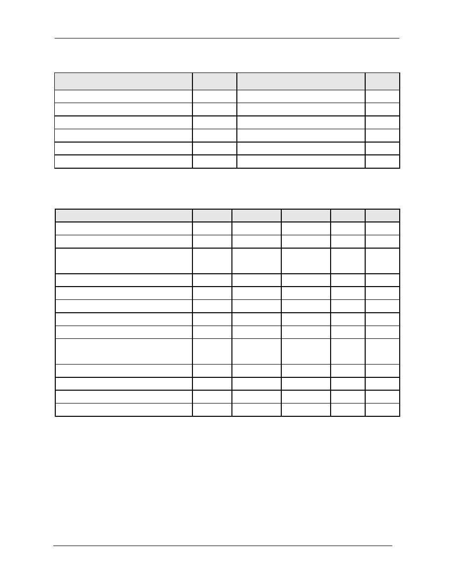
ABSOLUTE MAXIMUM RATINGS
PARAMETER
SYMBOL
RATING
UNTE
Voltage on any pin relative to Vss
V
IN
, V
OUT
-0.5 ~ 3.6
V
Voltage on V
DD
supply relative to Vss
V
DD
-1.0 ~ 3.6
V
Voltage on V
DDQ
supply relative to Vss
V
DDQ
-0.5 ~ 3.6
V
Storage temperature
T
STG
-55 ~ +150
∞
C
Power dissipation
P
D
18
W
Short circuit current
I
OS
50
mA
Notes: Operation at above absolute maximum rating can adversely affect device reliability
DC OPERATING CONDITIONS
(Recommended operating conditions (Voltage referenced to Vss = 0V, T
A
= 0 to 70
∞
C) )
PARAMETER
SYMBOL
MIN
MAX
UNIT
NOTE
Supply Voltage
V
DD
2.3
2.7
V
I/O Supply Voltage
V
DDQ
2.3
2.7
V
I/O Reference Voltage
V
REF
V
DDQ
/2 - 50mA
V
DDQ
/2 +
50mA
V
1
I/O Termination Voltage(system)
V
TT
V
REF
≠
0.04
V
REF
+ 0.04
V
2
Input High Voltage
V
IH
(DC)
V
REF
+ 0.15
V
REF
+ 0.3
V
4
Input Low Voltage
V
IL
(DC)
-0.3
V
REF
- 0.15
V
4
Input Voltage Level, CK and /CK inputs
V
IN
(DC)
-0.3
V
DDQ
+ 0.3
V
Input Differential Voltage, CK and /CK inputs
V
ID
(DC)
0.3
V
DDQ
+ 0.6
V
3
Input crossing point Voltage, CK and /CK
inputs
V
IX
(DC)
1.15
1.35
V
5
Input leakage current
I
LI
-2
2
uA
Output leakage current
I
OZ
-5
5
uA
Output High current (V
OUT
= 1.95V)
I
OH
-16.8
mA
Output Low current (V
OUT
= 0.35V)
I
OL
16.8
mA
Notes :
1. Includes
±
25mV margin for DC offset on V
REF
, and a combined total of
±
50mV margin for all AC noise and DC
offset on V
REF
, bandwidth limited to 20MHz. The DRAM must accommodate DRAM current spikes on V
REF
and
internal DRAM noise coupled to V
REF
, both of which may result in V
REF
noise. V
REF
should be de-coupled with an
inductance of
3nH.
2. V
TT
is not applied directly to the device. V
TT
is a system supply for signal termination resistors, is expected to be set
equal to V
REF
, and must track variations in the DC level of V
REF
3. V
ID
is the magnitude of the difference between the input level on CK and the input level on CK.
4. These parameters should be tested at the pin on actual components and may be checked at either the pin or the
pad in simulation. The AC and DC input specifications are relative to a V
REF
envelop that has been bandwidth limited
to 200MHZ.
5. The value of V
IX
is expected to equal 0.5*VDDQ of the transmitting device and must track variations in the dc level of
the same.
6. These charactericteristics obey the SSTL-2 class II standards.


