 | –≠–ª–µ–∫—Ç—Ä–æ–Ω–Ω—ã–π –∫–æ–º–ø–æ–Ω–µ–Ω—Ç: 82C37 | –°–∫–∞—á–∞—Ç—å:  PDF PDF  ZIP ZIP |
S E M I C O N D U C T O R
4-192
March 1997
82C37A
CMOS High Performance
Programmable DMA Controller
Features
∑ Compatible with the NMOS 8237A
∑ Four Independent Maskable Channels with Autoinitial-
ization Capability
∑ Cascadable to any Number of Channels
∑ High Speed Data Transfers:
- Up to 4MBytes/sec with 8MHz Clock
- Up to 6.25MBytes/sec with 12.5MHz Clock
∑ Memory-to-Memory Transfers
∑ Static CMOS Design Permits Low Power Operation
- ICCSB = 10
µ
A Maximum
- ICCOP = 2mA/MHz Maximum
∑ Fully TTL/CMOS Compatible
∑ Internal Registers may be Read from Software
Description
The 82C37A is an enhanced version of the industry standard
8237A Direct Memory Access (DMA) controller, fabricated
using Harris' advanced 2 micron CMOS process. Pin
compatible with NMOS designs, the 82C37A offers
increased functionality, improved performance, and
dramatically reduced power consumption. The fully static
design permits gated clock operation for even further
reduction of power.
The 82C37A controller can improve system performance by
allowing external devices to transfer data directly to or from
system memory. Memory-to-memory transfer capability is
also provided, along with a memory block initialization fea-
ture. DMA requests may be generated by either hardware or
software, and each channel is independently programmable
with a variety of features for flexible operation.
The 82C37A is designed to be used with an external
address latch, such as the 82C82, to demultiplex the most
significant 8-bits of address. The 82C37A can be used with
industry standard microprocessors such as 80C286, 80286,
80C86, 80C88, 8086, 8088, 8085, Z80, NSC800, 80186 and
others. Multimode programmability allows the user to select
from three basic types of DMA services, and reconfiguration
under program control is possible even with the clock to the
controller stopped. Each channel has a full 64K address and
word count range, and may be programmed to autoinitialize
these registers following DMA termination (end of process).
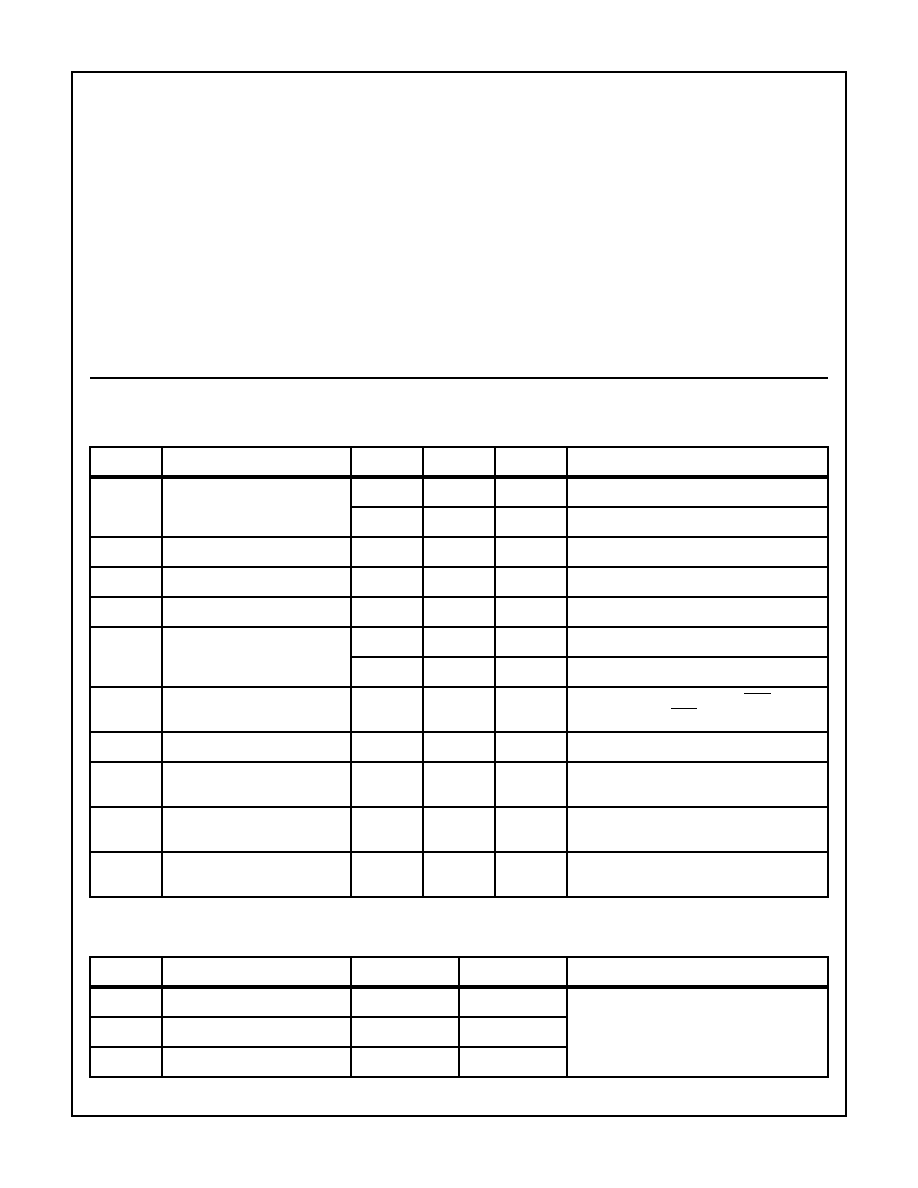
Ordering Information
PART NUMBER
PACKAGE
TEMPERATURE
RANGE
PKG. NO.
5MHz
8MHz
12.5MHz
CP82C37A-5
CP82C37A
CP82C37A-12
40 Ld PDIP
0
o
C to +70
o
C
E40.6
IP82C37A-5
IP82C37A
IP82C37A-12
-40
o
C to +85
o
C
E40.6
CS82C37A-5
CS82C37A
CS82C37A-12
44 Ld PLCC
0
o
C to +70
o
C
N44.65
IS82C37A-5
IS82C37A
IS82C37A-12
-40
o
C to +85
o
C
N44.65
CD82C37A-5
CD82C37A
CD82C37A-12
40 Ld CERDIP
0
o
C to +70
o
C
F40.6
ID82C37A-5
ID82C37A
ID82C37A-12
-40
o
C to +85
o
C
F40.6
MD82C37A-5/B
MD82C37A/B
MD82C37A-12/B
-55
o
C to +125
o
C
F40.6
5962-9054301MQA
5962-9054302MQA
5962-9054303MQA
SMD#
F40.6
MR82C37A-5/B
MR82C37A/B
MR82C37A-12/B
44 Pad CLCC
-55
o
C to +125
o
C
J44.A
5962-9054301MXA
5962-9054302MXA
5962-9054303MXA
SMD#
J44.A
CAUTION: These devices are sensitive to electrostatic discharge. Users should follow proper IC Handling Procedures.
Copyright
©
Harris Corporation 1997
File Number
2967.1
4-193
82C37A
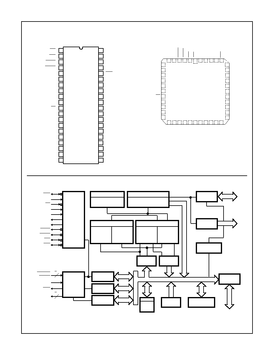
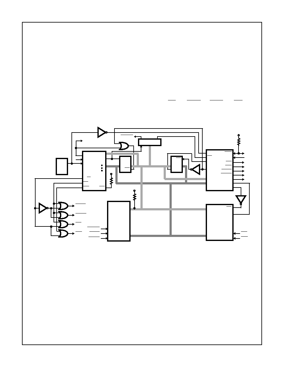
Block Diagram
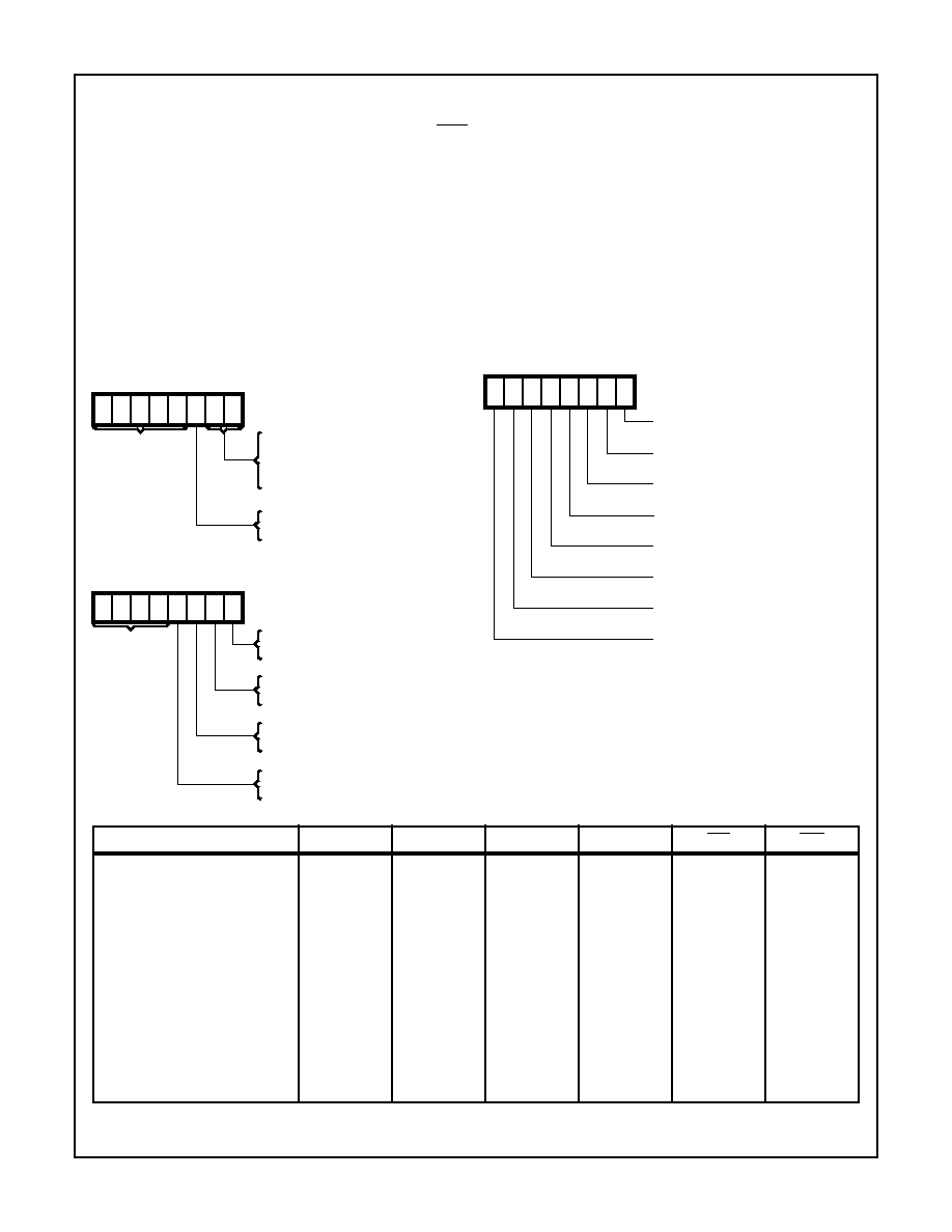
Pinouts
82C37A (PDIP/CERDIP)
TOP VIEW
82C37A (CLCC/PLCC)
TOP VIEW
13
1
2
3
4
5
6
7
8
9
10
11
12
14
15
16
17
18
19
20
IOR
IOW
MEMR
MEMW
NC
READY
HLDA
ADSTB
AEN
HRQ
CS
CLK
RESET
DACK2
DACK3
DREQ3
DREQ2
DREQ1
DREQ0
(GND) VSS
28
40
39
38
37
36
35
34
33
32
31
30
29
27
26
25
24
23
22
21
A7
A6
A5
A4
EOP
A3
A2
A1
A0
VCC
DB0
DB1
DB2
DB3
DB4
DACK0
DACK1
DB5
DB6
DB7
14
13
12
11
10
9
8
7
17
16
15
2
5
30
35
39
38
37
36
33
34
32
31
29
4
6
3
1
40
41
42
43
44
28
27
26
25
24
23
22
21
20
19
18
CS
DACK2
NC
NC
CLK
HRQ
NC
A3
A2
A1
A0
VCC
DB0
DB1
DB2
DB3
NC
DB4
READ
Y
NC
A7
A6
A5
MEMW
A4
EOP
D
A
CK3
DREQ3
DREQ2
DREQ1
DREQ0
GND
DB5
D
A
CK1
DB7
D
A
CK0
DB6
MEMR
ADSTB
AEN
IO
W
RESET
HLDA
IOR
A4 - A7
EOP
RESET
CS
READY
CLK
AEN
ADSTB
MEMR
MEMW
IOR
IOW
TIMING
AND
CONTROL
DREQ0 -
HLDA
HRQ
DACK0 -
PRIORITY
ENCODER
AND
ROTATING
PRIORITY
LOGIC
DACK3
4
DREQ3
4
COMMAND
(8)
MASK
(4)
REQUEST
(4)
MODE
(4 x 6)
STATUS
(8)
TEMPORARY
(8)
INTERNAL DATA BUS
DECREMENTOR
COUNT REG (16)
TEMP WORD
INC/DECREMENTOR
REG (16)
TEMP ADDRESS
BUFFER
IO
16-BIT BUS
READ BUFFER
ADDRESS
BASE
(16)
WORD
BASE
COUNT
(16)
READ WRITE BUFFER
ADDRESS
CURRENT
(16)
WORD
CURRENT
COUNT
(16)
16-BIT BUS
BUFFER
WRITE
BUFFER
READ
A8 - A15
BUFFER
OUTPUT
CONTROL
COMMAND
D0 - D1
A0 - A3
BUFFER
IO
DB0 - DB7
4-194
82C37A
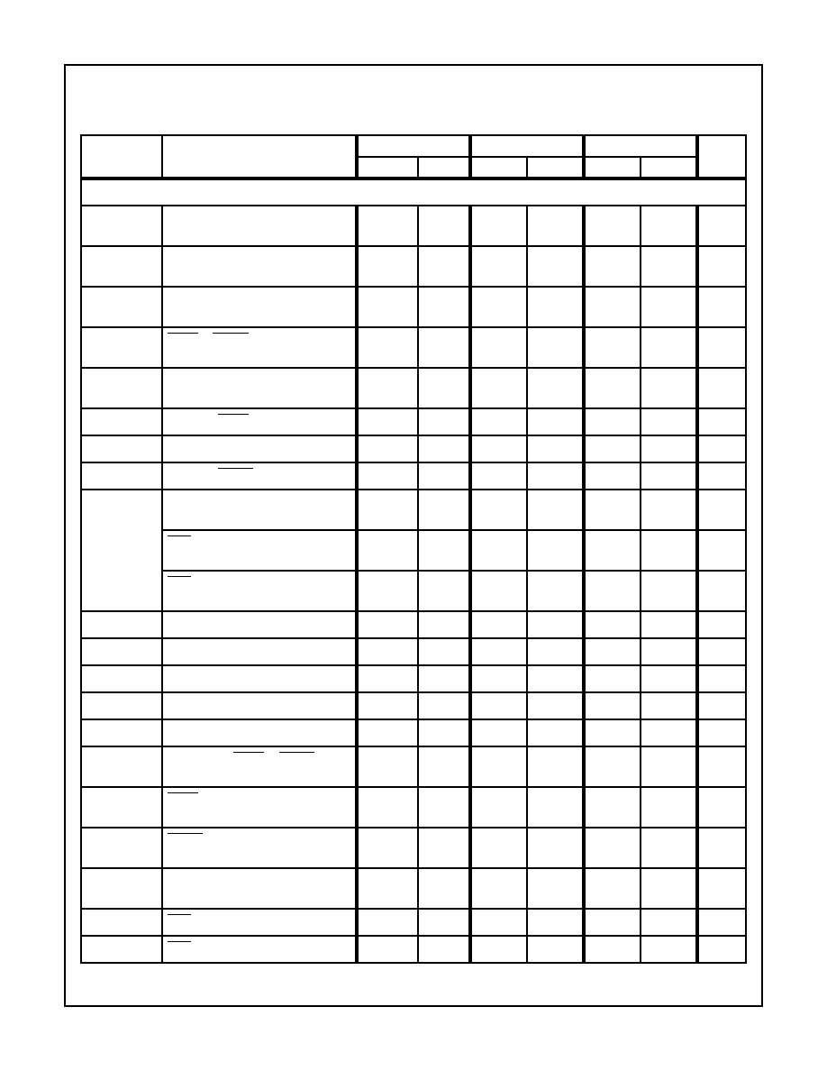
Pin Description
SYMBOL
PIN
NUMBER
TYPE
DESCRIPTION
V
CC
31
V
CC
: is the +5V power supply pin. A 0.1
µ
F capacitor between pins 31 and 20 is recommended for
decoupling.
GND
20
Ground
CLK
12
I
CLOCK INPUT: The Clock Input is used to generate the timing signals which control 82C37A
operations. This input may be driven from DC to 12.5MHz for the 82C37A-12, from DC to 8MHz for
the 82C37A, or from DC to 5MHz for the 82C37A-5. The Clock may be stopped in either state for
standby operation.
CS
11
I
CHIP SELECT: Chip Select is an active low input used to enable the controller onto the data bus for
CPU communications.
RESET
13
I
RESET: This is an active high input which clears the Command, Status, Request, and Temporary
registers, the First/Last Flip-Flop, and the mode register counter. The Mask register is set to ignore
requests. Following a Reset, the controller is in an idle cycle.
READY
6
I
READY: This signal can be used to extend the memory read and write pulses from the 82C37A to
accommodate slow memories or I/O devices. READY must not make transitions during its specified
set-up and hold times. See Figure 12 for timing. READY is ignored in verify transfer mode.
HLDA
7
I
HOLD ACKNOWLEDGE: The active high Hold Acknowledge from the CPU indicates that it has
relinquished control of the system busses. HLDA is a synchronous input and must not transition
during its specified set-up time. There is an implied hold time (HLDA inactive) of TCH from the rising
edge of CLK, during which time HLDA must not transition.
DREQ0-
DREQ3
16-19
I
DMA REQUEST: The DMA Request (DREQ) lines are individual asynchronous channel request
inputs used by peripheral circuits to obtain DMA service. In Fixed Priority, DREQ0 has the highest
priority and DREQ3 has the lowest priority. A request is generated by activating the DREQ line of a
channel. DACK will acknowledge the recognition of a DREQ signal. Polarity of DREQ is
programmable. RESET initializes these lines to active high. DREQ must be maintained until the
corresponding DACK goes active. DREQ will not be recognized while the clock is stopped. Unused
DREQ inputs should be pulled High or Low (inactive) and the corresponding mask bit set.
DB0-DB7
21-23
26-30
I/O
DATA BUS: The Data Bus lines are bidirectional three-state signals connected to the system data
bus. The outputs are enabled in the Program condition during the I/O Read to output the contents
of a register to the CPU. The outputs are disabled and the inputs are read during an I/O Write cycle
when the CPU is programming the 82C37A control registers. During DMA cycles, the most signifi-
cant 8-bits of the address are output onto the data bus to be strobed into an external latch by ADSTB.
In memory-to-memory operations, data from the memory enters the 82C37A on the data bus during
the read-from-memory transfer, then during the write-to-memory transfer, the data bus outputs write
the data into the new memory location.
IOR
1
I/O
I/O READ: I/O Read is a bidirectional active low three-state line. In the Idle cycle, it is an input con-
trol signal used by the CPU to read the control registers. In the Active cycle, it is an output control
signal used by the 82C37A to access data from the peripheral during a DMA Write transfer.
IOW
2
I/O
I/O WRITE: I/O Write is a bidirectional active low three-state line. In the Idle cycle, it is an input con-
trol signal used by the CPU to load information into the 82C37A. In the Active cycle, it is an output
control signal used by the 82C37A to load data to the peripheral during a DMA Read transfer.
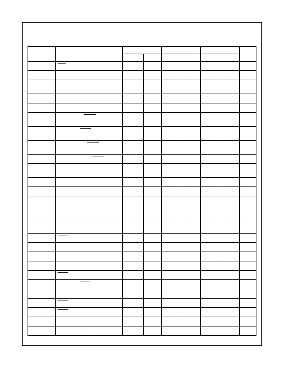
4-195
82C37A
EOP
36
I/O
END OF PROCESS: End of Process (EOP) is an active low bidirectional signal. Information
concerning the completion of DMA services is available at the bidirectional EOP pin.
The 82C37A allows an external signal to terminate an active DMA service by pulling the EOP pin
low. A pulse is generated by the 82C37A when terminal count (TC) for any channel is reached,
except for channel 0 in memory-to-memory mode. During memory-to-memory transfers, EOP will
be output when the TC for channel 1 occurs.
The EOP pin is driven by an open drain transistor on-chip, and requires an external pull-up resistor
to V
CC
.
When an EOP pulse occurs, whether internally or externally generated, the 82C37A will terminate
the service, and if autoinitialize is enabled, the base registers will be written to the current registers
of that channel. The mask bit and TC bit in the status word will be set for the currently active channel
by EOP unless the channel is programmed for autoinitialize. In that case, the mask bit remains clear.
A0-A3
32-35
I/O
ADDRESS: The four least significant address lines are bidirectional three-state signals. In the Idle
cycle, they are inputs and are used by the 82C37A to address the control register to be loaded or
read. In the Active cycle, they are outputs and provide the lower 4-bits of the output address.
A4-A7
37-40
O
ADDRESS: The four most significant address lines are three-state outputs and provide 4-bits of
address. These lines are enabled only during the DMA service.
HRQ
10
O
HOLD REQUEST: The Hold Request (HRQ) output is used to request control of the system bus.
When a DREQ occurs and the corresponding mask bit is clear, or a software DMA request is made,
the 82C37A issues HRQ. The HLDA signal then informs the controller when access to the system
busses is permitted. For stand-alone operation where the 82C37A always controls the busses, HRQ
may be tied to HLDA. This will result in one S0 state before the transfer.
DACK0-
DACK3
14, 15
24, 25
O
DMA ACKNOWLEDGE: DMA acknowledge is used to notify the individual peripherals when one
has been granted a DMA cycle. The sense of these lines is programmable. RESET initializes them
to active low.
AEN
9
O
ADDRESS ENABLE: Address Enable enables the 8-bit latch containing the upper 8 address bits
onto the system address bus. AEN can also be used to disable other system bus drivers during DMA
transfers. AEN is active high.
ADSTB
8
O
ADDRESS STROBE: This is an active high signal used to control latching of the upper address
byte. It will drive directly the strobe input of external transparent octal latches, such as the 82C82.
During block operations, ADSTB will only be issued when the upper address byte must be updated,
thus speeding operation through elimination of S1 states. ADSTB timing is referenced to the falling
edge of the 82C37A clock.
MEMR
3
O
MEMORY READ: The Memory Read signal is an active low three-state output used to access data
from the selected memory location during a DMA Read or a memory-to-memory transfer.
MEMW
4
O
MEMORY WRITE: The Memory Write signal is an active low three-state output used to write data
to the selected memory location during a DMA Write or a memory-to-memory transfer.
NC
5
NO CONNECT: Pin 5 is open and should not be tested for continuity.
Pin Description
(Continued)
SYMBOL
PIN
NUMBER
TYPE
DESCRIPTION
4-196
82C37A
Functional Description
The 82C37A direct memory access controller is designed to
improve the data transfer rate in systems which must
transfer data from an I/O device to memory, or move a block
of memory to an I/O device. It will also perform memory-to-
memory block moves, or fill a block of memory with data
from a single location. Operating modes are provided to
handle single byte transfers as well as discontinuous data
streams, which allows the 82C37A to control data movement
with software transparency.
The DMA controller is a state-driven address and control
signal generator, which permits data to be transferred
directly from an I/O device to memory or vice versa without
ever being stored in a temporary register. This can greatly
increase the data transfer rate for sequential operations,
compared with processor move or repeated string
instructions. Memory-to-memory operations require
temporary internal storage of the data byte between
generation of the source and destination addresses, so
memory-to-memory transfers take place at less than half the
rate of I/O operations, but still much faster than with central
processor techniques. The maximum data transfer rates
obtainable with the 82C37A are shown in Figure 1.
The block diagram of the 82C37A is shown on page 2. The
timing and control block, priority block, and internal registers
are the main components. Figure 2 lists the name and size
of the internal registers. The timing and control block derives
internal timing from clock input, and generates external
control signals. The Priority Encoder block resolves priority
contention between DMA channels requesting service
simultaneously.
DMA Operation
In a system, the 82C37A address and control outputs and
data bus pins are basically connected in parallel with the
system busses. An external latch is required for the upper
address byte. While inactive, the controller's outputs are in a
high impedance state. When activated by a DMA request
and bus control is relinquished by the host, the 82C37A
drives the busses and generates the control signals to
perform the data transfer. The operation performed by
activating one of the four DMA request inputs has previously
been programmed into the controller via the Command,
Mode, Address, and Word Count registers.
For example, if a block of data is to be transferred from RAM
to an I/O device, the starting address of the data is loaded
into the 82C37A Current and Base Address registers for a
particular channel, and the length of the block is loaded into
the channel's Word Count register. The corresponding Mode
register is programmed for a memory-to-I/O operation (read
transfer), and various options are selected by the Command
register and the other Mode register bits. The channel's
mask bit is cleared to enable recognition of a DMA request
(DREQ). The DREQ can either be a hardware signal or a
software command.
Once initiated, the block DMA transfer will proceed as the
controller outputs the data address, simultaneous MEMR
and IOW pulses, and selects an I/O device via the DMA
acknowledge (DACK) outputs. The data byte flows directly
from the RAM to the I/O device. After each byte is
transferred, the address is automatically incremented (or
decremented) and the word count is decremented. The
operation is then repeated for the next byte. The controller
stops transferring data when the Word Count register
underflows, or an external EOP is applied.
To further understand 82C37A operation, the states
generated by each clock cycle must be considered. The
DMA controller operates in two major cycles, active and idle.
After being programmed, the controller is normally idle until
a DMA request occurs on an unmasked channel, or a
software request is given. The 82C37A will then request
control of the system busses and enter the active cycle. The
active cycle is composed of several internal states,
depending on what options have been selected and what
type of operation has been requested.
82C37A
TRANSFER
TYPE
5MHz
8MHz
12.5MHz
UNIT
Compressed
2.50
4.00
6.25
MByte/sec
Normal I/O
1.67
2.67
4.17
MByte/sec
Memory-to-
Memory
0.63
1.00
1.56
MByte/sec
FIGURE 1. DMA TRANSFER RATES
NAME
SIZE
NUMBER
Base Address Registers
16-Bits
4
Base Word Count Registers
16-Bits
4
Current Address Registers
16-Bits
4
Current Word Count Registers
16-Bits
4
Temporary Address Register
16-Bits
1
Temporary Word Count Register
16-Bits
1
Status Register
8-Bits
1
Command Register
8-Bits
1
Temporary Register
8-Bits
1
Mode Registers
6-Bits
4
Mask Register
4-Bits
1
Request Register
4-Bits
1
FIGURE 2. 82C37A INTERNAL REGISTERS

4-197
82C37A
The 82C37A can assume seven separate states, each
composed of one full clock period. State I (SI) is the idle
state. It is entered when the 82C37A has no valid DMA
requests pending, at the end of a transfer sequence, or
when a Reset or Master Clear has occurred. While in SI, the
DMA controller is inactive but may be in the Program
Condition (being programmed by the processor).
State 0 (S0) is the first state of a DMA service. The 82C37A
has requested a hold but the processor has not yet returned
an acknowledge. The 82C37A may still be programmed until
it has received HLDA from the CPU. An acknowledge from
the CPU will signal the DMA transfer may begin. S1, S2, S3,
and S4 are the working state of the DMA service. If more
time is needed to complete a transfer than is available with
normal timing, wait states (SW) can be inserted between S3
and S4 in normal transfers by the use of the Ready line on
the 82C37A. For compressed transfers, wait states can be
inserted between S2 and S4. See timing Figures 14 and 15.
Note that the data is transferred directly from the I/O device
to memory (or vice versa) with IOR and MEMW (or MEMR
and IOW) being active at the same time. The data is not read
into or driven out of the 82C37A in I/O-to-memory or
memory-to-I/O DMA transfers.
Memory-to-memory transfers require a read-from and a write-
to memory to complete each transfer. The states, which
resemble the normal working states, use two-digit numbers
for identification. Eight states are required for a single transfer.
The first four states (S11, S12, S13, S14) are used for the
read-from-memory half and the last four state (S21, S22, S23,
S24) for the write-to-memory half of the transfer.
Idle Cycle
When no channel is requesting service, the 82C37A will
enter the idle cycle and perform "SI" states. In this cycle, the
82C37A will sample the DREQ lines on the falling edge of
every clock cycle to determine if any channel is requesting a
DMA service.
Note that for standby operation where the clock has been
stopped, DMA requests will be ignored. The device will
respond to CS (chip select), in case of an attempt by the
microprocessor to write or read the internal registers of the
82C37A. When CS is low and HLDA is low, the 82C37A
enters the Program Condition. The CPU can now establish,
change or inspect the internal definition of the part by read-
ing from or writing to the internal registers.
The 82C37A may be programmed with the clock stopped, pro-
vided that HLDA is low and at least one rising clock edge has
occurred after HLDA was driven low, so the controller is in an SI
state. Address lines A0-A3 are inputs to the device and select
which registers will be read or written. The IOR and IOW lines
are used to select and time the read or write operations. Due to
the number and size of the internal registers, an internal flip-flop
called the First/Last Flip-Flop is used to generate an additional
bit of address. The bit is used to determine the upper or lower
byte of the 16-bit Address and Work Count registers. The flip-
flop is reset by Master Clear or RESET. Separate software
commands can also set or reset this flip-flop.
Special software commands can be executed by the
82C37A in the Program Condition. These commands are
decoded as sets of addresses with CS, IOR, and IOW. The
commands do not make use of the data bus. Instructions
include Set and Clear First/Last Flip-Flop, Master Clear,
Clear Mode Register Counter, and Clear Mask Register.
Active Cycle
When the 82C37A is in the Idle cycle, and a software
request or an unmasked channel requests a DMA service,
the device will issue HRQ to the microprocessor and enter
the Active cycle. It is in this cycle that the DMA service will
take place, in one of four modes:
Single Transfer Mode - In Single Transfer mode, the device
is programmed to make one transfer only. The word count
will be decremented and the address decremented or
incremented following each transfer. When the word count
"rolls over" from zero to FFFFH, a terminal count bit in the
status register is set, an EOP pulse is generated, and the
channel will autoinitialize if this option has been selected. If
not programmed to autoinitialize, the mask bit will be set,
along with the TC bit and EOP pulse.
DREQ must be held active until DACK becomes active. If
DREQ is held active throughout the single transfer, HRQ will
go inactive and release the bus to the system. It will again go
active and, upon receipt of a new HLDA, another single
transfer will be performed, unless a higher priority channel
takes over. In 8080A, 8085A, 80C88, or 80C86 systems, this
will ensure one full machine cycle execution between DMA
transfers. Details of timing between the 82C37A and other
bus control protocols will depend upon the characteristics of
the microprocessor involved.
Block Transfer Mode - In Block Transfer mode, the device
is activated by DREQ or software request and continues
making transfers during the service until a TC, caused by
word count going to FFFFH, or an external End of Process
(EOP) is encountered. DREQ need only be held active until
DACK becomes active. Again, an Autoinitialization will occur
at the end of the service if the channel has been
programmed for that option.
Demand Transfer Mode - In Demand Transfer mode the
device continues making transfers until a TC or external EOP is
encountered, or until DREQ goes inactive. Thus, transfer may
continue until the I/O device has exhausted its data capacity.
After the I/O device has had a chance to catch up, the DMA
service is reestablished by means of a DREQ. During the time
between services when the microprocessor is allowed to oper-
ate, the intermediate values of address and word count are
stored in the 82C37A Current Address and Current Word
Count registers. Higher priority channels may intervene in the
demand process, once DREQ has gone inactive. Only an EOP
can cause an Autoinitialization at the end of service. EOP is
generated either by TC or by an external signal.
Cascade Mode - This mode is used to cascade more than
one 82C37A for simple system expansion. The HRQ and
HLDA signals from the additional 82C37A are connected to
the DREQ and DACK signals respectively of a channel for
4-198
82C37A
the initial 82C37A.This allows the DMA requests of the
additional device to propagate through the priority network
circuitry of the preceding device. The priority chain is
preserved and the new device must wait for its turn to
acknowledge requests. Since the cascade channel of the
initial 82C37A is used only for prioritizing the additional
device, it does not output an address or control signals of its
own. These could conflict with the outputs of the active chan-
nel in the added device. The initial 82C37A will respond to
DREQ and generate DACK but all other outputs except HRQ
will be disabled. An external EOP will be ignored by the initial
device, but will have the usual effect on the added device.
Figure 3 shows two additional devices cascaded with an
initial device using two of the initial device's channels. This
forms a two-level DMA system. More 82C37As could be
added at the second level by using the remaining channels
of the first level. Additional devices can also be added by
cascading into the channels of the second level devices,
forming a third level.
When programming cascaded controllers, start with the first
level device (closest to the microprocessor). After RESET,
the DACK outputs are programmed to be active low and are
held in the high state. If they are used to drive HLDA directly,
the second level device(s) cannot be programmed until
DACK polarity is selected as active high on the initial device.
Also, the initial device's mask bits function normally on
cascaded channels, so they may be used to inhibit second-
level services.
Transfer Types
Each of the three active transfer modes can perform three dif-
ferent types of transfers. These are Read, Write and Verify.
Write transfers move data from an I/O device to the memory
by activating MEMW and IOR. Read transfers move data from
memory to an I/O device by activating MEMR and IOW.
Verify transfers are pseudo-transfers. The 82C37A operates
as in Read or Write transfers generating addresses and
responding to EOP, etc., however the memory and I/O
control lines all remain inactive. Verify mode is not permitted
for memory-to-memory operation. READY is ignored during
Verify transfers.
Autoinitialize - By setting bit 4 in the Mode register, a
channel may be set up as an Autoinitialize channel. During
Autoinitialization, the original values of the Current Address
and Current Word Count registers are automatically restored
from the Base Address and Base Word Count registers of
the channel following EOP. The base registers are loaded
simultaneously with the current registers by the micropro-
cessor and remain unchanged throughout the DMA service.
The mask bit is not set when the channel is in Autoinitialize
mode. Following Autoinitialization, the channel is ready to
perform another DMA service, without CPU intervention, as
soon as a valid DREQ is detected, or software request
made.
Memory-to-Memory - To perform block moves of data from
one memory address space to another with minimum of
program effort and time, the 82C37A includes a memory-to-
memory transfer feature. Setting bit 0 in the Command
register selects channels 0 and 1 to operate as memory-to-
memory transfer channels.
The transfer is initiated by setting the software or hardware
DREQ for channel 0. The 82C37A requests a DMA service
in the normal manner. After HLDA is true, the device, using
four-state transfers in Block Transfer mode, reads data from
the memory. The channel 0 Current Address register is the
source for the address used and is decremented or
incremented in the normal manner. The data byte read from
the memory is stored in the 82C37A internal Temporary reg-
ister. Another four-state transfer moves the data to memory
using the address in channel one's Current Address register
and incrementing or decrementing it in the normal manner.
The channel 1 Current Word Count is decremented.
When the word count of channel 1 decrements to FFFFH, a
TC is generated causing an EOP output, terminating the
service, and setting the channel 1 TC bit in the Status
register. The channel 1 mask bit will also be set, unless the
channel 1 mode register is programmed for autoinitialization.
Channel 0 word count decrementing to FFFFH will not set
the channel 0 TC bit in the status register nor generate an
EOP, nor set the channel 0 mask bit in this mode. It will
cause an autoinitialization of channel 0, if that option has
been selected.
If full Autoinitialization for a memory-to-memory operation is
desired, the channel 0 and channel 1 word counts must be
set to equal values before the transfer begins. Otherwise, if
channel 0 underflows before channel 1, it will autoinitialize
and set the data source address back to the beginning of the
block. If the channel 1 word count underflows before channel
0, the memory-to-memory DMA service will terminate, and
channel 1 will autoinitialize but channel 0 will not.
In memory-to-memory mode, Channel 0 may be
programmed to retain the same address for all transfers.
This allows a single byte to be written to a block of memory.
This channel 0 address hold feature is selected by setting bit
1 in the Command register.
The 82C37A will respond to external EOP signals during
memory-to-memory transfers, but will only relinquish the
system busses after the transfer is complete (i.e. after an
80C86/88
MICRO-
PROCESSOR
HRQ
HLDA
DREQ
DACK
DREQ
DACK
1ST LEVEL
82C37A
HRQ
HLDA
82C37A
HRQ
HLDA
82C37A
ADDITIONAL
DEVICES
2ND LEVEL
INITIAL DEVICE
FIGURE 3. CASCADED 82C37As
4-199
82C37A
S24 state). It should be noted that an external EOP cannot
cause the channel 0 Address and Word Count registers to
autoinitialize, even if the Mode register is programmed for
autoinitialization. An external EOP will autoinitialize the
channel 1 registers, if so programmed. Data comparators in
block search schemes may use the EOP input to terminate
the service when a match is found. The timing of memory-to-
memory transfers is found in Figure 13. Memory-to-memory
operations can be detected as an active AEN with no DACK
outputs.
Priority - The 82C37A has two types of priority encoding
available as software selectable options. The first is Fixed
Priority which fixes the channels in priority order based upon
the descending value of their numbers. The channel with the
lowest priority is 3 followed by 2, 1 and the highest priority
channel, 0. After the recognition of any one channel for ser-
vice, the other channels are prevented from interfering with
the service until it is completed.
The second scheme is Rotating Priority. The last channel to
get service becomes the lowest priority channel with the
others rotating accordingly. The next lower channel from the
channel serviced has highest priority on the following
request. Priority rotates every time control of the system
busses is returned to the processor.
Rotating Priority
With Rotating Priority in a single chip DMA system, any
device requesting service is guaranteed to be recognized
after no more than three higher priority services have
occurred. This prevents any one channel from monopolizing
the system.
Regardless of which priority scheme is chosen, priority is
evaluated every time a HLDA is returned to the 82C37A.
Compressed Timing - In order to achieve even greater
throughput where system characteristics permit, the 82C37A
can compress the transfer time to two clock cycles. From
Figure 12 it can be seen that state S3 is used to extend the
access time of the read pulse. By removing state S3, the
read pulse width is made equal to the write pulse width and
a transfer consists only of state S2 to change the address
and state S4 to perform the read/write. S1 states will still
occur when A8-A15 need updating (see Address
Generation). Timing for compressed transfers is found in
Figure 15. EOP will output in S2 if compressed timing is
selected. Compressed timing is not allowed for memory-to-
memory transfers.
Address Generation - In order to reduce pin count, the
82C37A multiplexes the eight higher order address bits on
the data lines. State S1 is used to output the higher order
address bits to an external latch from which they may be
placed on the address bus. The falling edge of Address
Strobe (ADSTB) is used to load these bits from the data
lines to the latch. Address Enable (AEN) is used to enable
the bits onto the address bus through a three-state enable.
The lower order address bits are output by the 82C37A
directly. Lines A0-A7 should be connected to the address
bus. Figure 12 shows the time relationships between CLK,
AEN, ADSTB, DB0-DB7 and A0-A7.
During Block and Demand Transfer mode service, which
include multiple transfers, the addresses generated will be
sequential. For many transfers the data held in the external
address latch will remain the same. This data need only
change when a carry or borrow from A7 to A8 takes place in
the normal sequence of addresses. To save time and speed
transfers, the 82C37A executes S1 states only when
updating of A8-A15 in the latch is necessary. This means for
long services, S1 states and Address Strobes may occur
only once every 256 transfers, a savings of 255 clock cycles
for each 256 transfers.
Programming
The 82C37A will accept programming from the host
processor anytime that HLDA is inactive, and at least one
rising clock edge has occurred after HLDA went low. It is the
responsibility of the host to assure that programming and
HLDA are mutually exclusive.
Note that a problem can occur if a DMA request occurs on
an unmasked channel while the 82C37A is being pro-
grammed. For instance, the CPU may be starting to repro-
gram the two byte Address register of channel 1 when
channel 1 receives a DMA request. If the 82C37A is enabled
(bit 2 in the Command register is 0), and channel 1 is
unmasked, a DMA service will occur after only one byte of
the Address register has been reprogrammed. This condi-
tion can be avoided by disabling the controller (setting bit 2
in the Command register) or masking the channel before
programming any of its registers. Once the programming is
complete, the controller can be enabled/unmasked.
After power-up it is suggested that all internal locations be
loaded with some known value, even if some channels are
unused. This will aid in debugging.
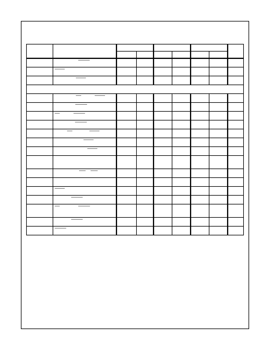
Register Description
Current Address Register - Each channel has a 16-bit
Current Address register. This register holds the value of the
address used during DMA transfers. The address is auto-
matically incremented or decremented by one after each
transfer and the values of the address are stored in the Cur-
rent Address register during the transfer. This register is writ-
ten or read by the microprocessor in successive 8-bit bytes.
See Figure 6 for programming information. It may also be
reinitialized by an Autoinitialize back to its original value.
Autoinitialize takes place only after an EOP. In memory-to-
memory mode, the channel 0 Current Address register can
be prevented from incrementing or decrementing by setting
the address hold bit in the Command register.
1st
SERVICE
0
1
2
3
Highest
Lowest
2nd
SERVICE
2
3
0
1
Service
3rd
SERVICE
3
0
1
2
Service
Request
Service
4-200
82C37A
Current Word Count Register - Each channel has a 16-bit
Current Word Count register. This register determines the
number of transfers to be performed. The actual number of
transfers will be one more than the number programmed in
the Current Word Count register (i.e., programming a count
of 100 will result in 101 transfers). The word count is
decremented after each transfer. When the value in the
register goes from zero to FFFFH, a TC will be generated.
This register is loaded or read in successive 8-bit bytes by
the microprocessor in the Program Condition. See Figure 6
for programming information. Following the end of a DMA
service it may also be reinitialized by an Autoinitialization
back to its original value. Autoinitialization can occur only
when an EOP occurs. If it is not Autoinitialized, this register
will have a count of FFFFH after TC.
Base Address and Base Word Count Registers - Each
channel has a pair of Base Address and Base Word Count
registers. These 16-bit registers store the original value of
their associated current registers. During Autoinitialize these
values are used to restore the current registers to their
original values. The base registers are written simulta-
neously with their corresponding current register in 8-bit
bytes in the Program Condition by the microprocessor. See
Figure 6 for programming information. These registers can-
not be read by the microprocessor.
Command Register - This 8-bit register controls the opera-
tion of the 82C37A. It is programmed by the microprocessor
and is cleared by RESET or a Master Clear instruction. The
following diagram lists the function of the Command register
bits. See Figure 4 for Read and Write addresses.
Mode Register - Each channel has a 6-bit Mode register
associated with it. When the register is being written to by
the microprocessor in the Program condition, bits 0 and 1
determine which channel Mode register is to be written.
When the processor reads a Mode register, bits 0 and 1 will
both be ones. See the following diagram and Figure 4 for
Mode register functions and addresses.
Request Register - The 82C37A can respond to requests
for DMA service which are initiated by software as well as by
a DREQ. Each channel has a request bit associated with it in
the 4-bit Request register. These are non-maskable and
subject to prioritization by the Priority Encoder network.
Each register bit is set or reset separately under software
control. The entire register is cleared by a Reset or Master
Clear instruction. To set or reset a bit, the software loads the
proper form of the data word. See Figure 4 for register
address coding, and the following diagram for Request
register format. A software request for DMA operation can
be made in block or single modes. For memory-to-memory
transfers, the software request for channel 0 should be set.
When reading the Request register, bits 4-7 will always read
as ones, and bits 0-3 will display the request bits of channels
0-3 respectively.
Command Register
7
6
5
4
3
2
1
0
BIT NUMBER
0
1
Memory-to-memory disable
Memory-to-memory enable
0
1
X
Channel 0 address hold disable
Channel 0 address hold enable
If bit 0 = 0
0
1
Controller enable
Controller disable
0
1
X
Normal timing
Compressed timing
If bit 0 = 1
0
1
Fixed priority
Rotating priority
0
1
X
Late write selection
Extended write selection
If bit 3 = 1
0
1
DREQ sense active high
DREQ sense active low
0
1
DACK sense active low
DACK sense active high
Mode Register
7
6
5
4
3
2
1
0
BIT NUMBER
00
01
10
11
XX
Channel 0 select
Channel 1 select
Channel 2 select
Channel 3 select
Readback
00
01
10
11
XX
Verify transfer
Write transfer
Read transfer
Illegal
If bits 6 and 7 = 11
0
1
Autoinitialization disable
Autoinitialization enable
0
1
Address increment select
Address decrement select
00
01
10
11
Demand mode select
Single mode select
Block mode select
Cascade mode select
Request Register
7
6
5
4
3
2
1
0
BIT NUMBER
00
01
10
11
Select Channel 0
Select Channel 1
Select Channel 2
Select Channel 3
0
1
Reset request bit
Set request bit
Don't Care,
Write
Bits 4-7
All Ones,
Read
4-201
82C37A
Mask Register - Each channel has associated with it a mask
bit which can be set to disable an incoming DREQ. Each
mask bit is set when its associated channel produces an EOP
if the channel is not programmed to Autoinitialize. Each bit of
the 4-bit Mask register may also be set or cleared separately
or simultaneously under software control. The entire register
is also set by a Reset or Master clear. This disables all hard-
ware DMA requests until a Clear Mask Register instruction
allows them to occur. The instruction to separately set or clear
the mask bits is similar in form to that used with the Request
register. Refer to the following diagram and Figure 4 for
details. When reading the Mask register, bits 4-7 will always
read as logical ones, and bits 0-3 will display the mask bits of
channels 0-3, respectively. The 4 bits of the Mask register
may be cleared simultaneously by using the Clear Mask Reg-
ister command (see software commands section).
All four bits of the Mask register may also be written with a
single command.
Status Register - The Status register is available to be read
out of the 82C37A by the microprocessor. It contains
information about the status of the devices at this point. This
information includes which channels have reached a terminal
count and which channels have pending DMA requests. Bits
0-3 are set every time a TC is reached by that channel or an
external EOP is applied. These bits are cleared upon RESET,
Master Clear, and on each Status Read. Bits 4-7 are set
whenever their corresponding channel is requesting service,
regardless of the mask bit state. If the mask bits are set, soft-
ware can poll the Status register to determine which channels
have DREQs, and selectively clear a mask bit, thus allowing
user defined service priority. Status bits 4-7 are updated while
the clock is high, and latched on the falling edge. Status Bits
4-7 are cleared upon RESET or Master Clear.
Temporary Register - The Temporary register is used to
hold data during memory-to-memory transfers. Following the
completion of the transfers, the last byte moved can be read
by the microprocessor. The Temporary register always
contains the last byte transferred in the previous memory-to-
memory operation, unless cleared by a Reset or Master
Clear.
Mask Register
7
6
5
4
3
2
1
0
BIT NUMBER
00
01
10
11
Select Channel 0 mask bit
Select Channel 1 mask bit
Select Channel 2 mask bit
Select Channel 3 mask bit
0
1
Clear mask bit
Set mask bit
7
6
5
4
3
2
1
0
BIT NUMBER
0
1
Clear Channel 0 mask bit
Set Channel 0 mask bit
0
1
Clear Channel 1 mask bit
Set Channel 1 mask bit
0
1
Clear Channel 2 mask bit
Set Channel 2 mask bit
0
1
Clear Channel 3 mask bit
Set Channel 3 mask bit
Don't Care
Don't Care,
Write
All Ones,
Read
Status Register
7
6
5
4
3
2
1
0
BIT NUMBER
1
Channel 0 has reached TC
1
Channel 1 has reached TC
1
Channel 2 has reached TC
1
Channel 3 has reached TC
1
Channel 0 request
1
Channel 1 request
1
Channel 2 request
1
Channel 3 request
OPERATION
A3
A2
A1
A0
IOR
IOW
Read Status Register
1
0
0
0
0
1
Write Command Register
1
0
0
0
1
0
Read Request Register
1
0
0
1
0
1
Write Request Register
1
0
0
1
1
0
Read Command Register
1
0
1
0
0
1
Write Single Mask Bit
1
0
1
0
1
0
Read Mode Register
1
0
1
1
0
1
Write Mode Register
1
0
1
1
1
0
Set First/Last F/F
1
1
0
0
0
1
Clear First/Last F/F
1
1
0
0
1
0
Read Temporary Register
1
1
0
1
0
1
Master Clear
1
1
0
1
1
0
Clear Mode Reg. Counter
1
1
1
0
0
1
Clear Mask Register
1
1
1
0
1
0
Read All Mask Bits
1
1
1
1
0
1
Write All Mask Bits
1
1
1
1
1
0
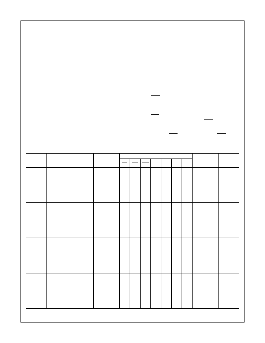
FIGURE 4. SOFTWARE COMMAND CODES AND REGISTER CODES
4-202
82C37A
Software Commands
There are special software commands which can be
executed by reading or writing to the 82C37A. These com-
mands do not depend on the specific data pattern on the
data bus, but are activated by the I/O operation itself. On
read type commands, the data value is not guaranteed.
These commands are:
Clear First/Last Flip-Flop - This command is executed
prior to writing or reading new address or word count infor-
mation to the 82C37A. This command initializes the flip-flop
to a known state (low byte first) so that subsequent accesses
to register contents by the microprocessor will address
upper and lower bytes in the correct sequence.
Set First/Last Flip-Flop - This command will set the flip-flop
to select the high byte first on read and write operations to
address and word count registers.
Master Clear - This software instruction has the same effect
as the hardware Reset. The Command, Status, Request,
and Temporary registers, and Internal First/Last Flip-Flop
and mode register counter are cleared and the Mask register
is set. The 82C37A will enter the idle cycle.
Clear Mask Register - This command clears the mask bits
of all four channels, enabling them to accept DMA requests.
Clear Mode Register Counter - Since only one address
location is available for reading the Mode registers, an inter-
nal two-bit counter has been included to select Mode regis-
ters during read operation. To read the Mode registers, first
execute the Clear Mode Register Counter command, then
do consecutive reads until the desired channel is read. Read
order is channel 0 first, channel 3 last. The lower two bits on
all Mode registers will read as ones.
External EOP Operation
The EOP pin is a bidirectional, open drain pin which may be
driven by external signals to terminate DMA operation.
Because EOP is an open drain pin an external pull-up resis-
tor to V
CC
is required. The value of the external pull-up
resistor used should guarantee a rise time of less than
125ns. It is important to note that the 82C37A will not accept
external EOP signals when it is in a SI (Idle) state. The
controller must be active to latch EXT EOP. Once latched,
the EXT EOP will be acted upon during the next S2 state,
unless the 82C37A enters an idle state first. In the latter
case, the latched EOP is cleared. External EOP pulses
occurring between active DMA transfers in demand mode
will not be recognized, since the 82C37A is in an SI state.
CHANNEL
REGISTER
OPERATION
SIGNALS
FIRST/LAST
FLIP-FLOP
STATE
DATA
BUS
DB0-DB7
CS
IOR
IOW
A3
A2
A1
A0
0
Base and Current Address
Write
0
1
0
0
0
0
0
0
A0-A7
0
1
0
0
0
0
0
1
A8-A15
Current Address
Read
0
0
1
0
0
0
0
0
A0-A7
0
0
1
0
0
0
0
1
A8-A15
Base and Current Word
Count
Write
0
1
0
0
0
0
1
0
W0-W7
0
1
0
0
0
0
1
1
W8-W15
Current Word Count
Read
0
0
1
0
0
0
1
0
W0-W7
0
0
1
0
0
0
1
1
W8-W15
1
Base and Current Address
Write
0
1
0
0
0
1
0
0
A0-A7
0
1
0
0
0
1
0
1
A8-A15
Current Address
Read
0
0
1
0
0
1
0
0
A0-A7
0
0
1
0
0
1
0
1
A8-A15
Base and Current Word
Count
Write
0
1
0
0
0
1
1
0
W0-W7
0
1
0
0
0
1
1
1
W8-W15
Current Word Count
Read
0
0
1
0
0
1
1
0
W0-W7
0
0
1
0
0
1
1
1
W8-W15
2
Base and Current Address
Write
0
1
0
0
1
0
0
0
A0-A7
0
1
0
0
1
0
0
1
A8-A15
Current Address
Read
0
0
1
0
1
0
0
0
A0-A7
0
0
1
0
1
0
0
1
A8-A15
Base and Current Word
Count
Write
0
1
0
0
1
0
1
0
W0-W7
0
1
0
0
1
0
1
1
W8-W15
Current Word Count
Read
0
0
1
0
1
0
1
0
W0-W7
0
0
1
0
1
0
1
1
W8-W15
3
Base and Current Address
Write
0
1
0
0
1
1
0
0
A0-A7
0
1
0
0
1
1
0
1
A8-A15
Current Address
Read
0
0
1
0
1
1
0
0
A0-A7
0
0
1
0
1
1
0
1
A8-A15
Base and Current Word
Count
Write
0
1
0
0
1
1
1
0
W0-W7
0
1
0
0
1
1
1
1
W8-W15
Current Word Count
Read
0
0
1
0
1
1
1
0
W0-W7
0
0
1
0
1
1
1
1
W8-W15
FIGURE 5. WORD COUNT AND ADDRESS REGISTER COMMAND CODES
4-203
82C37A
Application Information
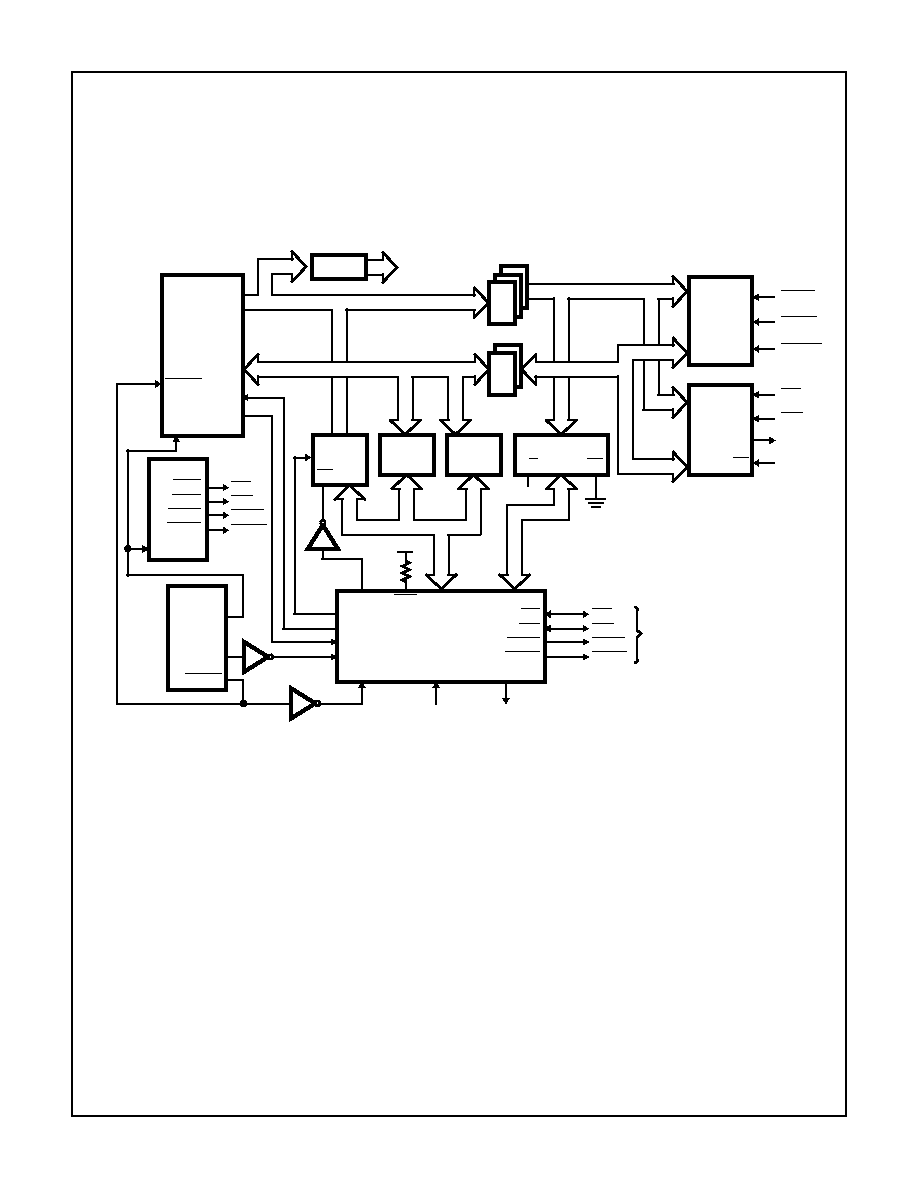
Figure 6 shows an application for a DMA system utilizing the
82C37A DMA controller and the 80C88 Microprocessor. In
this application, the 82C37A DMA controller is used to
improve system performance by allowing an I/O device to
transfer data directly to or from system memory.
Components
The system clock is generated by the 82C84A clock driver
and is inverted to meet the clock high and low times required
by the 82C37A DMA controller. The four OR gates are used
to support the 80C88 Microprocessor in minimum mode by
producing the control signals used by the processor to
access memory or I/O. A decoder is used to generate chip
select for the DMA controller and memory. The most signifi-
cant bits of the address are output on the address/data bus.
Therefore, the 82C82 octal latch is used to demultiplex the
address. Hold Acknowledge (HLDA) and Address Enable
(AEN) are "ORed" together to insure that the DMA controller
does not have bus contention with the microprocessor.
Operation
A DMA request (DREQ) is generated by the I/O device. After
receiving the DMA request, the DMA controller will issue a
Hold request (HRQ) to the processor. The system busses
are not released to the DMA controller until a Hold Acknowl-
edge signal is returned to the DMA controller from the
80C88 processor. After the Hold Acknowledge has been
received, addresses and control signals are generated by
the DMA controller to accomplish the DMA transfers. Data is
transferred directly from the I/O device to memory (or vice
versa) with IOR and MEMW (or MEMR and IOW) being
active. Note that data is not read into or driven out of the
DMA controller in I/O-to-memory or memory-to-I/O data
transfers.
FIGURE 6. APPLICATION FOR DMA SYSTEM
MEMR
MEMW
IOR
IOW
MEMCS
MEMR
MEMW
MEMORY
47k
V
CC
ADDRESS BUS
DATA BUS
V
CC
DATA BUS
80C88
WR
RD
M/IO
HRQ
HLDA
AX
ALE
AD0
AD7
MN/MX
CLK
82C84A
OR
82C85
HLDA
MEMCS
STB
82C82
OE
DECODER
ADDRESS BUS
STB
82C82
OE
A0-7
CS
CLK
EOP
HLDA
IOR
DACK
ADSTB
AEN
DB0-7
IOW
MEMR
MEMW
HRQ
DREQ0
82C37A
IOR
IOW
V
CC
CS
DREQ
I/O
DEVICE
NOTE:
The address lines need pull-up resistors.
4-204
82C37A
Figure 7 shows an application for a DMA system using the
82C37A DMA controller and the 80C286 Microprocessor.
In this application, the system clock comes from the 82C284
clock generator PCLK signal which is inverted to provide
proper READY setup and hold times to the DMA controller in
an 80C286 system. The Read and Write signals from the
DMA controller may be wired directly to the Read/Write con-
trol signals from the 82C288 Bus Controller. The octal latch
for A8-A15 from the DMA controller's data bus is on the local
80C286 address bus so that memory chip selects may still
be generated during DMA transfers. The transceiver on A0-
A7 is controlled by AEN and is not necessary, but may be
used to drive a heavily loaded system address bus during
transfers. The data bus transceivers simply isolate the DMA
controller from the local microprocessor bus and allow pro-
gramming on the upper or lower half of the data bus.
FIGURE 7. 80C286 DMA APPLICATION
MEMW
MEMR
MEMCS
MEMORY
A0 - A23
IOW
DACK
I/O
IOR
SYSTEM
BUS
A0 - A7
TRANSCEIVER
OE
T/R
DEVICE
DREQ
CS
D0 - D15
TRANS-
CEIVER
TRANS-
CEIVER
LATCH
STB
OE
AEN
D0-D7
V
CC
A0-A7
IOR
IOW
MEMR
MEMW
DACK 0-3
D0-D7
DREQ 0-3
EOP
AEN
ADSTB
HRQ
HLDA
CLK
READY
82C37A
IOR
IOW
MEMR
MEMW
TO CORRESPONDING
82C288 SIGNALS AND
MEMORY/PERIPHERALS
D8 - D15
TRANSCEIVER
LATCH
D0 - D7
A8 - A15
DECODE
CHIP SELECT
TO MEMORY/
PERIPHERALS
80C286
A0-A23
D0-D15
READY
HLD
HLDA
CLK
IORC
IOWC
MRDC
MWTC
IOR
IOW
MEMR
MEMW
CLK
82C288
82C284
CLK
PCLK
READY
4-205
82C37A
Absolute Maximum Ratings
Thermal Information
Supply Voltage . . . . . . . . . . . . . . . . . . . . . . . . . . . . . . . . . . . . . +8.0V
Input, Output or I/O Voltage . . . . . . . . . . . GND -0.5V to V
CC
+0.5V
ESD Classification . . . . . . . . . . . . . . . . . . . . . . . . . . . . . . . . Class 1
Operating Conditions
Operating Voltage Range . . . . . . . . . . . . . . . . . . . . . +4.5V to +5.5V
Operating Temperature Range
C82C37A . . . . . . . . . . . . . . . . . . . . . . . . . . . . . . . . 0
o
C to +70
o
C
I82C37A . . . . . . . . . . . . . . . . . . . . . . . . . . . . . . . . -40
o
C to +85
o
C
M82C37A . . . . . . . . . . . . . . . . . . . . . . . . . . . . . . -55
o
C to +125
o
C
Thermal Resistance (Typical)
JA
(
o
C/W)
JC
(
o
C/W)
CERDIP Package . . . . . . . . . . . . . . . .
50
10
CLCC Package . . . . . . . . . . . . . . . . . .
65
14
PDIP Package . . . . . . . . . . . . . . . . . . .
50
N/A
PLCC Package . . . . . . . . . . . . . . . . . .
46
N/A
Storage Temperature Range . . . . . . . . . . . . . . . . . .-65
o
C to +150
o
C
Maximum Junction Temperature Ceramic Package . . . . . . . +175
o
C
Maximum Junction Temperature Plastic Package . . . . . . . . . +150
o
C
Maximum Lead Temperature Package
(Soldering 10s) . . . . . . . . . . . . . . . . . . . . . . . . . . . . . . . . . +300
o
C
(PLCC - Lead Tips Only)
Die Characteristics
Gate Count . . . . . . . . . . . . . . . . . . . . . . . . . . . . . . . . . . . 2325 Gates
CAUTION: Stresses above those listed in "Absolute Maximum Ratings" may cause permanent damage to the device. This is a stress only rating and operation
of the device at these or any other conditions above those indicated in the operational sections of this specification is not implied.
DC Electrical Specifications
V
CC
= +5.0
±
10%, T
A
= 0
o
C to +70
o
C (C82C37A)
T
A
= -40
o
C to +85
o
C (I82C37A)
T
A
= -55
o
C to +125
o
C (M82C37A)
SYMBOL
PARAMETER
MIN
MAX
UNITS
TEST CONDITIONS
VIH
Logical One Input Voltage
2
-
v
C82C37A, I82C37A
2.2
-
V
M82C37A
VIL
Logical Zero Input Voltage
-
0.8
V
VIHC
CLK Input Logical One Voltage
V
CC
-0.8
-
V
VILC
CLK Input Logical Zero Voltage
-
0.8
V
VOH
Output HIGH Voltage
3.0
-
V
IOH = -2.5mA
V
CC
-0.4
-
V
IOH = -100
µ
A
VOL
Output LOW Voltage
-
0.4
V
IOL = +2.5mA all output except EOP,
IOL = +3.2mA for EOP pin 36 only.
II
Input Leakage Current
-1
+1
µ
A
VIN = GND or V
CC
, Pins 6, 7, 11-13, 16-19
IO
Output Leakage Current
-10
+10
µ
A
VOUT = GND or V
CC
, Pins 1-4, 21-23, 26-30,
32-40
ICCSB
Standby Power Supply
Current
-
10
µ
A
V
CC
= 5.5V, VIN = V
CC
or GND, Outputs
Open
ICCOP
Operating Power Supply
Current
-
2
mA/MHz
V
CC
= 5.5V, CLK FREQ = Maximum,
VIN = V
CC
or GND, Outputs Open
Capacitance
T
A
= +25
o
C
SYMBOL
PARAMETER
TYP
UNITS
TEST CONDITIONS
CIN
Input Capacitance
25
pF
FREQ = 1MHz, All measurements are
referenced to device GND
COUT
Output Capacitance
40
pF
CI/O
I/O Capacitance
25
pF
4-206
82C37A
AC Electrical Specifications
V
CC
= +5.0V
±
10%, GND = 0V, T
A
= 0
o
C to +70
o
C (C82C37A),
T
A
= -40
o
C to +85
o
C (I82C37A),
T
A
= -55
o
C to +125
o
C (M82C37A)
SYMBOL
PARAMETER
82C37A-5
82C37A
82C37A-12
UNITS
MIN
MAX
MIN
MAX
MIN
MAX
DMA (MASTER) MODE
(1)TAEL
AEN HIGH from CLK LOW (S1) Delay
Time
-
175
-
105
-
50
ns
(2)TAET
AEN LOW from CLK HIGH (SI) Delay
Time
-
130
-
80
-
50
ns
(3)TAFAB
ADR Active to Float Delay from CLK
HIGH
-
90
-
55
-
55
ns
(4)TAFC
READ or WRITE Float Delay from
CLK HIGH
-
120
-
75
-
50
ns
(5)TAFDB
DB Active to Float Delay from CLK
HIGH
-
170
-
135
-
90
ns
(6)TAHR
ADR from READ HIGH Hold Time
TCY-100
-
TCY-75
-
TCY-65
-
ns
(7)TAHS
DB from ADSTB LOW Hold Time
TCL-18
-
TCL-18
-
TCL-18
-
ns
(8)TAHW
ADR from WRITE HIGH Hold Time
TCY-65
-
TCY-65
-
TCY-50
-
ns
(9)TAK
DACK Valid from CLK LOW
Delay Time
-
170
-
105
-
69
ns
EOP HIGH from CLK HIGH
Delay Time
-
170
-
105
-
90
ns
EOP LOW from CLK HIGH
Delay Time
-
100
-
60
-
35
ns
(10)TASM
ADR Stable from CLK HIGH
-
110
-
60
-
50
ns
(11)TASS
DB to ADSTB LOW Setup Time
TCH-20
-
TCH-20
-
TCH-20
-
ns
(12)TCH
CLK HIGH Time (Transitions 10ns)
70
-
55
-
30
-
ns
(13)TCL
CLK LOW Time (Transitions 10ns)
50
-
43
-
30
-
ns
(14)TCY
CLK Cycle Time
200
-
125
-
80
-
ns
(15)TDCL
CLK HIGH to READ or WRITE LOW
Delay
-
190
-
130
-
120
ns
(16)TDCTR
READ HIGH from CLK HIGH (S4)
Delay Time
-
190
-
115
-
80
ns
(17)TDCTW
WRITE HIGH from CLK HIGH (S4)
Delay Time
-
130
-
80
-
70
ns
(18)TDQ
HRQ Valid from CLK HIGH
Delay Time
-
120
-
75
-
30
ns
(19)TEPH
EOP Hold Time from CLK LOW (S2)
90
-
90
-
50
-
ns
(20)TEPS
EOP LOW to CLK LOW Setup Time
40
-
25
-
0
-
ns
4-207
82C37A
(21)TEPW
EOP Pulse Width
220
-
135
-
50
-
ns
(22)TFAAB
ADR Valid Delay from CLK HIGH
-
110
-
60
-
50
ns
(23)TFAC
READ or WRITE Active from
CLK HIGH
-
150
-
90
-
50
ns
(24)TFADB
DB Valid Delay from CLK HIGH
-
110
-
60
-
45
ns
(25)THS
HLDA Valid to CLK HIGH Setup Time
75
-
45
-
10
-
ns
(26)TIDH
Input Data from MEMR HIGH
Hold Time
0
-
0
-
0
-
ns
(27)TIDS
Input Data to MEMR HIGH
Setup Time
155
-
90
-
45
-
ns
(28)TODH
Output Data from MEMW HIGH
Hold Time
15
-
15
-
TCY-50
-
ns
(29)TODV
Output Data Valid to MEMW HIGH
TCY-35
-
TCY-35
-
TCY-10
-
ns
(30)TQS
DREQ to CLK LOW (SI, S4)
Setup Time
0
-
0
-
0
-
ns
(31)TRH
CLK to READY LOW Hold Time
20
-
20
-
10
-
ns
(32)TRS
READY to CLK LOW Setup Time
60
-
35
-
15
-
ns
(33)TCLSH
ADSTB HIGH from CLK LOW
Delay Time
-
80
-
70
-
70
ns
(34)TCLSL
ADSTB LOW from CLK LOW
Delay Time
-
120
-
120
-
60
ns
(35)TWRRD
READ HIGH Delay from WRITE HIGH
0
-
0
-
5
-
ns
(36)TRLRH
READ Pulse Width, Normal Timing
2TCY-60
-
2TCY-60
-
2TCY-55
-
ns
(37)TSHSL
ADSTB Pulse Width
TCY-80
-
TCY-50
-
TCY-35
-
ns
(38)TWLWHA
Extended WRITE Pulse Width
2TCY-100
-
2TCY-85
-
2TCY-80
-
ns
(39)TWLWH
WRITE Pulse Width
TCY-100
-
TCY-85
-
TCY-80
-
ns
(40)TRLRHC
READ Pulse Width, Compressed
TCY-60
-
TCY-60
-
TCY-55
-
ns
(56)TAVRL
ADR Valid to READ LOW
17
-
17
-
17
-
ns
(57)TAVWL
ADR Valid to WRITE LOW
7
-
7
-
7
-
ns
(58)TRHAL
READ HIGH to AEN LOW
15
-
15
-
15
-
ns
(59)TRHSH
READ HIGH to ADSTB HIGH
13
-
13
-
13
-
ns
(60)TWHSH
WRITE HIGH to ADSTB HIGH
15
-
15
-
15
-
ns
(61)TDVRL
DACK Valid to READ LOW
25
-
25
-
25
-
ns
AC Electrical Specifications
V
CC
= +5.0V
±
10%, GND = 0V, T
A
= 0
o
C to +70
o
C (C82C37A),
T
A
= -40
o
C to +85
o
C (I82C37A),
T
A
= -55
o
C to +125
o
C (M82C37A) (Continued)
SYMBOL
PARAMETER
82C37A-5
82C37A
82C37A-12
UNITS
MIN
MAX
MIN
MAX
MIN
MAX
4-208
82C37A
(62)TDVWL
DACK Valid to WRITE LOW
25
-
25
-
25
-
ns
(63)TRHDI
READ HIGH to DACK Inactive
12
-
12
-
12
-
ns
(64)TAZRL
ADR Float to READ LOW
-2.5
-
-2.5
-
-2.5
-
ns
PERIPHERAL (SLAVE) MODE
(41)TAR
ADR Valid or CS LOW to READ LOW
10
-
10
-
0
-
ns
(42)TAWL
ADR Valid to WRITE LOW Setup Time
0
-
0
-
0
-
ns
(43)TCWL
CS LOW to WRITE LOW Setup Time
0
-
0
-
0
-
ns
(44)TDW
Data Valid to WRITE HIGH Setup Time
150
-
100
-
60
-
ns
(45)TRA
ADR or CS Hold from READ HIGH
0
-
0
-
0
-
ns
(46)TRDE
Data Access from READ
-
140
-
120
-
80
ns
(47)TRDF
DB Float Delay from READ HIGH
5
85
5
85
5
55
ns
(48)TRSTD
Power Supply HIGH to RESET LOW
Setup Time
500
-
500
-
500
-
ns
(49)TRSTS
RESET to First IOR or IOW
2TCY
-
2TCY
-
2TCY
-
ns
(50)TRSTW
RESET Pulse Width
300
-
300
-
300
-
ns
(51)TRW
READ Pulse Width
200
-
155
-
85
-
ns
(52)TWA
ADR from WRITE HIGH Hold Time
0
-
0
-
0
-
ns
(53)TWC
CS HIGH from WRITE HIGH
Hold Time
0
-
0
-
0
-
ns
(54)TWD
Data from WRITE HIGH Hold Time
10
-
10
-
10
-
ns
(55)TWWS
WRITE Pulse Width
150
-
100
-
45
-
ns
AC Electrical Specifications
V
CC
= +5.0V
±
10%, GND = 0V, T
A
= 0
o
C to +70
o
C (C82C37A),
T
A
= -40
o
C to +85
o
C (I82C37A),
T
A
= -55
o
C to +125
o
C (M82C37A) (Continued)
SYMBOL
PARAMETER
82C37A-5
82C37A
82C37A-12
UNITS
MIN
MAX
MIN
MAX
MIN
MAX
4-209
82C37A
Timing Waveforms
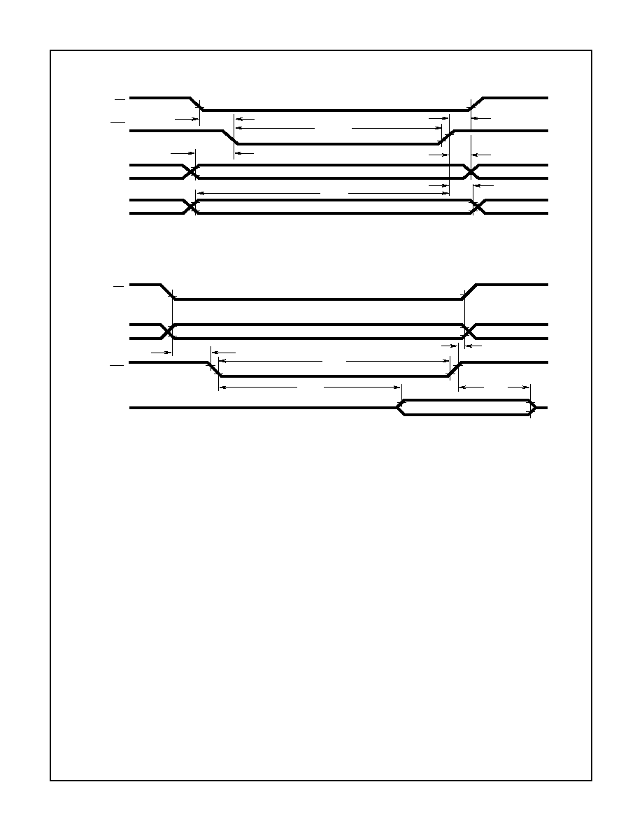
FIGURE 8. SLAVE MODE WRITE
NOTE:
Successive WRITE accesses to the 82C37A must allow at least TCY as recovery time between accesses. A TCY recovery time must
be allowed before executing a WRITE access after a READ access.
FIGURE 9. SLAVE MODE READ
NOTE:
Successive READ accesses to the 82C37A must allow at least TCY as recovery time between accesses. A TCY recovery time must
be allowed before executing a READ access after a WRITE access.
CS
A0 - A3
IOW
DB0 - DB7
INPUT VALID
INPUT VALID
TWWS
(55)
TDW
(44)
TCWL
(43)
TAWL
(42)
TWC (53)
TWA (52)
TWD (54)
CS
A0 - A3
IOR
DB0 -DB7
ADDRESS MUST BE VALID
TAR
(41)
TRDE
(46)
TRDF
(47)
TRA (45)
TRW
(51)
DATA OUT VALID
4-210
82C37A
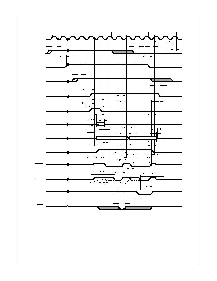
FIGURE 10. DMA TRANSFER
Timing Waveforms
(Continued)
TEPW (21)
TAK (9)
SI
SI
TQS
(30)
S0
S0
S1
S2
S3
S4
S2
S3
S4
SI
SI
SI
TDQ
(18)
THS
(25)
TAEL
(1)
TCLSH
(33)
TQS
(30)
TCL (13)
TCY
(14)
TCH
(12)
TDQ
(18)
TAET
(2)
TSHSL
(37)
TCLSL
(34)
TEPS
(20)
TEPH
(19)
TRHAL
(58)
TAK (9)
TAFAB (3)
TAHW (8)
TAHR (6)
TRHDI (63)
TAFC (4)
TDCTR (16)
TDCL
(15)
CLK
DREQ
HRQ
HLDA
AEN
ADSTB
DB0-DB7
A0-A7
DACK
READ
WRITE
INT EOP
EXT EOP
(64)
TAZRL
TAFDB
(5)
TFAAB
(22)
TFADB
(24)
TASS
(11)
TAHS
(7)
A8-A15
TAK
(9)
TDCL
(15)
TFAC
(23)
TDCL (15)
TDVWL
(62)
TWLWHA
(38)
TDCTW
(17)
TAVWL
(57)
TDVAL (61)
(FOR EXTENDED WRITE)
(FOR EXTENDED WRITE)
TAK (9)
TDCL
(15)
TWLWH (39)
TDCTW (17)
TWRRD
(35)
TAVRL
(56)
TRLRH
(36)
TDCTR
(16)
TAHR
(6)
TAHW
(8)
TASM
(10)
ADDRESS VALID
ADDRESS VALID
4-211
82C37A
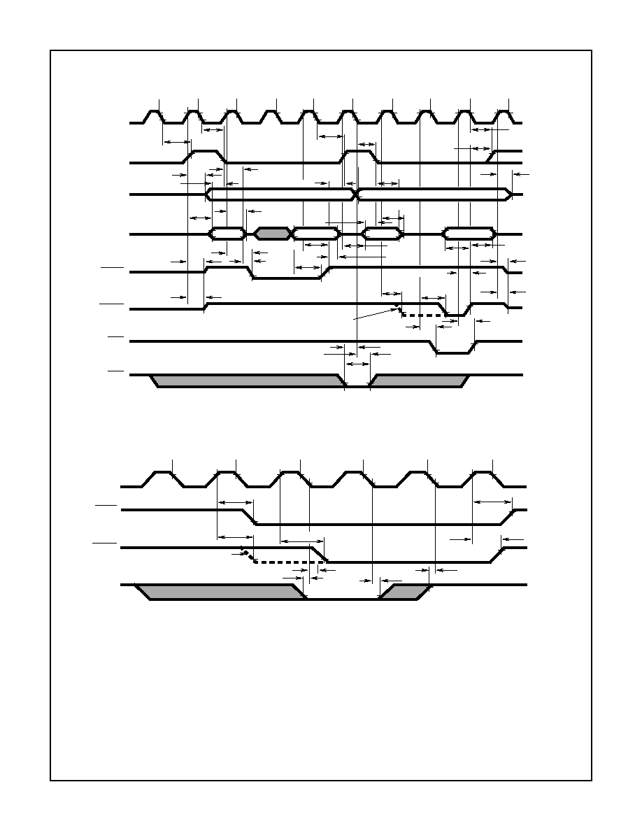
FIGURE 11. MEMORY-TO-MEMORY TRANSFER
FIGURE 12. READY
NOTE: READY must not transition during the specified setup and hold times.
Timing Waveforms
(Continued)
S0
(33)
TCLSH
CLK
S11
S12
S13
S14
S21
S22
S23
S24
S11/SI
ADSTB
A0-A7
DB0-DB7
MEMR
MEMW
EOP
EXT EOP
(34)
TCLSL
(7)
TAHS
TFAAB (22)
TASS (11)
TFADB (24)
(5) TAFDB
IN
A8-A15
(16) TDCTR
TFAC (23)
TFAC (23)
ADDRESS VALID
ADDRESS VALID
(33)
TCLSH
(34)
TCLSL
TWHSH
(60)
TCLSH
(33)
TAFAB
(3)
TAFC
(4)
TAFC
(4)
(59) TRHSH
TAHS
(7)
A8-A15
(24)
TFADB
TIDH (26)
TIDS
(27)
TAFDB
(5)
TDCL
(15)
TDCL
(15)
TDCTW (17)
TAK
(9)
TAK
(9)
OUT
TEPW
(21)
TEPS (20)
(19) TEPH
EXTENDED WRITE
TOVD
(29)
TODH (28)
TAZRL
(64)
TDCL
(15)
TASS
(11)
CLK
EXTENDED WRITE
(16)
TDCTR
S4
SW
SW
S3
S2
(15)
TDCL
(15)
TDCL
(15)TDCL
(31)TRH
(32)TRS
TRH
(32)TRS
(17)
TDCTW
READ
WRITE
READY
(31)
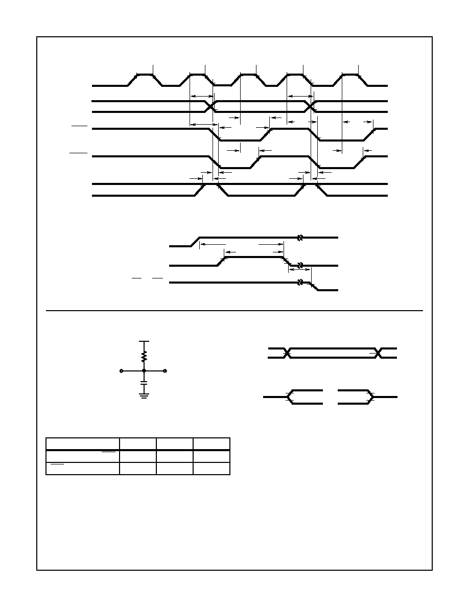
4-212
82C37A
AC Test Circuits
AC Testing Input, Output Waveforms
FIGURE 13. COMPRESSED TRANSFER
FIGURE 14. RESET
Timing Waveforms
(Continued)
CLK
S4
S2
(10)
TASM
(15)
TDCL
TRLRHC
(40)
TDCTR
(16)
TDCL
(15)
(10)
TASM
TDCTR
(16)
TDCTW
(17)
TRH (31)
TRS (32)
S2
S4
TRS (32)
TRH (31)
TDCTW
(17)
A0-A7
READ
WRITE
READY
VALID
VALID
(48) TRSTD
(50) TRSTW
(49) TRSTS
IOR OR IOW
RESET
V
CC
TEST CONDITION DEFINITION TABLE
PINS
V1
R1
C1
All Outputs Except EOP
1.7V
520
100pF
EOP
V
CC
1.6k
50pF
TEST POINT
R1
V1
C1 (NOTE)
OUTPUT FROM
DEVICE UNDER
TEST
NOTE:
Includes STRAY and FIXTURE Capacitance
NOTE:
AC Testing: All AC Parameters tested as per test circuits.
Input RISE and FALL times are driven at Ins/V. CLK input
must switch between VIHC +0.4V and VILC -0.4V
VOH
VO -0.45
0.45
VOL
OUTPUT
L OR H
Z
VOH
2.0V
0.8V
VOL
INPUT
Z
L OR H
VIH + 0.4V
VIL - 0.4V
1.5V
1.5V
VOH
VOL
OUTPUT
OUTPUT
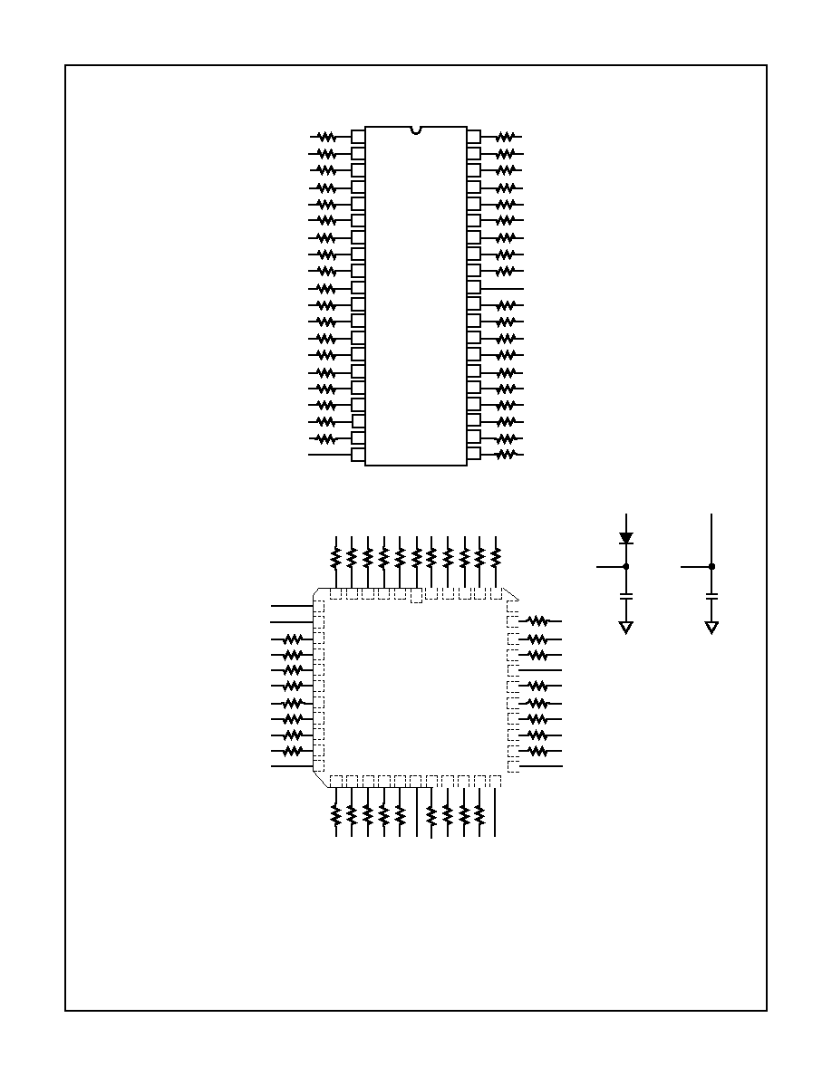
4-213
82C37A
Burn-In Circuits
MD82C37A CERDIP
MR82C37A CLCC
NOTES:
1. V
CC
= 5.5V
±
0.5V
2. VIH = 4.5V
±
10%
3. VIL = -0.2V to 0.4V
4. GND = 0V
5. R1 = 1.2k
±
5%
6. R2 = 47k
±
5%
7. C1 = 0.01
µ
F minimum
8. C2 = 0.1
µ
F minimum
9. D1 = 1N4002
10. F0 = 100kHz
±
10%
11. F1 = F0/2, F2 = F1/2,..., F15 = F14/2
12. DO0 - DO6 are outputs from the 82C82 Octal Latching Bus Driver
DO5
VCC/2
VCC/2
VCC/2
A
DO5
VCC/2
VCC/2
VCC/2
DO5
F1
DO6
VCC/2
F12
F13
F14
F15
GND
VCC
33
34
35
36
37
38
40
32
31
30
29
24
25
26
27
28
21
22
23
13
2
3
4
5
6
7
8
9
10
11
12
14
15
16
17
18
19
20
39
1
VCC/2
VCC/2
VCC/2
A
VCC
DO1
VCC
DO0
B
DO2
DO3
DO4
F10
VCC/2
VCC/2
F8
DO4
F7
VCC/2
VCC/2
F9
R1
R1
R1
R1
R1
R1
R2
R1
R2
R2
R2
R2
R2
R2
R1
R1
R2
R2
R2
R1
R2
R1
R1
R1
R1
R3
R1
R1
R1
R2
R2
R2
R2
R1
R1
R1
R1
R1
VCC/2
VCC/2
F8
F14
F13
F12
VCC/2
F15
GND
DO4
OPEN
DO5
VCC/2
VCC/2
DO5
F1
D06
VCC/2
OPEN
VCC/2
14
13
12
11
10
9
8
7
17
16
15
2
5
30
35
39
38
37
36
33
34
32
31
29
4
6
3
1
40
41
42
43
44
A
VCC/2
VCC/2
VCC/2
VCC/2
VCC/2
VCC/2
A
V
CC
DO1
B
DO2
DO3
DO4
F10
F9
V
CC
VCC/2
V
CC
DO5
OPEN
OPEN
DO4
28
27
26
25
24
23
22
21
20
19
18
V
CC
V
CC
D1
C1
C1
A
B
4-214
Die Characteristics
DIE DIMENSIONS:
148 x 159 x 19
±
1mils
(3760- x 4040 x 525
µ
m)
METALLIZATION:
Type: SiAlCu
Thickness: Metal 1: 8k
≈
±
0.75k
≈
Thickness: Metal 2: 12k
≈
±
1.0k
≈
GLASSIVATION:
Type: Nitrox
Thickness: 10k
≈
±
3k
≈
WORST CASE CURRENT DENSITY:
0.6 x 10
5
A/cm
2
Metallization Mask Layout
82C37A
82C37A