 | –≠–ª–µ–∫—Ç—Ä–æ–Ω–Ω—ã–π –∫–æ–º–ø–æ–Ω–µ–Ω—Ç: CA1394 | –°–∫–∞—á–∞—Ç—å:  PDF PDF  ZIP ZIP |
8-9
May 1999
CA1391, CA1394
TV Horizontal Processors
CAUTION: These devices are sensitive to electrostatic discharge. Users should follow proper IC Handling Procedures.
Copyright
©
Harris Corporation 1999
File Number
981.4
Features
∑ CA1391E - Positive Horizontal Sawtooth Input
∑ CA1394E - Negative Horizontal Sawtooth Input
∑ Internal Shunt Regulator
∑ Linear Balanced Phase Detector
∑ Preset Hold Control Capability
∑ Pull-In
. . . . . . . . . . . . . . . . . . . . . . . . . . . . . . . . ±
300Hz (Typ)
∑ Low Thermal Frequency Drift
∑ Small Static Phase Error
∑ Variable Output Duty Cycle
∑ Adjustable DC Loop Gain
Description
The Harris CA1391E and CA1394E are monolithic
integrated circuits designed for use in the low-level
horizontal section of monochrome or color television
receivers. Functions include a phase detector, an oscillator,
a regulator, and a pre-driver.
The CA1391E and CA1394E are electrically equivalent and
pin compatible with industry types 1391 and 1394 in similar
packages.
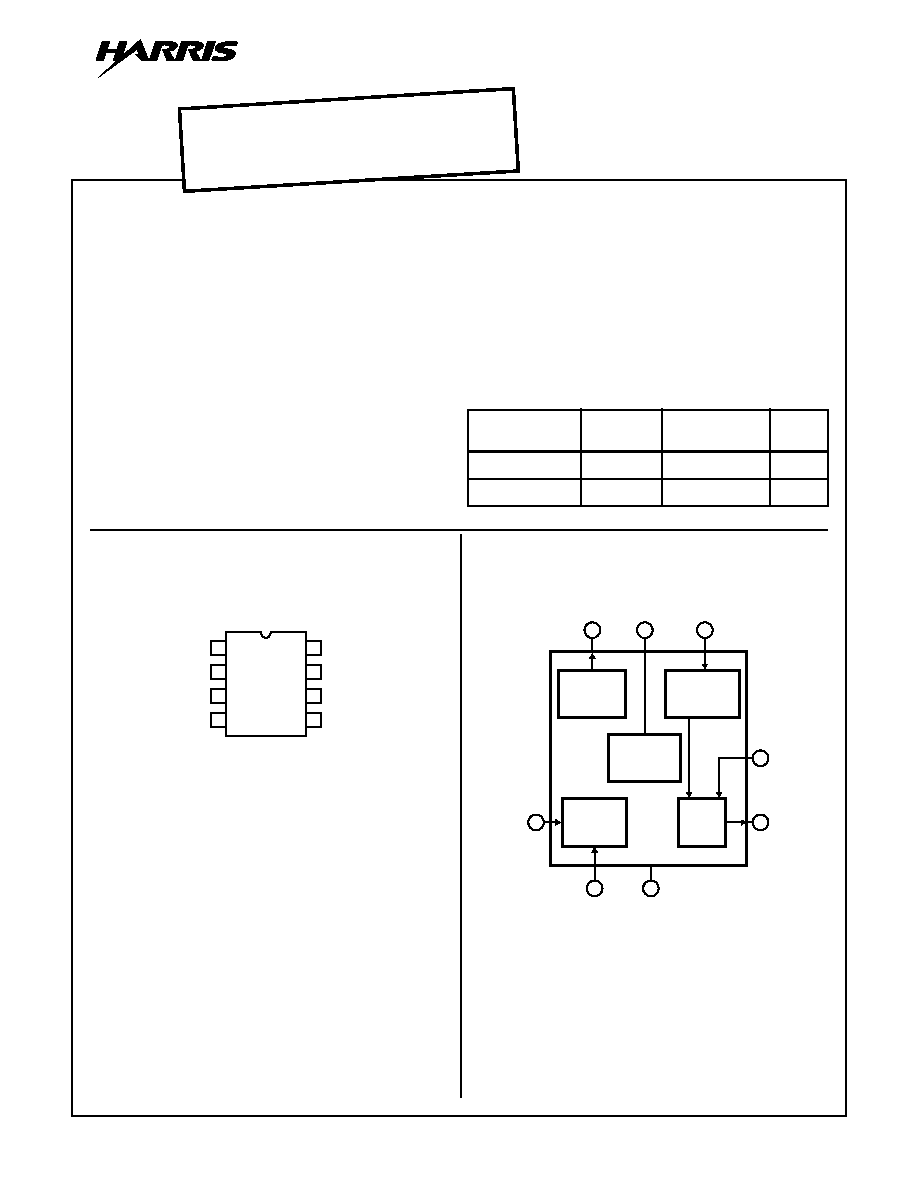
Pinout
CA1391, CA1394
(PDIP)
TOP VIEW
Functional Diagram
Part Number Information
PART NUMBER
TEMP.
RANGE (
o
C)
PACKAGE
PKG.
NO.
CA1391E
0 to 85
8 Ld PDIP
E8.3
CA1394E
0 to 85
8 Ld PDIP
E8.3
OUT
GND
SYNC
HORIZ
1
2
3
4
8
7
6
5
SPACE
OSC
V+
PHASE
RATIO
TIMING
DETECT
OUT
IN
IN
MARK-
PHASE
DETECTOR
OUT
PHASE
DETECTOR
REGULATOR
OSCILLATOR
PRE-
DRIVER
HORIZONTAL
SAWTOOTH
INPUT
SYNC
INPUT
GROUND
MARK-SPACE
RATIO
OUTPUT
V+
PHASE
DETECTOR
OUTPUT
OSCILLATOR
TIMING
4
3
2
6
7
5
8
1
[ /Title
(CA13
91,
CA139
4)
/Sub-
ject
(TV
Hori-
zontal
Proces-
sors)
/Autho
r ()
/Key-
words
(Har-
ris
Semi-
con-
ductor,
TV
hori-
zontal
proces-
sor,
hori-
zontal
oscilla-
tor,
hori-
zontal
driver,
phase
detec-
tor,
AFC
cir-
cuit,
AGC
cir-
cuit,
OBSOLETE PRODUCT
NO RECOMMENDED REPLA
CEMENT
Call Central Applications 1-800-442-7747
or email: centapp@harris.com
8-10
Absolute Maximum Ratings
Thermal Information
DC Supply Current . . . . . . . . . . . . . . . . . . . . . . . . . . . . . . . . . 40mA
DC Output Voltage . . . . . . . . . . . . . . . . . . . . . . . . . . . . . . . . . . . 40V
DC Output Current . . . . . . . . . . . . . . . . . . . . . . . . . . . . . . . . . 30mA
Sync Input Voltage . . . . . . . . . . . . . . . . . . . . . . . . . . . . . . . . . 5V
P-P
Sawtooth Input Voltage. . . . . . . . . . . . . . . . . . . . . . . . . . . . . . 5V
P-P
Operating Conditions
Temperature Range . . . . . . . . . . . . . . . . . . . . . . . . . . . 0
o
C to 85
o
C
Thermal Resistance (Typical, Note 1)
JA
(
o
C/W)
PDIP Package . . . . . . . . . . . . . . . . . . . . . . . . . . . . .
120
Maximum Junction Temperature (Plastic Package) . . . . . . . . 150
o
C
Maximum Storage Temperature Range . . . . . . . . . -65
o
C to 150
o
C
Maximum Lead Temperature (Soldering 10s) . . . . . . . . . . . . . 300
o
C
CAUTION: Stresses above those listed in "Absolute Maximum Ratings" may cause permanent damage to the device. This is a stress only rating and operation
of the device at these or any other conditions above those indicated in the operational sections of this specification is not implied.
NOTE:
1.
JA
is measured with the component mounted on an evaluation PC board in free air.
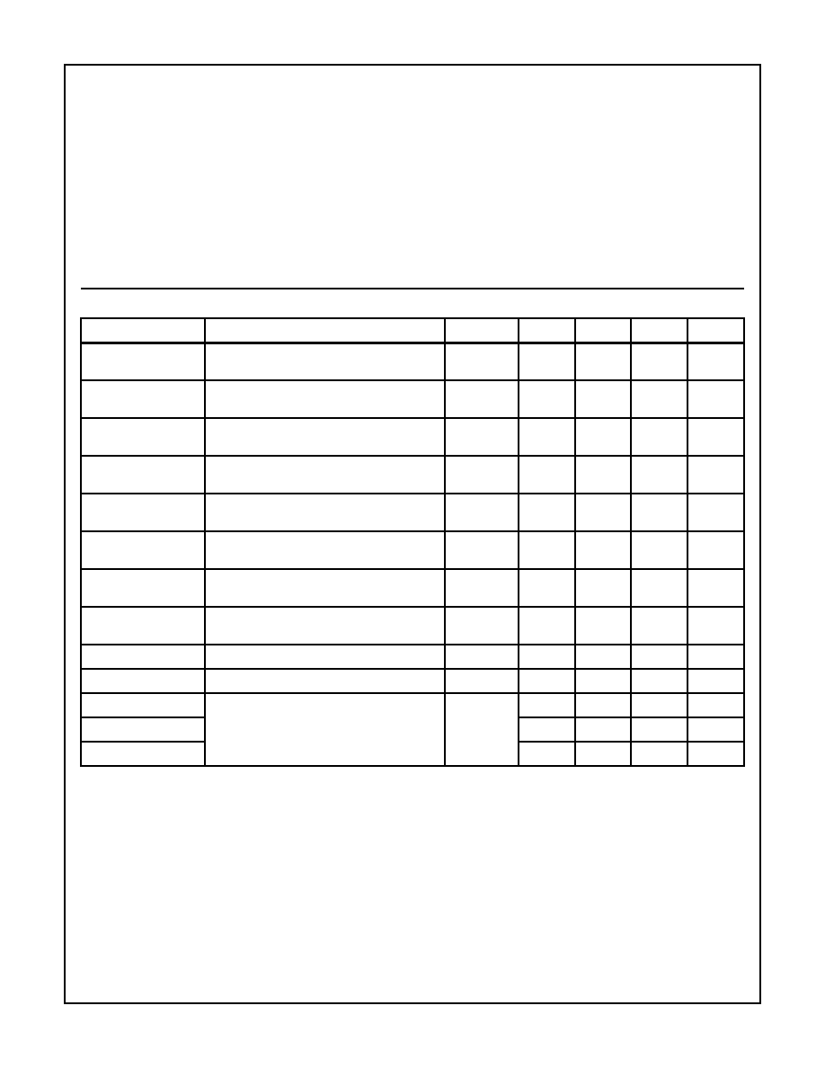
Electrical Specifications
(See Figure 1)
PARAMETER
TEST CONDITIONS
TEMP. (
o
C)
MIN
TYP
MAX
UNITS
Supply Voltage
S
1
, S
5
, S
6
= 2; S
2
, S
3
, S
4
, S
7
, S
8
= 1
Measure Terminal 6 to GND
25
8
-
9
V
Free Running
Frequency -1%
S
1
, S
5
, S
6
= 2; S
2
, S
3
, S
4
, S
7
, S
8
= 1
Counter to Terminal 1
25
14734
-
16734
Hz
Output Leakage
S
2
, S
3
, S
6
, S
8
= 1; S
1
, S
4
, S
5
, S
7
= 2
Measure Terminal 1 to 25V
25
-
10
-
mV
Output Saturation
S
2
, S
3
, S
5
, S
6
, S
8
= 1; S
1
, S
4
, S
7
= 2
Measure Terminal 1 to GND
25
-
60
-
mV
Phase Detector Bias
S
2
, S
5
, S
6
, S
8
= 1; S
1
, S
3
, S
4
, S
7
= 2
Measure Terminal 3 to GND
25
-
1.9
-
V
Phase Detector Leak
S
5
, S
8
= 1; S
1
, S
2
, S
3
, S
4
, S
6
, S
7
= 2
Measure Terminal 5 to +4V
25
-2
-
2
mV
Phase Detector Low
S
1
, S
5
, S
8
= 1; S
2
, S
3
, S
4
, S
6
, S
7
= 2
Measure Terminal 5 to +4V
25
-0.55
(Note 2)
-
-
V
Phase Detector High
S
1
, S
5
, S
6
, S
8
= 1; S
2
, S
3
, S
4
, S
7
= 2
Measure Terminal 5 to +4V
25
+0.55
(Note 2)
-
-
V
Phase Detector Balance V
DET2
+ V
DET3
25
-100
-
100
mV
Sync Diode
S
1
, S
2
, S
3
, S
4
, S
6
, S
7
= 1; S
5
, S
8
= 2
25
0.3
-
1.2
V
Static Phase Error
See Figure 3
25
-
0.5
-
µ
s
Oscillator Pull In Range
-
±
300
-
Hz
Oscillator Hold In Range
-
±
900
-
Hz
NOTE:
2. Polarity reversed in the CA1391.
CA1391, CA1394
8-11
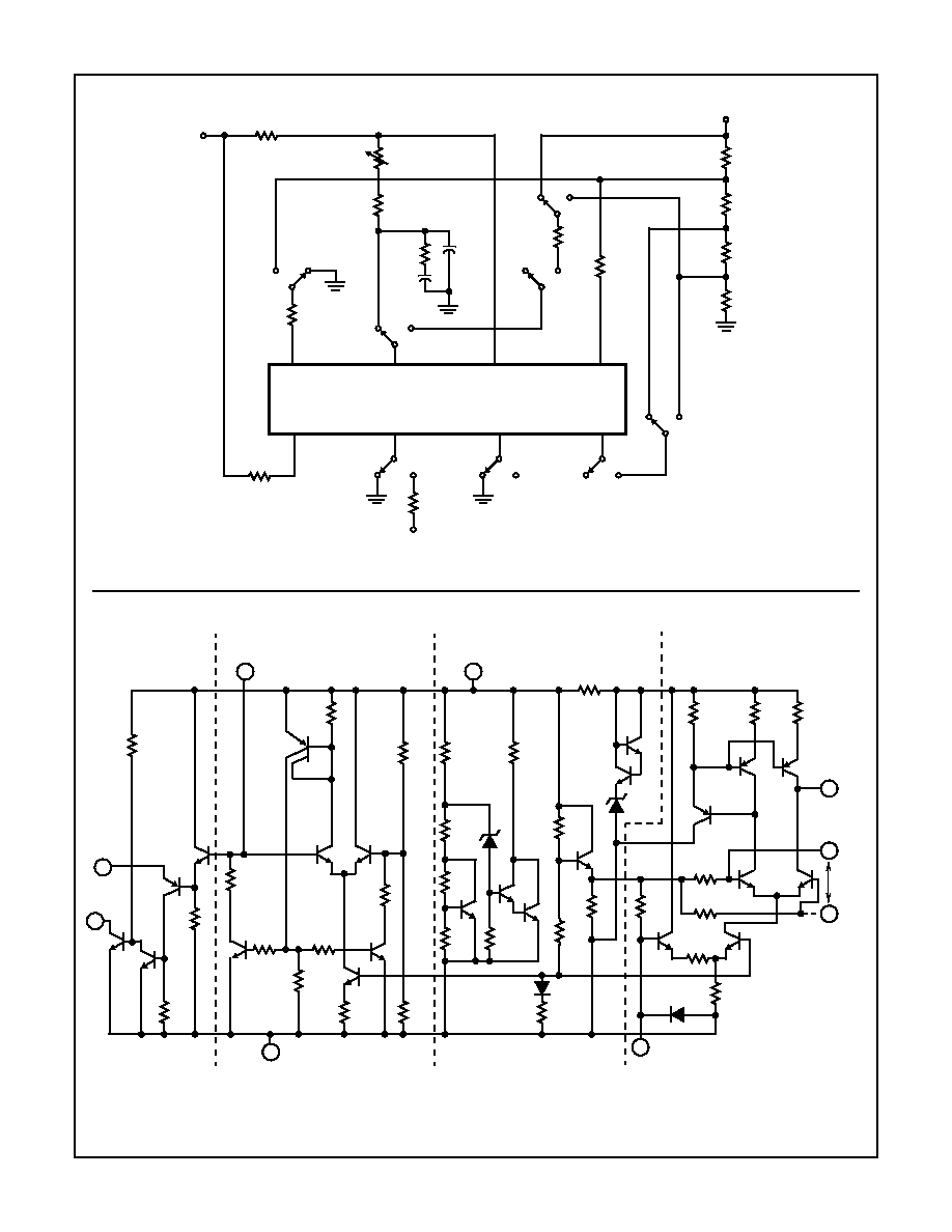
Test Circuit
Schematic Diagram
2
S
5
+25V
620
1W
2.65k
1
1.5k
150k
14k
1k
1
2
S
4
1
µ
F
6800pF
1
2
1
2
1
2
1
2
S
2
S
1
S
8
S
7
1
2
430
1.65k
200
150
100
150
8
7
6
5
4
3
2
1
5.6k
+6V
CA1391/CA1394
S
6
+6V
S
3
2
1
FIGURE 1. DC TEST CIRCUIT
REGULATOR
Q
6
OSCILLATOR
PHASE
DETECTOR
V+
OUT
SYNC INPUT
GND
MARK-
SPACE
RATIO
PRE-
DRIVER
OSC.
TIMING
Q
4
Q
3
Q
1
Q
2
Q
5
Q7 Q
8
R
1
2.6K
R
4
430
R
3
7.5K
R
2
6.8K
R
6
400
R
5
5.1K
R
12
2.4K
R
9
1.3K
Q
10
Q
9
R
10
470
R
11
3.6K
R
16
1.1K
R
18
200
R
14
6.8K
R
15
2.4K
R
13
1.5K
Q
12
Q
13
D
1
R
19
240
R
20
820
R
22
3.3K
Q
14
Z
2
R
1
3K
Q
15
R
31
560
Q
16
Z
1
Q
19
R
23
6.8K
Q
20
Q
21
Q
22
Q
23
CA1391E
R
28
910
Q
17
Q
18
D
2
R
27
510
R
26
7.5K
R
25
7.5K
HORIZ
INPUT
CA1394E
PHASE
DET. OUT
6
7
8
1
2
3
4
4
5
R
7
1.8K
R
8
3.9K
R
24
40K
R
29
1.5K
R
30
1.5K
R
17
6.2K
Q
11
NOTE: All resistances are in ohms.
CA1391, CA1394

8-12
Application Information
Circuit Operation
(See Schematic Diagram)
The CA1391 and CA1394 contain the oscillator, phase
detector, and predriver sections necessary for the television
horizontal oscillator and AFC loop.
The oscillator is an RC type with Terminal 7 used to control the
timing. If it is assumed that Q
7
is initially off, then an external
capacitor connected from Terminal 7 to ground charges through
an external resistance connected between Terminals 6 and 7. As
soon as the voltage at Terminal 7 exceeds the potential set at the
base of Q
8
by resistors R
11
and R
12
, Q
7
turns on, and Q
6
sup-
plies base current to Q
5
and Q
10
. Transistor Q
5
discharges the
capacitor through R
4
until the base bias of Q
7
falls below that of
Q
8
at which time, Q
7
turns off, and the cycle repeats.
The sawtooth generated at the base of Q
4
appears across R
3
and turns off Q
3
whenever the sawtooth voltage rises to a value
that exceeds the bias set at Terminal 8. By adjusting the poten-
tial at Terminal 8, the duty cycle at the pre-drive output (Termi-
nal 1) may be changed. The phase detector is isolated from the
remainder of the circuit by R
31
, Z
2
, Q
15
and Q
16
. The phase
detector consists of the comparator Q
22
and Q
23
, and the
gated current source Q
18
. Negative going sync pulses at Ter-
minal 3 turn off Q
17
, and the current division between Q
22
and
Q
23
is then determined by the phase relationship of the sync
and the sawtooth waveform at Terminal 4, which is derived from
the horizontal flyback pulse. If there is no phase difference
between the sync and sawtooth, equal currents flow in the col-
lectors of Q
22
and Q
23
during each half of the sync pulse
period. The current in Q
22
is turned around by current mirror
Q
20
and Q
21
so that there is no net output current at Terminal 5
for balanced conditions. When a phase offset occurs, current
flows either in or out of Terminal 5. In circuit applications, this
terminal is connected to Terminal 7 through an external low
pass filter, thereby controlling the oscillator.
Shunt regulation for the circuit is obtained by using a V
BE
and zener multiplier. Resistors R
13
and R
14
multiply the V
BE
of Q
11
, and the ratio of R
15
and R
16
multiplies the voltage of
the zener diode Z
1
.
POSITIVE PULSE WIDTH AT TERMINAL 1 (
µ
s)
70
60
50
40
30
20
10
0
2.0
2.5
3.0
3.5
4.0
4.5
5.0
V
O
L
T
A
GE A
T
TERM. 8 (THR
OUGH 1k
)
T
A
= 25
o
C
FREE RUNNING FREQUENCY = 15734Hz
FIGURE 2. DUTY CYCLE AT THE PRE-DRIVE OUTPUT (TERMINAL
1) AS IT IS AFFECTED BY THE INPUT AT TERMINAL 8
8
7
6
5
4
3
2
1
CA1394
2
470
µ
F
0.47
µ
F
0.01
µ
F
3k
620
24V
V+
470pF
120k
6800pF
14k
2.7k
2.4k
1.5k
4k
10W
0.001
µ
F
+150V
270
1.2k
0.0027
µ
F
150k
8.2k
0.1
µ
F
0.1
µ
F
390k
3.9k
22
7.5k
SYNC
20V
P-P
5
µ
s
60V
P-P
10
µ
s
FIGURE 3. TYPICAL CIRCUIT APPLICATION
CA1391, CA1394