1
Semiconductor
CAUTION: These devices are sensitive to electrostatic discharge; follow proper IC Handling Procedures.
Copyright
©
Harris Corporation 1998
HA-2840
600MHz, Very High Slew Rate
Operational Amplifier
The HA-2840 is a wideband, very high slew rate, operational
amplifier featuring superior speed and bandwidth
characteristics. Bipolar construction, coupled with dielectric
isolation, delivers outstanding performance in circuits with a
closed loop gain of 10 or greater.
A 625V/
µ
s slew rate and a 600MHz gain bandwidth product
ensure high performance in video and RF amplifier designs.
Differential gain and phase are a low 0.03% and 0.03
degrees respectively, making the HA-2840 ideal for video
applications. A full
±
10V output swing, high open loop gain,
and outstanding AC parameters, make the HA-2840 an
excellent choice for high speed Data Acquisition Systems.
The HA-2840 is available in commercial and industrial
temperature ranges, and a choice of packages. See the
"Ordering Information" below for more information. For
military grade product, refer to the HA-2840/883 data sheet.
Features
∑ Low Supply Current . . . . . . . . . . . . . . . . . . . . . . . . . 13mA
∑ Very High Slew Rate . . . . . . . . . . . . . . . . . . . . . . 625V/
µ
s
∑ Open Loop Gain . . . . . . . . . . . . . . . . . . . . . . . . . . . 25kV/V
∑ Wide Gain-Bandwidth (A
V
10) . . . . . . . . . . . . . . 600MHz
∑ Full Power Bandwidth . . . . . . . . . . . . . . . . . . . . . . . 10MHz
∑ Low Offset Voltage . . . . . . . . . . . . . . . . . . . . . . . . . .0.6mV
∑ Differential Gain/Phase. . . . . . . . . . . 0.03%/0.03 Degrees
∑ Enhanced Replacement for EL2039
Applications
∑ Pulse and Video Amplifiers
∑ Wideband Amplifiers
∑ High Speed Sample-Hold Circuits
∑ RF Oscillators
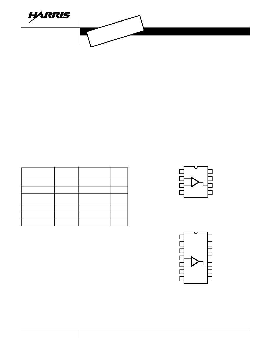
Pinouts
HA-2840
(CERDIP, PDIP, SOIC)
TOP VIEW
HA-2840
(PDIP)
TOP VIEW
NOTE: No Connection (NC) pins may be tied to a ground plane for
better isolation and heat dissipation.
Part Number Information
PART NUMBER
(BRAND)
TEMP.
RANGE (
o
C)
PACKAGE
PKG.
NO.
HA3B2840-5
0 to 75
14 Ld PDIP
E14.3
HA3-2840-5
0 to 75
8 Ld PDIP
E8.3
HA9P2840-5
(H28405)
0 to 75
8 Ld SOIC
M8.15
HA3B2840-9
-40 to 85
14 Ld PDIP
E14.3
HA7-2840-9
-40 to 85
8 Ld CERDIP
F8.3A
HA3-2840-9
-40 to 85
8 Ld PDIP
E8.3
NC
-IN
+IN
V-
1
2
3
4
8
7
6
5
NC
V+
OUT
NC
+
-
NC
NC
NC
-IN
+IN
V-
NC
NC
NC
NC
V+
OUT
NC
NC
1
2
3
4
5
6
7
14
13
12
11
10
9
8
+
-
September 1998
File Number
2842.3
OBSOLETE PR
ODUCT
See HA-2540 or HA-2850
2
Absolute Maximum Ratings
Thermal Information
Voltage Between V+ and V- Terminals. . . . . . . . . . . . . . . . . . . . 35V
Differential Input Voltage . . . . . . . . . . . . . . . . . . . . . . . . . . . . . . . 6V
Output Current . . . . . . . . . . . . . . . . . . . . . . . . . . . . . . . . . . . . . 50mA
Operating Conditions
Temperature Range
HA-2840-5 . . . . . . . . . . . . . . . . . . . . . . . . . . . . . . . . 0
o
C to 75
o
C
HA-2840-9 . . . . . . . . . . . . . . . . . . . . . . . . . . . . . . . -40
o
C to 85
o
C
Recommended Supply Voltage Range . . . . . . . . . . . .
±
7V to
±
15V
Thermal Resistance (Typical, Note 2)
JA
(
o
C/W)
JC
(
o
C/W)
14 Lead PDIP Package . . . . . . . . . . . . . .
80
N/A
8 Lead CERDIP Package . . . . . . . . . . . . .
135
50
8 Lead PDIP Package . . . . . . . . . . . . . . .
96
N/A
8 Lead SOIC Package . . . . . . . . . . . . . . .
157
N/A
Maximum Internal Quiescent Power Dissipation (Note 1)
Maximum Junction Temperature (Ceramic Package) . . . . . . . 175
o
C
Maximum Junction Temperature (Plastic Package) . . . . . . . 150
o
C
Maximum Storage Temperature Range . . . . . . . . . . -65
o
C to 150
o
C
Maximum Lead Temperature (Soldering 10s) . . . . . . . . . . . . 300
o
C
(SOIC - Lead Tips Only)
CAUTION: Stresses above those listed in "Absolute Maximum Ratings" may cause permanent damage to the device. This is a stress only rating and operation of the
device at these or any other conditions above those indicated in the operational sections of this specification is not implied.
NOTES:
1. Maximum power dissipation with load conditions must be designed to maintain the maximum junction temperature below 175
o
C for ceramic
packages and below 150
o
C for plastic packages.
2.
JA
is measured with the component mounted on an evaluation PC board in free air.
Electrical Specifications
V
SUPPLY
=
±
15V, R
L
= 1k
, C
L
10pF, Unless Otherwise Specified
PARAMETER
TEST CONDITIONS
TEMP (
o
C)
HA-2840-5, -9
UNITS
MIN
TYP
MAX
INPUT CHARACTERISTICS
Offset Voltage (Note 8)
25
-
0.6
2
mV
Full
-
2
6
mV
Average Offset Voltage Drift
Full
-
20
-
µ
V/
o
C
Bias Current (Note 8)
25
-
5
14.5
µ
A
Full
-
8
20
µ
A
Offset Current
25
-
1
4
µ
A
Full
-
-
8
µ
A
Input Resistance
25
-
10
-
k
Input Capacitance
25
-
1
-
pF
Common Mode Range
Full
±
10
-
-
V
Input Noise Voltage (Note 8)
f = 1kHz, R
SOURCE
= 0
25
-
6
-
Input Noise Current (Note 8)
f = 1kHz, R
SOURCE
= 10k
25
-
6
-
TRANSFER CHARACTERISTICS
Large Signal Voltage Gain
Note 3
25
20
25
-
kV/V
Full
15
20
-
kV/V
Common-Mode Rejection Ratio (Note 8)
V
CM
=
±
10V
Full
75
80
-
dB
Minimum Stable Gain
25
10
-
-
V/V
Gain Bandwidth Product (Note 8)
V
O
= 90mV, A
V
= +100
25
-
600
-
MHz
OUTPUT CHARACTERISTICS
Output Voltage Swing (Note 8)
Note 3
Full
±
10
-
-
V
Output Current (Note 8)
Note 3
Full
±
10
±
20
-
mA
Output Resistance
25
-
30
-
Full Power Bandwidth (Note 4)
Note 3
25
8.7
10
-
MHz
Differential Gain (Note 7)
A
V
= 10
25
-
0.03
-
%
nV
Hz
/
pA
Hz
/
HA-2840

3
Differential Phase (Note 7)
A
V
= 10
25
-
0.03
-
Degrees
Harmonic Distortion (Note 8)
A
V
= 10, V
O
= 2V
P-P
, f = 1MHz
25
-
-79
-
dBc
TRANSIENT RESPONSE (Note 5)
Rise Time
25
-
4
-
ns
Overshoot
25
-
20
-
%
Slew Rate (Notes 6, 8)
Note 3
25
550
625
-
V/
µ
s
Settling Time
10V Step to 0.1%
25
-
180
-
ns
POWER REQUIREMENTS
Supply Current (Note 8)
Full
-
13
15
mA
Power Supply Rejection Ratio (Note 8)
V
S
=
±
10V to
±
20V
Full
75
90
-
dB
NOTES:
3. R
L
= 1k
, V
O
=
±
10V, 0V to
±
10V for slew rate.
4. Full Power Bandwidth guaranteed based on slew rate measurement using:
.
5. Refer to Test Circuit section of data sheet.
6. This parameter is not tested. The limits are guaranteed based on lab characterization, and reflect lot-to-lot variation.
7. Differential gain and phase are measured with a VM700A video tester, using a NTC-7 composite VITS.
8. See "Typical Performance Curves" for more information.
Electrical Specifications
V
SUPPLY
=
±
15V, R
L
= 1k
, C
L
10pF, Unless Otherwise Specified (Continued)
PARAMETER
TEST CONDITIONS
TEMP (
o
C)
HA-2840-5, -9
UNITS
MIN
TYP
MAX
FPBW
Slew Rate
2
V
PEAK
---------------------------
=
V
PEAK
10V
=
(
)
;
Test Circuits and Waveforms
TEST CIRCUIT
LARGE SIGNAL RESPONSE
SMALL SIGNAL RESPONSE
IN
OUT
+
900
100
-
9. V
S
=
±
15V.
10. A
V
= +10.
11. C
L
< 10pF.
INPUT
OUTPUT
Input = 1V/Div.
Output = 5V/Div.
50ns/Div.
INPUT
OUTPUT
Input = 10mV/Div.
Output = 100mV/Div.
50ns/Div.
HA-2840

4
SETTLING TIME TEST CIRCUIT
Test Circuits and Waveforms
(Continued)
+
V-
0.001
µ
F
0.001
µ
F
1
µ
F
1
µ
F
2k
5k
V+
INPUT
500
SETTLING
POINT
200
OUTPUT
PROBE
MONITOR
-
NOTES:
12. A
V
= -10.
13. Load Capacitance should be less than 10pF.
14. It is recommended that resistors be carbon composition
and that feedback and summing network ratios be
matched to 0.1%.
15. SETTLING POINT (Summing Node) capacitance should
be less than 10pF. For optimum settling time results, it is
recommended that the test circuit be constructed directly
onto the device pins. A Tektronix 568 Sampling
Oscilloscope with S-3A sampling heads is recommend-
ed as a settle point monitor.
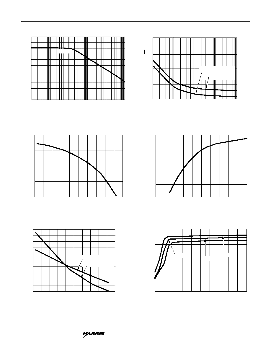
Typical Performance Curves
T
A
= 25
o
C, V
SUPPLY
=
±
15V, R
L
= 1k
, C
L
< 10pF, Unless Otherwise Specified
FIGURE 1. FREQUENCY RESPONSE FOR VARIOUS GAINS
FIGURE 2. GAIN BANDWIDTH PRODUCT vs SUPPLY VOLTAGE
FIGURE 3. GAIN BANDWIDTH PRODUCT vs TEMPERATURE
FIGURE 4. CMRR vs FREQUENCY
100
80
60
40
20
0
GAIN (dB)
0
90
180
PHASE (DEGREES)
1K
10K
100K
1M
10M
FREQUENCY (Hz)
OPEN LOOP
A
VCL
= 1000
A
VCL
= 100
A
VCL
= 10
OPEN LOOP
100M
650
600
550
500
5
6
7
8
9
10
11
12
13
14
15
SUPPLY VOLTAGE (
±
V)
GAIN B
AND
WIDTH PR
ODUCT (MHz)
750
650
550
450
350
250
-60
-40
-20
0
20
40
60
80
100
120
140
TEMPERATURE (
o
C)
GAIN B
AND
WIDTH PR
ODUCT (MHz)
100
10K
100K
1M
10M
FREQUENCY (Hz)
1K
90
80
70
60
50
40
30
20
CMRR (dB)
HA-2840
5
FIGURE 5. PSRR vs FREQUENCY
FIGURE 6. INPUT NOISE vs FREQUENCY
FIGURE 7. SLEW RATE vs TEMPERATURE
FIGURE 8. SLEW RATE vs SUPPLY VOLTAGE
FIGURE 9. INPUT OFFSET VOLTAGE AND INPUT BIAS
CURRENT vs TEMPERATURE
FIGURE 10. SUPPLY CURRENT vs SUPPLY VOLTAGE
Typical Performance Curves
T
A
= 25
o
C, V
SUPPLY
=
±
15V, R
L
= 1k
, C
L
< 10pF, Unless Otherwise Specified (Continued)
100
10K
100K
1M
10M
FREQUENCY (Hz)
1K
100
90
80
70
60
50
40
30
20
10
0
110
PSRR (dB)
±
PSRR
10
100
1K
10K
100K
FREQUENCY (Hz)
NOISE V
O
L
T
A
GE (nV/
Hz)
NOISE CURRENT (pA/
Hz)
NOISE CURRENT
NOISE VOLTAGE
50
37.5
25
12.5
0
30
20
10
0
750
700
650
600
550
SLEW RA
TE (V/
µ
s)
-60
-40
-20
0
20
40
60
80
100
120
140
TEMPERATURE (
o
C)
700
650
600
550
500
450
5
6
7
8
9
10
11
12
13
14
15
SUPPLY VOLTAGE (
±
V)
SLEW RA
TE (V/
µ
s)
8.0
7.0
6.0
5.0
4.0
3.0
INPUT BIAS CURRENT (
µ
A)
3.5
2.5
1.5
0.5
-0.5
INPUT OFFSET V
O
L
T
A
GE (mV)
-60
-40 -20
0
20
40
60
80
100
120 140
TEMPERATURE (
o
C)
BIAS CURRENT
OFFSET VOLTAGE
25
o
C
5
6
7
8
9
10
11
12
13
14
15
14
12
10
8
6
SUPPLY VOLTAGE (
±
V)
SUPPL
Y CURRENT (mA)
-55
o
C
125
o
C
HA-2840
6
FIGURE 11. POSITIVE OUTPUT SWING vs TEMPERATURE
FIGURE 12. NEGATIVE OUTPUT SWING vs TEMPERATURE
FIGURE 13. MAXIMUM UNDISTORTED OUTPUT SWING vs
FREQUENCY
FIGURE 14. TOTAL HARMONIC DISTORTION vs FREQUENCY
FIGURE 15. INTERMODULATION DISTORTION vs FREQUENCY (TWO TONE)
Typical Performance Curves
T
A
= 25
o
C, V
SUPPLY
=
±
15V, R
L
= 1k
, C
L
< 10pF, Unless Otherwise Specified (Continued)
15
10
5
2.5
POSITIVE OUTPUT SWING (V)
-60
-40
-20
0
20
40
60
80
100
120
140
TEMPERATURE (
o
C)
12.5
7.5
0
±
15V, 1k
±
15V, 150
±
15V, 75
±
8V, 1k
±
8V, 150
±
8V, 75
-12.5
-10
-7.5
-5
-2.5
OUTPUT SWING (V)
-60
-40
-20
0
20
40
60
80
100
120
140
TEMPERATURE (
o
C)
±
8V, 75
±
8V, 150
±
8V, 1k
±
15V, 75
±
15V, 150
±
15V, 1k
1K
10K
100K
1M
10M
100M
FREQUENCY (Hz)
25
20
15
10
5
0
V
SUPPLY
=
±
8V
V
SUPPLY
=
±
15V
OUTPUT V
O
L
T
A
GE SWING (V
P-P
)
100K
1M
10M
FREQUENCY (Hz)
-85
-75
-65
-55
-45
-35
THD (dBc)
V
O
= 10V
P-P
V
O
= 1V
P-P
V
O
= 2V
P-P
V
O
= 0.5V
P-P
-95
-85
-75
-65
-55
-45
-35
500K
1M
10M
FREQUENCY (Hz)
THIRD INTERMOD PR
ODUCT (dBc)
V
O
= 5V
P-P
V
O
= 0.5V
P-P
V
O
= 0.25V
P-P
V
O
= 2V
P-P
V
O
= 1V
P-P
HA-2840
7
Die Characteristics
DIE DIMENSIONS:
65 mils x 52 mils x 19 mils
1650
µ
m x 1310
µ
m x 483
µ
m
METALLIZATION:
Type: Aluminum, 1% Copper
Thickness: 16k
≈
±
2k
≈
PASSIVATION:
Type: Nitride over Silox
Silox Thickness: 12k
≈
±
2k
≈
Nitride thickness: 3.5k
≈
±
1k
≈
SUBSTRATE POTENTIAL (Powered Up):
V-
TRANSISTOR COUNT:
34
PROCESS:
High Frequency Bipolar Dielectric Isolation
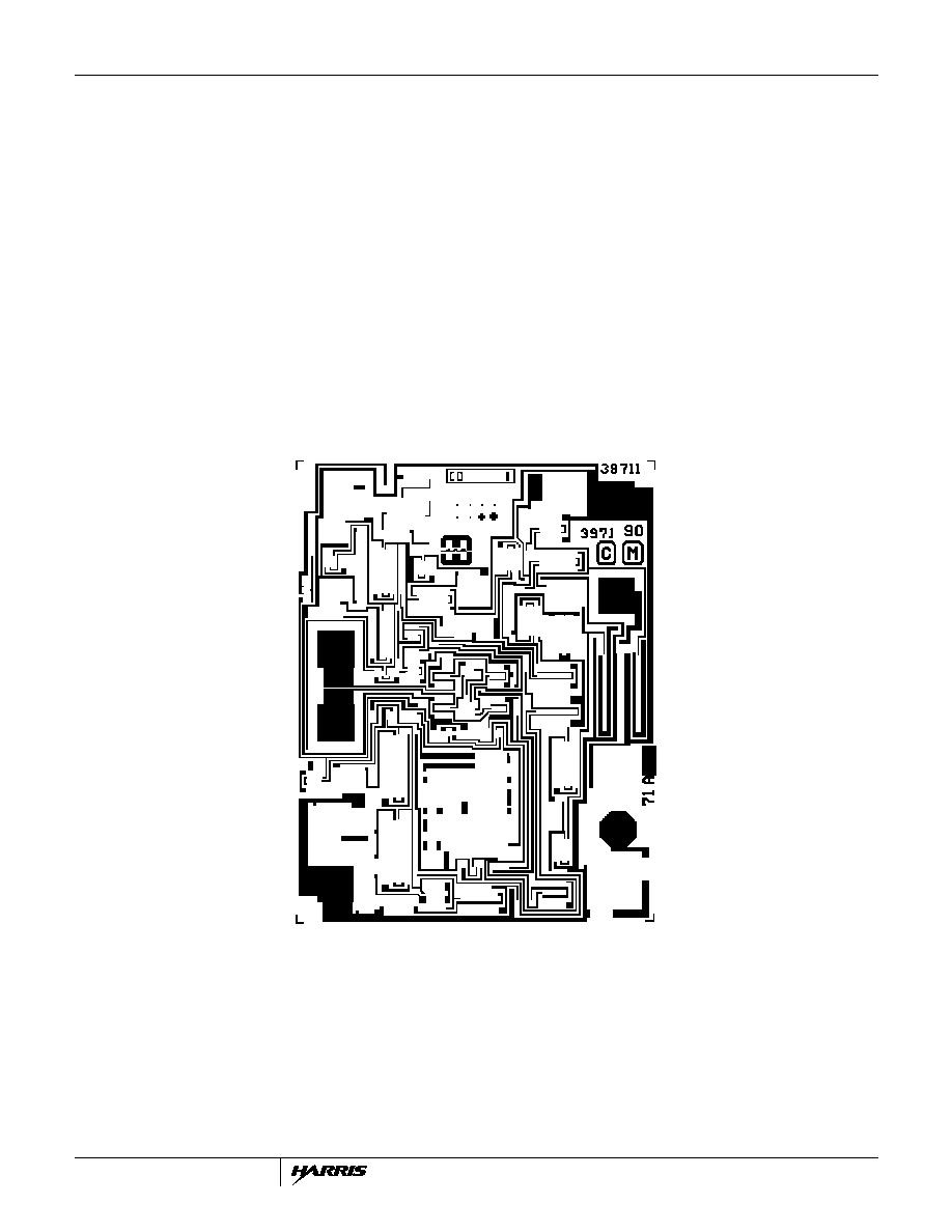
Metallization Mask Layout
HA-2840
V-
+IN
-IN
OUT
V+
HA-2840