 | –≠–ª–µ–∫—Ç—Ä–æ–Ω–Ω—ã–π –∫–æ–º–ø–æ–Ω–µ–Ω—Ç: HFA5253CB | –°–∫–∞—á–∞—Ç—å:  PDF PDF  ZIP ZIP |
89
Semiconductor
CAUTION: These devices are sensitive to electrostatic discharge; follow proper IC Handling Procedures.
Copyright
©
Harris Corporation 1998
HFA5253
800MHz, Ultra High-Speed Monolithic Pin
Driver
The HFA5253 is a very high speed monolithic pin driver
solution for high performance test systems. The device will
switch at high data rates between two input voltage levels
providing variable amplitude pulses. Slew Rate Control pins
provide independent control over positive and negative slew
rate allowing the customer to optimize the pin driver speed
for their application. The output impedance is trimmed to
achieve a precision 50
source for impedance matching.
Two differential ECL/TTL compatible inputs control the
operation of the HFA5253, one controlling the V
HIGH
/V
LOW
switching and the other controlling the output's high-
impedance state. The HFA5253's 800MHz data rate makes it
compatible with today's high-speed VLSI test systems and
the +8V to -3V output swing satisfies the most stringent
testing requirements of all common logic families.
The HFA5253 is manufactured in Harris' proprietary
complementary bipolar UHF-1 process.
Features
∑ High Digital Data Rate . . . . . . . . . . . . . . . . . . . . . 800MHz
∑ Very Fast Rise/Fall Times. . . . . . . . . . . . . . . . . . . . . 500ps
∑ Wide Output Range . . . . . . . . . . . . . . . . . . . . . +8V to -3V
∑ Precise 50
Output Impedance
∑ High Impedance, Three-State Output Control
∑ Slew Rate Control
Applications
∑ IC Tester Pin Electronics
∑ Pattern Generators
∑ Pulse Generators
∑ Level Comparator/Translator
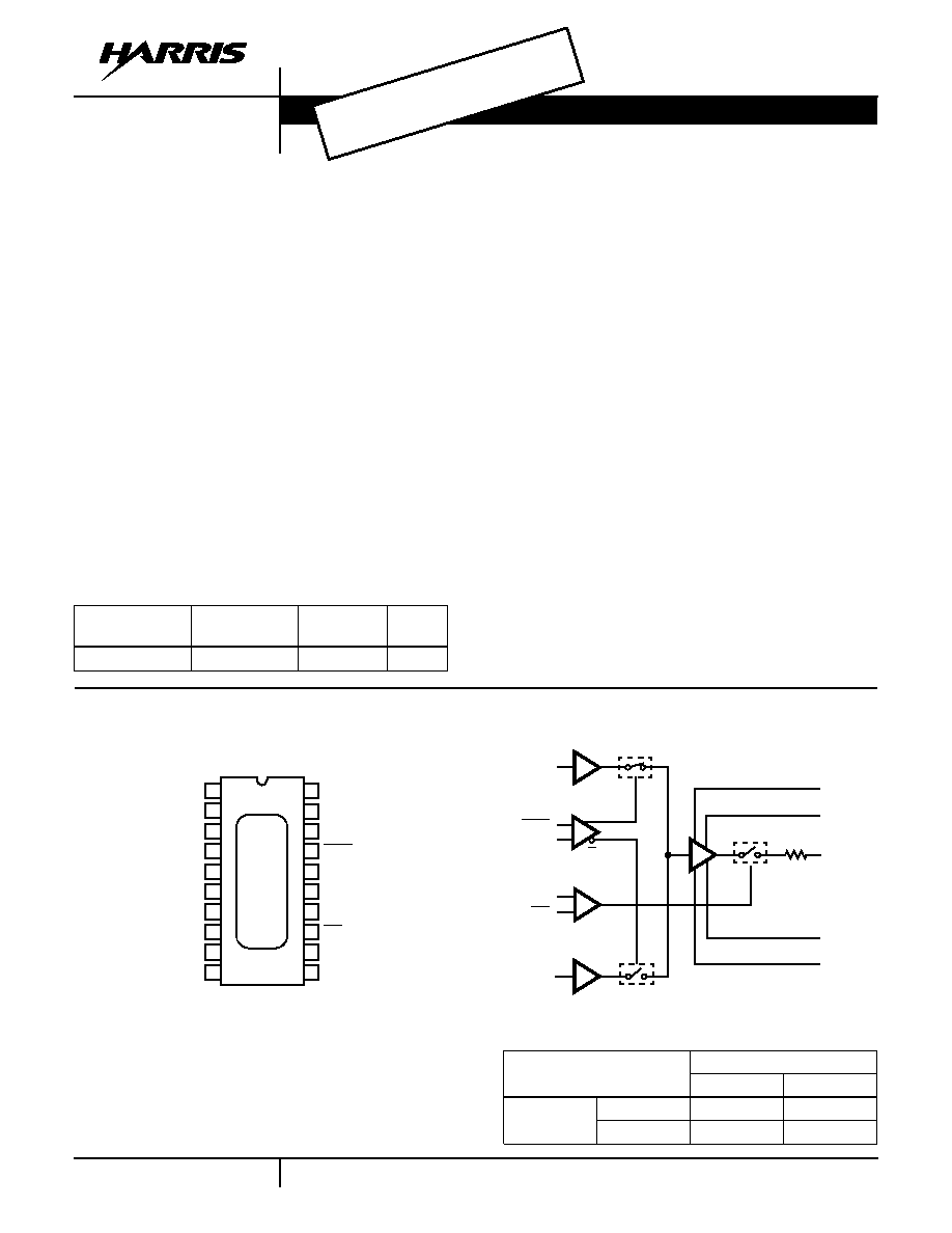
Pinout
HFA5253 (PSOP)
TOP VIEW
Block Diagram
Part Number Information
PART NUMBER
TEMP. RANGE
(
o
C)
PACKAGE
PKG.
NO.
HFA5253CB
0 to 50
20 Ld PSOP
M20.3A
11
12
13
14
15
16
17
18
20
19
10
9
8
7
6
5
4
3
2
1
V
CC1
V
CC1
V
CC2
V
CC2
V
OUT
NC
V
EE2
V
EE2
V
EE1
V
EE1
V
HIGH
NC
DATA
DATA
+SRC
NC
HIZ
HIZ
-SRC
V
LOW
POWER PSOP PACKAGE
(HEAT SLUG SURFACE IS ELECTRICALLY FLOATING)
TRUTH TABLE FOR V
OUT
DATA
0
1
HIZ
0
V
LOW
V
HIGH
1
HIZ
HIZ
INPUT BUFFER
INPUT BUFFER
50
Q
Q
V
HIGH
DATA
DATA
HIZ
HIZ
V
LOW
V
OUT
V
CC
V
EE
+SRC
-SRC
+
-
+
-
October 1998
File Number
4003.4
OBS
OLE
TE P
ROD
UCT
No R
ecom
men
ded
Rep
lace
men
t

90
Pin Descriptions
NAME
FUNCTION
V
CC1
Positive Supply. Nominal value is 11.2V
±
0.2V. Reducing supply voltage below 11.0V will reduce positive output voltage swing.
The total supply voltage from V
CC1
to V
EE1
should not exceed 18.0V for normal operation or exceed 19.0V to prevent damage.
Harris recommends two wire bonds to this pad to provide the lowest possible impedance. In addition, power supply decoupling
chip capacitors of 470pF, 0.1
µ
F and a 10
µ
F tantalum are recommended. Do not connect the V
CC1
and V
CC2
pins together im-
mediately, rather run separate traces until they can be joined at a large bypass capacitor (0.1
µ
F || 10.0
µ
F).
V
EE1
Negative Supply. Nominal value is -6.4V
±
0.2V. A supply voltage more positive than -6.2V will reduce negative output voltage
swing. The total supply voltage from V
CC1
to V
EE1
should not exceed 18.0V for normal operation or exceed 19.0V to prevent
damage. Harris recommends two wire bonds to this pad to provide the lowest possible impedance. In addition, power supply de-
coupling chip capacitors of 470pF, 0.1
µ
F and a 10
µ
F tantalum are recommended. Do not connect the V
EE1
and V
EE2
pins to-
gether immediately, rather run separate traces until they can be joined at a large bypass capacitor (0.1
µ
F || 10.0
µ
F).
V
CC2
Output Stage Positive Supply. Nominal voltage and cautions are the same as for V
CC1
. Having decoupling chip capacitors close
to V
CC2
and V
EE2
is essential since large AC current will flow through this pad to the output during transients. Harris recommends
two wire bonds for this pad. Do not connect the V
CC1
and V
CC2
pins together immediately, rather run separate traces until they
can be joined at a large bypass capacitor (0.1
µ
F || 10.0
µ
F).
V
EE2
Output Stage Negative Supply. Nominal voltage and cautions are the same as for V
EE1
. Having decoupling chip capacitors close
to V
CC2
and V
EE2
is essential since large AC current will flow through this pad to the output during transients. Harris recommends
two wire bonds for this pad. Do not connect the V
EE1
and V
EE2
pins together immediately, rather run separate traces until they
can be joined at a large bypass capacitor (0.1
µ
F || 10.0
µ
F).
V
HIGH
Input Voltage High is used to set the output high level V
OH
. V
HIGH
is sensitive to capacitively coupled AC noise. Protection from
high frequency noise can be achieved with a low pass filter consisting of a 50
chip resistor and a 470pF chip capacitor. Without
this precaution the pin driver may oscillate due to feedback from the output through the PC board ground.
V
LOW
Input Voltage Low is used to set the output low level V
OL
. V
LOW
is sensitive to capacitively coupled AC noise. Protection from
high frequency noise can be achieved with a low pass filter consisting of a 50
chip resistor and a 470pF chip capacitor. Without
this precaution the pin driver may oscillate due to feedback from the output through the PC board ground.
V
OUT
Driver Output. The output impedance has been laser trimmed to match a 50
transmission line
±
2
. Custom output impedance
trimming is available (contact sales office for details) to provide the best match possible to your 50
system.
DATA, DATA
Differential Digital Inputs used to switch V
OUT
to the V
HIGH
or V
LOW
level. Harris recommends this input pair be driven by com-
plementary ECL signals to provide optimal switching speeds and timing accuracy. However a large Common Mode and Differen-
tial Voltage Range is provided to accommodate a variety of signals including single ended TTL and CMOS. When using single
ended signals the other input must be tied to an appropriate threshold voltage.
HIZ, HIZ
Differential Digital Inputs used to switch V
OUT
from an Active to a High Impedance State. Harris recommends that this input pair
be driven by complementary ECL signals to provide optimal switching speeds and timing accuracy. However a large Common
Mode and Differential Voltage Range is provided to accommodate a variety of signals including single ended TTL and CMOS.
When using single ended signals the other input must be tied to an appropriate threshold voltage.
+SRC
The Positive Slew Rate Control Pin adjusts the rising edge slew rate with an external current I
STEAL
. I
STEAL
draws current (0mA
to 10mA) from an internal current source limiting the rate of change of the high impedance node. Typically an external resistor to
GND is sufficient to set the slew rate at a desired level. Leaving the +SRC Pin open will give the highest speed performance. The
external current I
STEAL
for a resistor R
STEAL
connected from +SRC to GND may be calculated by: I
STEAL
= (V
CC
- 0.35)/R
STEAL
.
-SRC
The Negative Slew Rate Control Pin adjusts the falling edge slew rate with an external current I
STEAL
. I
STEAL
supplies current
(0mA to 10mA) to an internal current source limiting the amount of current being drawn from the circuit and thus limiting the rate
of change of the high impedance node. Typically an external resistor to GND is sufficient to set the slew rate at a desired level.
Leaving the -SRC Pin open will give the highest speed performance. The external current I
STEAL
for a resistor R
STEAL
connected
from -SRC to GND may be calculated by: I
STEAL
= (V
EE
+ 0.35)/R
STEAL
.
HFA5253
91
Absolute Maximum Ratings
Thermal Information
Supply Voltage . . . . . . . . . . . . . . . . . . . . . . . . . . . . . . . . . . . . . . 19V
Differential Input Voltage (DATA and HIZ) . . . . . . . . . . . . . . . . . . 5V
Output Current Continuous (Note 1) . . . . . . . . . . . . . . . . . . . 160mA
Input Voltage (Any pin except as specified) . . . . . . . . . . V
CC
to V
EE
V
OUT
Voltage (Note 3) . . . . . . . . . . . . . . . . . . . . . . . . . . . . 9V to -4V
V
HIGH
Voltage . . . . . . . . . . . . . . . . . . . . . . . . . . . . . . . . V
CC
to -4V
V
LOW
Voltage . . . . . . . . . . . . . . . . . . . . . . . . . . . . . . . . . 9V to V
EE
V
HIGH
to V
LOW
Voltage . . . . . . . . . . . . . 11V to 0V (V
HIGH
> V
LOW
)
Slew Rate Control Current (+SRC, -SRC) . . . . . . . . . . . . . . . . 12mA
Operating Conditions
Temperature Range . . . . . . . . . . . . . . . . . . . . . . . . . . . 0
o
C to 50
o
C
Thermal Resistance (Typical, Note 2)
JA
(
o
C/W)
JC
(
o
C/W)
20 Ld PSOP Package . . . . . . . . . . . . .
49
2
(
JC
Measured At Copper Slug Top Center with Infinite Heat Sink)
Maximum Junction Temperature (Die) . . . . . . . . . . . . . . . . . . . 175
o
C
Maximum Junction Temperature (Plastic Package) . . . . . . . 150
o
C
Maximum Storage Temperature Range . . . . . . . . . . -65
o
C to 150
o
C
Maximum Lead Temperature (Soldering 10s) . . . . . . . . . . . . 300
o
C
(PSOP - Lead Tips Only)
CAUTION: Stresses above those listed in "Absolute Maximum Ratings" may cause permanent damage to the device. This is a stress only rating and operation of the
device at these or any other conditions above those indicated in the operational sections of this specification is not implied.
NOTES:
1. Internal Power Dissipation may limit Output Current below 160mA.
2.
JA
is measured with the component mounted on an evaluation PC board in free air.
3. Shorting the output to a voltage outside the specified range may damage the output.
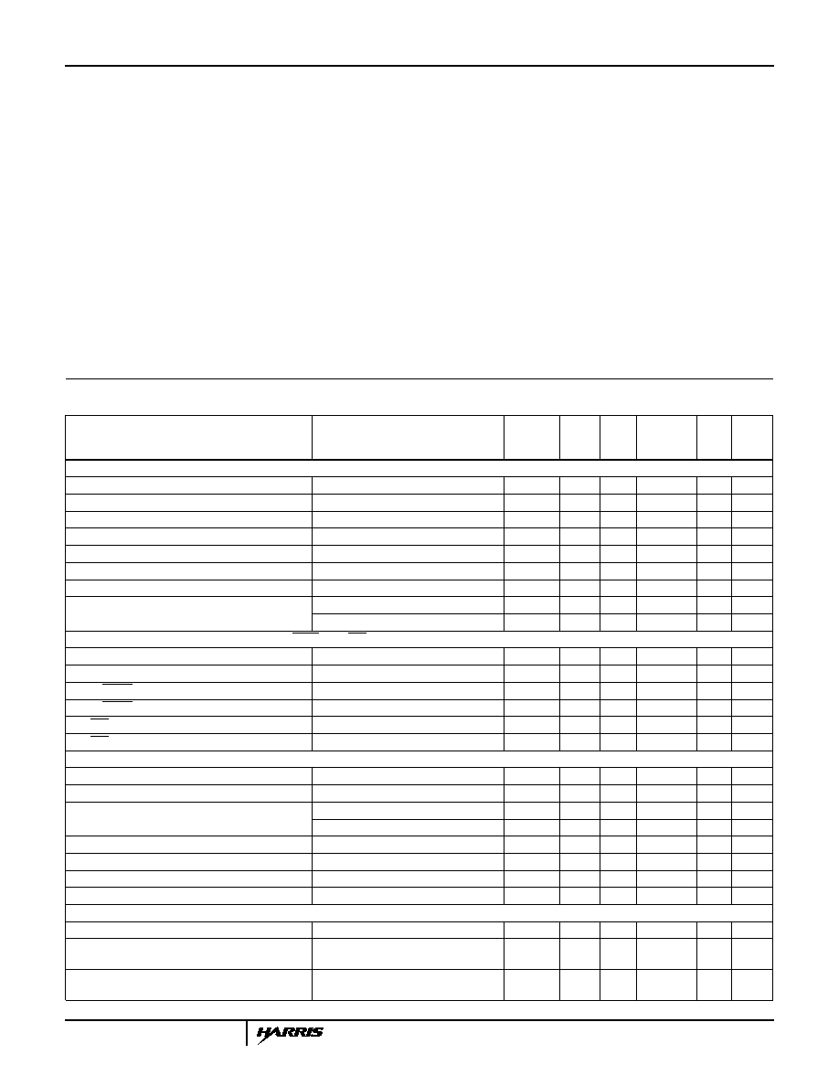
Electrical Specifications
V
CC
= +11.2V; V
EE
= -6.4V; V
IH
= -0.9V; V
IL
= -1.75V; +SRC and -SRC are Not Connected, Unless
Otherwise Specified
PARAMETER
TEST CONDITIONS
(NOTE 4)
TEST
LEVEL
TEMP.
(
o
C)
MIN
TYP
MAX UNITS
INPUT CHARACTERISTICS (V
HIGH
, V
LOW
)
V
HIGH
Input Offset Voltage
A
25
-150
-50
+50
mV
V
LOW
Input Offset Voltage
A
25
-150
-50
+50
mV
V
HIGH
Input Bias Current
V
HIGH
= -3.25V to +8.5V
A
25
-50
110
400
µ
A
V
LOW
Input Bias Current
V
LOW
= -3.5V to +8.25V
A
25
-400
-110
50
µ
A
V
HIGH
Voltage Range
A
25
-3.5
-
8.5
V
V
LOW
Voltage Range
A
25
-3.5
-
8.5
V
V
HIGH
to V
LOW
Differential Voltage Range
V
HIGH
V
LOW
A
25
0
-
9.5
V
V
HIGH
/V
LOW
Interaction (Notes 5, 17)
At 500mV
A
25
-
2
4
mV
At 250mV
A
25
-
20
40
mV
LOGIC INPUT CHARACTERISTICS (DATA, DATA, HIZ, HIZ)
Logic Input Voltage Range
B
25
-3
-
8
V
Logic Differential Input Voltage
B
25
0.4
-
5
V
DATA/DATA Logic Input High Current
V
IH
= 0V, V
IL
= -2V
A
25
-50
110
700
µ
A
DATA/DATA Logic Input Low Current
V
IH
= 0V, V
IL
= -2V
A
25
-700
-300
50
µ
A
HIZ/HIZ Logic Input High Current
V
IH
= 0V, V
IL
= -2V
A
25
-50
70
400
µ
A
HIZ/HIZ Logic Input Low Current
V
IH
= 0V, V
IL
= -2V
A
25
-400
-80
50
µ
A
TRANSFER CHARACTERISTICS
V
HIGH
Voltage Gain
V
HIGH
= -1V to 6.5V
A
25
0.95
0.97
1
V/V
V
LOW
Voltage Gain
V
LOW
= -1.5V to 6V
A
25
0.95
0.97
1
V/V
V
HIGH
/V
LOW
Linearity Error
Fullscale = 5V, Note 6
A
25
-0.1
-
0.1
%
Fullscale = 10.5V, Note 7
A
25
-0.8
-
0.8
%
V
HIGH
/V
LOW
-3dB Bandwidth
200mV
P-P
B
25
-
100
-
MHz
Typical Slew Rate Control Range
I
STEAL
= 0mA to 10mA, 5V Step
B
25
1.0
-
2.8
V/ns
+SRC Pin Voltage
C
25
-
V
CC
- 0.35
-
V
-SRC Pin Voltage
C
25
-
V
EE
+ 0.35
-
V
SWITCHING CHARACTERISTICS (Z
LOAD
= 16 inches of RG-58 Terminated with 50
)
Propagation Delay (Notes 8, 10)
B
25
1
-
2
ns
Propagation Delay Match (Rising to Falling Edge,
Notes 8, 10)
B
25
-100
-
100
ps
Rising Edge Propagation Delay vs Duty Cycle
(Notes 9, 10)
B
25
-120
-20
80
ps
HFA5253

92
Falling Edge Propagation Delay vs Duty Cycle
(Notes 9, 10)
B
25
-80
20
120
ps
Active to HIZ Delay (Note 10)
B
25
1.5
2.0
2.5
ns
HIZ to Active Delay (Note 10)
B
25
2.8
3.3
3.8
ns
TRANSIENT RESPONSE (Z
LOAD
= 16 inches of RG-58 Terminated with 5pF)
Rise/Fall Time
1V
P-P
, 20% - 80% (Note 11)
B
25
350
450
500
ps
3V
P-P
, 10% - 90% (Note 11)
B
25
700
890
1000
ps
5V
P-P
, 10% - 90% (Note 12)
B
25
1.1
1.3
1.7
ns
Rise/Fall Time Match (Note 12)
B
25
-
100
-
ps
Minimum Output Pulse Width (Note 13)
1V
P-P
B
25
-
1.0
-
ns
3V
P-P
B
25
-
1.2
-
ns
5V
P-P
B
25
-
2.0
-
ns
Overshoot/Undershoot/Preshoot
3V
P-P
B
25
-
5
-
%
Data Settling Time (Note 14)
To 1%
B
25
-
10
-
ns
OUTPUT CHARACTERISTICS
Output Voltage Swing
No Load
at
V
CC
= 11V, V
EE
= -6.2V
A
25
-3
-
8
V
Output Amplitude Voltage
V
OH
- V
OL
A
25
0.25
-
9.0
V
DC Output Resistance (Note 15)
-3V to 8V
A
25
45
47
49
Output Leakage - HIZ
-3V to 8V
A
25
-100
-
100
nA
Output Capacitance - HIZ
C
25
-
5
-
pF
Output Current - Active
A
25
80
100
-
mA
Output Short Circuit Range (Note 3)
A
25
-4.0
-
9.0
V
POWER SUPPLY CHARACTERISTICS (V
HIGH
= 5V Active, No Load)
V
HIGH
Power Supply Rejection Ratio (Note 16)
A
25
-
14
40
mV/V
V
LOW
Power Supply Rejection Ratio (Note 16)
A
25
-
14
40
mV/V
Total Supply Current
A
25
90
96
98
mA
I
CC1
/I
EE1
Supply Current
B
25
-
74
-
mA
I
CC2
/I
EE2
Supply Current
B
25
-
22
-
mA
Supply Voltage Range
V
CC
A
25
11.0
11.2
11.4
V
V
EE
A
25
-6.6
-6.4
-6.2
V
V
CC
- V
EE
A
25
17.2
-
18.0
V
Power Dissipation
V
CC
= 11.2V, V
EE
= -6.4V, No Load
A
25
-
-
1.72
W
NOTES:
4. Test Level: A = 100% production tested, B = Typical or limit based on lab characterization of a limited number of lots, C = Design Information,
goal or condition.
5. V
HIGH
to V
LOW
Interaction is measured as the change in V
OUT
(the active channel) due to a change in the inactive channel. V
HIGH
Interaction
at 250mV is measured as the deviation from 1V as V
LOW
is changed from 0V to 750mV (Referred to V
OUT
). V
LOW
Interaction at 250mV is
measured as the deviation from 0V as V
HIGH
is changed from 1V to 250mV (Referred to V
OUT
).
6. For V
HIGH
= 0V to 5V, for V
LOW
= 0V to 5V, Fullscale = 5V, 0.1% = 5mV. Output Amplitude (V
HIGH
- V
LOW
) = 1V
P-P
.
7. For V
HIGH
= -2.5V to 8V, for V
LOW
= -3.0V to 7.5V, Fullscale = 10.5V, 0.1% = 10.5mV. Output Amplitude (V
HIGH
- V
LOW
) = 1V
P-P.
8. 3V Step, 50% duty cycle, 200ns period.
9. 0V to 3V Step, 200ns period, Pulse Width is varied from 5ns to 195ns.
10. Test is performed into a 50
load with a 3V step. Measurement is made from the 50% of the input to 50% of output.
11. Limit based on calculation.
12. 5V Step, 50% duty cycle, 100ns period.
13. Minimum Pulse Width is measured 50% to 50% of specified amplitude with pulse peak at 100% of amplitude.
14. 3V Step, measured from 50% of input to
±
1% of reference value at 50ns.
15. Dynamic Output Resistance will be higher (Typ 48.5
) than DC Output Resistance. DC Output Resistance is measured at 0V with I
OUT
set
from 0mA to 40mA.
16. V
HIGH
= 2.6V, V
LOW
= 2.3V, V
CC
= 10.2V to 11.2V, V
EE
= -5.4V to -6.4V.
17. Input voltages V
HIGH
and V
LOW
are corrected for Offset Voltage and Gain Error.
Electrical Specifications
V
CC
= +11.2V; V
EE
= -6.4V; V
IH
= -0.9V; V
IL
= -1.75V; +SRC and -SRC are Not Connected, Unless
Otherwise Specified (Continued)
PARAMETER
TEST CONDITIONS
(NOTE 4)
TEST
LEVEL
TEMP.
(
o
C)
MIN
TYP
MAX UNITS
HFA5253
93
Functional Block Diagram
The HFA5253 functional block diagram is shown in on the first
page of this data sheet.
The control inputs, DATA and DATA, determine the output level.
If DATA is at logic "1" and DATA is at logic "0", the output level
will be the same as V
HIGH
. If DATA is at logic "0" and DATA is at
logic "1", the output will be the same as V
LOW
. The control
inputs, HIZ and HIZ, cause the output to become either active
or high-impedance. If HIZ is at logic "1" and HIZ is at logic "0",
the output will be in high impedance mode. If HIZ is at logic "0"
and HIZ is at logic "1", the output will be enabled. The output
impedance in the enabled mode is trimmed to 50
.
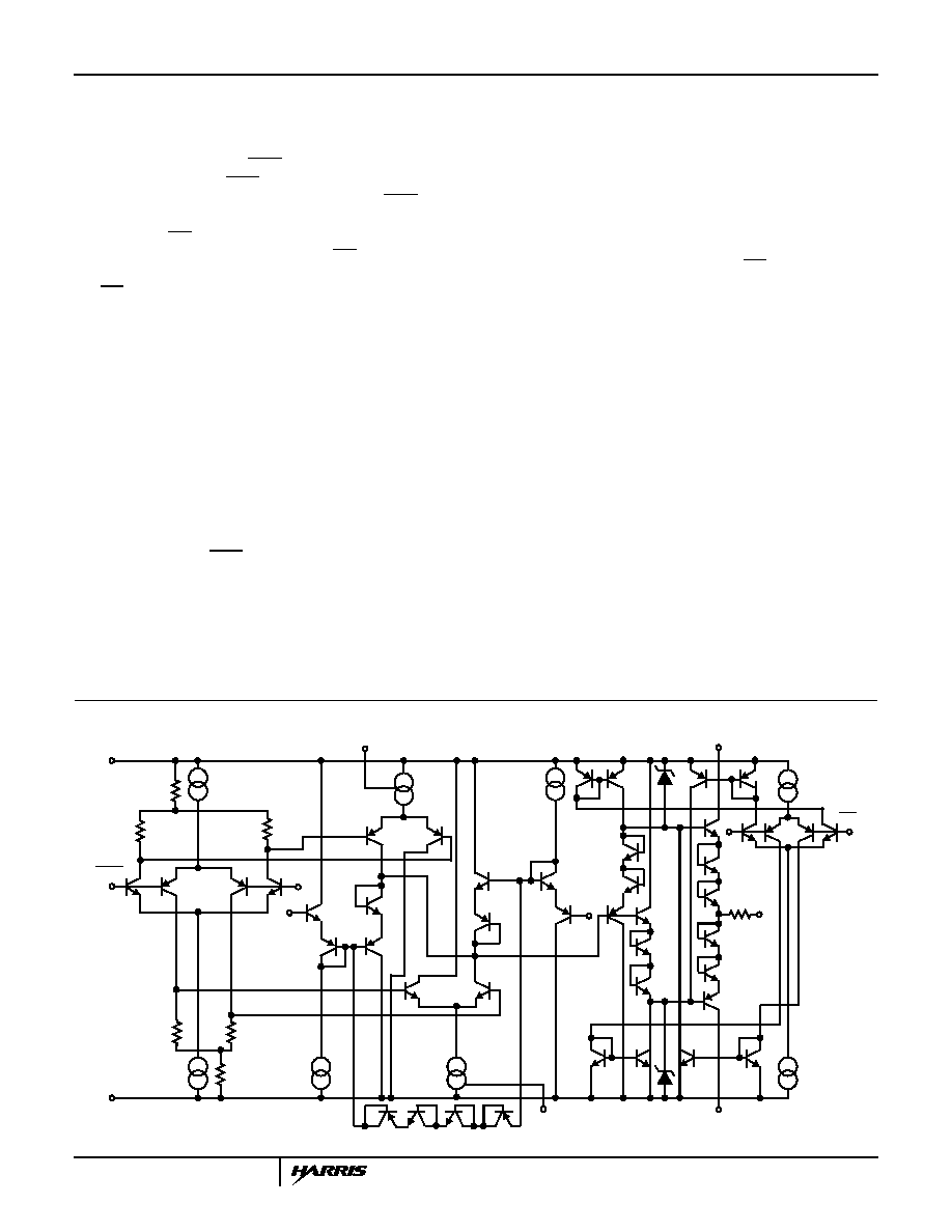
Circuit Schematic
The Pin Driver circuit consists of a switch, an output buffer,
and two differential control elements as shown in the circuit
Schematic Diagram.
A two stage approach, separating the switch from the output
buffer, allows the speed and accuracy requirements of the
switch to be de-coupled from the load driving capability of
the buffer.
The patented switch circuitry [3] uses cascaded emitter
followers as input buffers and also to switch the input V
HIGH
and V
LOW
to node VSO. Dual differential pairs controlled by the
data timing (DATA and DATA) direct current to select either the
V
HIGH
or V
LOW
switch. Matching transistor types and
transdiodes improve linearity and lowers the voltage offset and
offset drift. Stacking two emitter-base junctions allows the
V
HIGH
to V
LOW
range to be extended to two Emitter - Base
breakdown voltages of the process. The speed of the pin driver
is largely determined by the current flowing through the switch
stage and the collector-base capacitance of the output stage
transistors connected to the node VSO. The Slew Rate Control
Pins, +SRC and -SRC, allow the user to control the amount of
current available in the V
HIGH
and V
LOW
switch, respectively
and thus the slew rate of node VSO.
The output stage consists of cascaded emitter followers
constructed in a typical push-pull manner as shown in the
Schematic Diagram. However, transdiodes are added to
increase the voltage breakdown characteristics of the output
during high impedance mode. HIZ and HIZ control the mode
of the output stage. A trimmed, NiCr resistor is added to
provide the 50
output impedance.
Overall, a symmetry of device types and paths is constructed
to improve slew and delay symmetry. Both the V
HIGH
to V
OUT
path and the V
LOW
to V
OUT
path contain three NPN and
three PNP transistors operating at similar collector currents.
Thus the transient response of V
HIGH
to V
LOW
and V
LOW
to
V
HIGH
are kept symmetrical. Also, a trimmable current
reference (not shown) allows the AC parameters to be
adjusted to maintain unit to unit consistency.
Application Information
The HFA5253 is a pin driver designed for use in automatic
test equipment (ATE) and high speed pulse generators. Pin
drivers, especially those with very high-speed performance,
have generally been implemented with discrete transistors
(sometimes GaAs) on a circuit board or in a hybrid. Recent
IC process improvements, specifically Harris' UHF1 process
[2], have enabled the manufacturing of the 500MHz and
800MHz silicon monolithic pin drivers, HFA5250, HFA5251
and now the HFA5253.
Schematic Diagram
V
CC1
V
EE1
DATA
DATA
V
HIGH
V
LOW
VSO
V
OUT
HIZ
HIZ
V
CC2
V
EE2
HIZ CONTROL
OUTPUT STAGE
SWITCHING STAGE
V
HIGH
/V
LOW
CONTROL
+SRC
-SRC
HFA5253

94
The ultra high speed performance of the HFA5253 is a result
of UHF1 process leverages: low parasitic collector-to-
substrate capacitance of the bonded wafer, low collector-to-
base parasitic capacitance of the self-aligned base/emitter
technology and ultra high f
T
NPN (8GHz) and PNP (5.5GHz)
poly-silicon transistors.
Definition of Terms
V
OH
AND V
OL
Output High Voltage and Output Low Voltage. V
OH
is the
voltage at V
OUT
when the HIZ input is low and the DATA
input is high. V
OL
is the voltage at V
OUT
when HIZ is low and
DATA is low. The V
OH
and V
OL
levels are set with the V
HIGH
and V
LOW
inputs respectively.
OFFSET VOLTAGE
Offset Voltage is the DC error between the voltage placed on
V
HIGH
or V
LOW
and the resulting V
OH
and V
OL
. V
HIGH
Offset Voltage Error is obtained by measuring V
OH
with
V
HIGH
set to 0V and V
LOW
set to -2.5V to minimize
interaction effects. V
LOW
Offset Voltage Error is the
measurement of V
OL
with V
LOW
set to 0V and V
HIGH
set to
+7.5V.
GAIN
Gain is defined as the ratio of output voltage change to
input voltage change for a defined range. V
HIGH
Gain is
calculated with the following equation with V
LOW
fixed at
-2.5V:
V
LOW
Gain is calculated in a similar manner:
V
HIGH
is held fixed at 7.5V. These Gain calculations minimize
the effects of Interaction and End Point Nonlinearities.
LINEARITY ERROR
Linearity Error is a measure of output voltage worst case
deviation from a straight line that has been corrected for
offset and 7.5V Gain. Linearity Error is given as a
percentage of fullscale and is done in two ranges, 5V and
10.5V. DATA is measure at 0.5V steps from -2.5V to 8V for
V
HIGH
and -3V to 7.5V for V
LOW
. The Linearity Error
equation is as follows for 10.5V fullscale:
The Linearity Error equation is as follows for 5V fullscale:
Linearity Error is calculated for every data point in the range
and the worst case value is recorded.
V
HIGH
TO V
LOW
INTERACTION
V
HIGH
to V
LOW
Interaction is the change in V
OUT
(the
active channel) due to the inactive channel. V
HIGH
Interaction is measured as the change in V
OH
from 1V as
V
LOW
is moved from 0V to 750mV (V
LOW
is corrected for
gain and offset errors). V
LOW
Interaction is measured as
the change in V
OL
from 0V as V
HIGH
is moved from 1V to
250mV (with V
HIGH
corrected for gain and offset errors).
The minimum recommended difference between V
HIGH
and V
LOW
for the HFA5253 is 250mV.
Speed Advantage
Harris Pin Drivers on bonded-wafer technology definitely have
a speed advantage, coming from the low collector-to-
substrate capacitance and the high f
T
of the transistors. In
addition, the patented switching stage which fits uniquely to
Harris' UHF1 process is another big contributor for the high
speed. This switching circuitry requires low series-resistance
NPN and PNP transdiodes available in UHF1. The rise and
fall times of the pin driver are largely determined by the slew
rate at the node VSO in the Schematic. The dominant
mechanism for the slew rate is the charging/discharging of the
collector-base capacitors of the transistors connected to the
node VSO. The charging/discharging currents are coming
from the switching stage current sources. The fast rise and fall
times are achieved because of the negligible collector-to-
substrate capacitance and the small base-collector
capacitance due to the self-aligned recessed oxide [2].
The DATA/DATA differential stage is not a factor for the speed if
its current sources have enough current not to bottleneck the
transient. However it should be noted that the propagation
delay mismatch is determined by this stage. Sufficient current is
allocated to the differential stage current sources to best match
the low-to-high and high-to-low transient propagation delays.
The specified load condition is a 16 inch 50
SMA cable with a
5pF capacitor at the end of the cable. This load simulates a
typical ATE environment for a DUT (Device Under Test) with
high impedance (>1k
) digital inputs. The rise/fall time for
HFA5253 with 5V
P-P
is typically 1.3ns. Pin drivers, built out of
the same circuit structure as shown in the Schematic, can be
made faster by trimming for a higher power supply current.
Currently the pin driver has rise/fall times of less than 1ns (10%
to 90% of 5V
P-P
) when I
CC
is trimmed to 125mA. Further
speed enhancement will be made if there is a market demand.
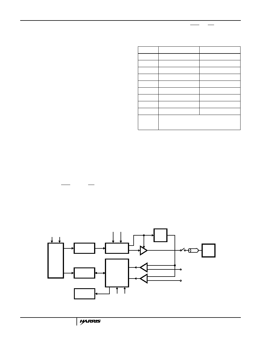
Basic ATE System Application
Figure 1 shows a pin driver in a typical per-pin ATE system. The
pin driver works closely with the Dual-Level Comparator and
the Active Load. When the DUT pin acts as an input waiting for
a series of digital signals, the pin driver becomes active with a
logic "0" applied on the HIZ pin and provides the DUT pin with
digital signals. When the DUT pin acts as an output, the pin
driver output will be in high impedance mode (HIZ) with a logic
V
HIGH
GAIN
V
OH
V
HIGH
at 6.5V
(
)
V
OH
V
HIGH
at -1V
(
)
≠
7.5
------------------------------------------------------------------------------------------------------------------
=
V
LOW
GAIN
V
OL
V
LOW
at 6V
(
)
V
OL
V
LOW
at -1.5V
(
)
≠
7.5
-------------------------------------------------------------------------------------------------------------
=
Linearity Error
V
OUT
V
OUT
IDEAL
(
)
≠
10.5
--------------------------------------------------------------
=
V
OUT
IDEAL
(
)
V
IN
Gain
◊
Offset
+
=
Linearity Error
V
OUT
V
OUT
IDEAL
(
)
≠
5
--------------------------------------------------------------
=
HFA5253
95
"1" applied to the "HIZ" pin. During this high impedance mode
the pin driver presents a capacitance of less than 5pF to the
DUT. Special care has to be taken to match the impedance (to
50
) at the pin driver output to minimize reflections.
The Dual-Level Comparator detects the logic levels of the
DUT pin when it acts as an output. The comparator has two
threshold level inputs, V
CH
and V
CL
. The logic level
information of the DUT pin output is sent to the
edge/window comparator through the Dual-Level
Comparator. The edge/window comparator interprets this
information in terms of corresponding transient
performance in conjunction with the timing information.
Thus it detects any possible failure transients.
The formatter sends a sequence of digital information to the
pin driver which contains logic information over time. The
Active Load is enabled when the DUT pin acts as an output.
It simulates the load of the DUT pin by sinking or sourcing
programmed current. Finally the sequencer controls the
overall activities of the automatic testing.
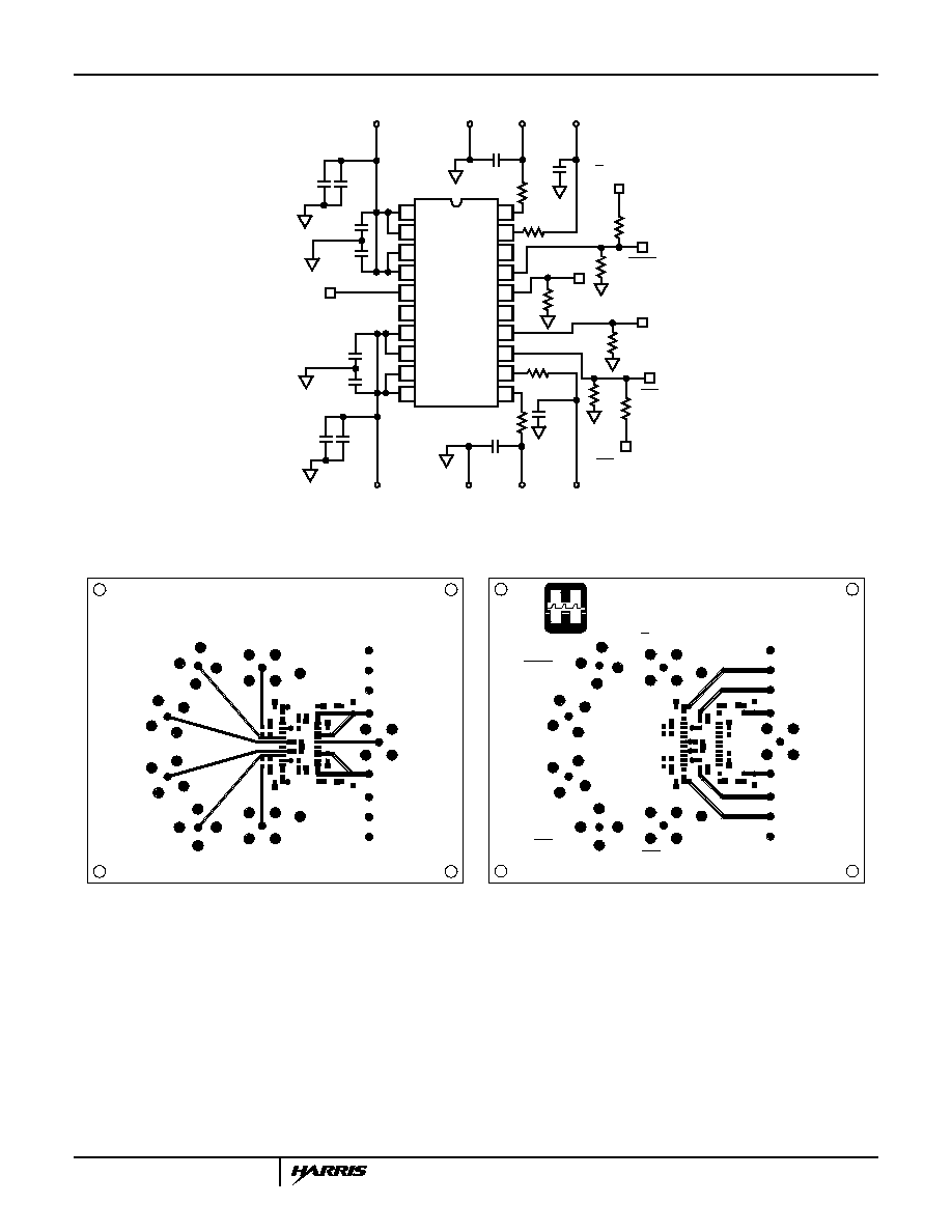
Decoupling Circuit for Oscillation-Free Operation
To ensure oscillation-free operation in ATE or pulse generator
applications, the pin driver needs an appropriate decoupling
circuit on a printed circuit board which consists of chip
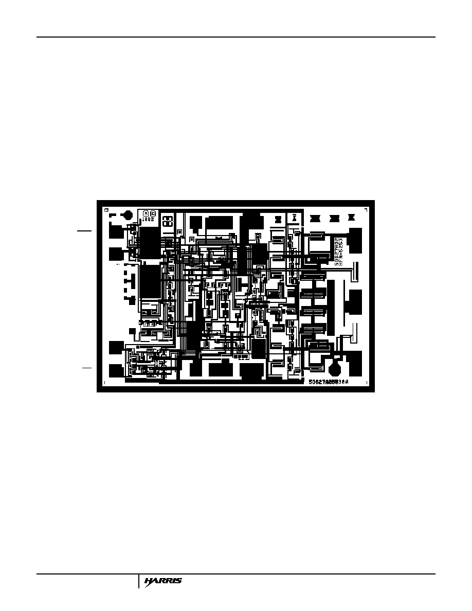
capacitors and chip resistors. Figures 2, 3, and 4 refer to a
proven decoupling circuit currently working in the lab and a 1X
scale film of its associated PC board (metal level). Do not
connect the V
CC1
and V
CC2
pins or the V
EE1
and V
EE2
pins
together immediately, rather run separate traces until they can
be joined at a large bypass capacitor (0.1
µ
F || 10.0
µ
F).
The control pins, DATA, DATA, HIZ, and HIZ are fed ECL
signals through 50
micro-strip lines terminated with 50
for
impedance matching since the input impedance at these
pins is much higher than 50
. At the end of the micro-strip
lines there is usually a high-speed pulse generator with an
output impedance of 50
. A 50
micro-strip line is
connected to each of the pins, DATA and HIZ through a 50
chip resistor to monitor the pulse signals.
The input pins, V
HIGH
, V
LOW
, +SRC, and -SRC need to be
protected from any capacitively coupled AC noise. Normally
this protection can be achieved by having a low pass filter
consisting of a 50
chip resistor and a chip capacitor, 470pF
for V
HIGH
/V
LOW
and 0.1
µ
F for +SRC/-SRC. Without this
protection circuit the pin driver may oscillate due to signals
fed back from the output through the PC board ground.
The power supply pins, V
CC1
, V
CC2
, V
EE1
, and V
EE2
,
require decoupling chip capacitors of 470pF, 0.1
µ
F, 10
µ
F.
Having decoupling capacitors close to V
CC2
and V
EE2
is
essential since large AC current will flow through either
V
CC2
or V
EE2
during transients.
The output of the pin driver is usually connected to the device-
under-test (DUT) through 50
micro-strip line and coaxial cable
which carries the signal to a high input impedance DUT pin.
PARTS LIST
QTY
VALUE
COMPONENT
6
470pF
Chip Cap: 0805
4
0.1
µ
F
Chip Cap: 0805
2
10
µ
F
Tant.
8
50
Chip Res: 0805
2
100
Chip Res: 0805
7
SMA Jacks
Wide Body
1
20 Lead PSOP
HFA5253
4
4-40
1" Standoff
4
4-40
1/4" Screws
2
Twisted Wire Assemblies with 4 Wires Each:
One for V
CC
, V
HIGH
, +SRC, GND; and 1 for V
EE
, V
LOW
,
-SRC, GND.
CLOCK,
START
MEMORY
EDGE/
WINDOW
COMPARATOR
MEMORY
DATA
FORMATTER
FAIL
MEMORY
FAIL
SEQUENCER
TIMING
DATA
TIMING
DUT
DATA
ACTIVE
LOAD
50
V
CH
V
CL
DUAL LEVEL COMPARATOR
PIN DRIVER
HIZ
FIGURE 1. TYPICAL ATE SYSTEM
HFA5253
96
References
[1] Taewon Jung and Donald K. Whitney Jr., "A 500MHz
ATE Pin Driver," Bipolar Circuits and Technology
Meeting Proceedings, pp238-241, October 1992.
[2] Chris K. Davis et. al., "UHF1: A High Speed Complementary
Bipolar Analog Process on SOI," Bipolar Circuits and Tech-
nology Meeting Proceedings, pp260-263, October 1992.
[3] Donald K. Whitney Jr., "Symmetrical, High Speed,
Voltage Switching Circuit," United States Patent
Pending, Filed November 1991.
FIGURE 3. 1X PC BOARD LAYOUT (BOTTOM VIEW)
FIGURE 4. 1X PC BOARD LAYOUT (TOP VIEW)
V
OUT
11
12
13
14
15
16
17
18
20
19
10
9
8
7
6
5
4
3
2
1
HIZ
HIZ-SCOPE
-SRC
100
50
100
50
0.1
µ
F
V
LOW
50
GND
(-6.4V) V
EE
10
µ
F
470pF
470pF
HIZ
0.1
µ
F
470pF
DATA
DATA
D-SCOPE
50
50
50
50
50
0.1
µ
F
0.1
µ
F
470pF
470pF
470pF
+SRC
V
HIGH
GND
V
CC
(+11.2V)
HFA5253
10
µ
F
+
+
FIGURE 2. DECOUPLING CIRCUIT SCHEMATIC
50
50
470pF
470pF
100
100
50
50
470pF
470pF
470pF
470pF
50
50
50
50
0.1
µ
0.1
µ
10
µ
10
µ
GND
V
H
+SRC
V
CC
V
OUT
V
EE
V
L
GND
D-SCOPE
HARRIS SEMICONDUCTOR
-SRC
HIZ-SCOPE
HIZ
DATA
DATA
HIZ
HFA5253
EVAL BOARD
HFA5253
97
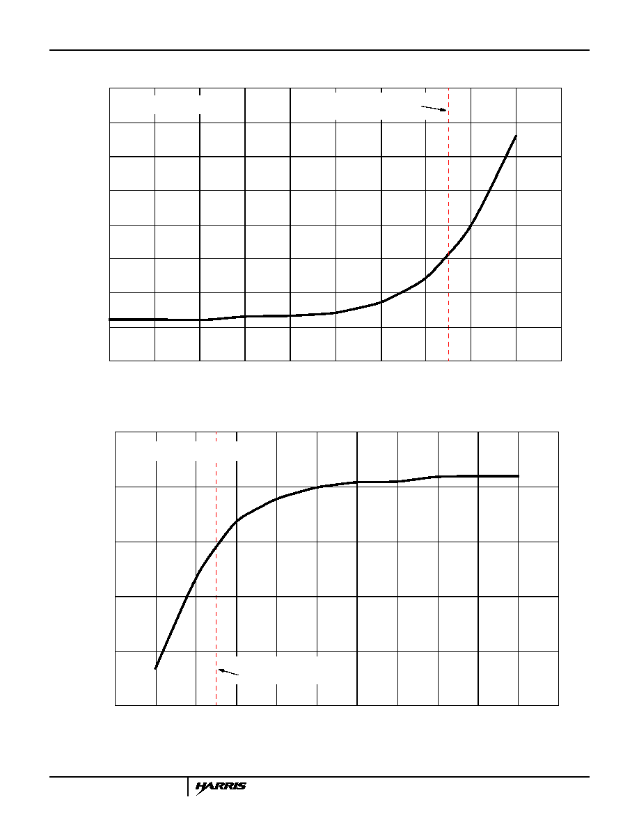
Typical Performance Curves
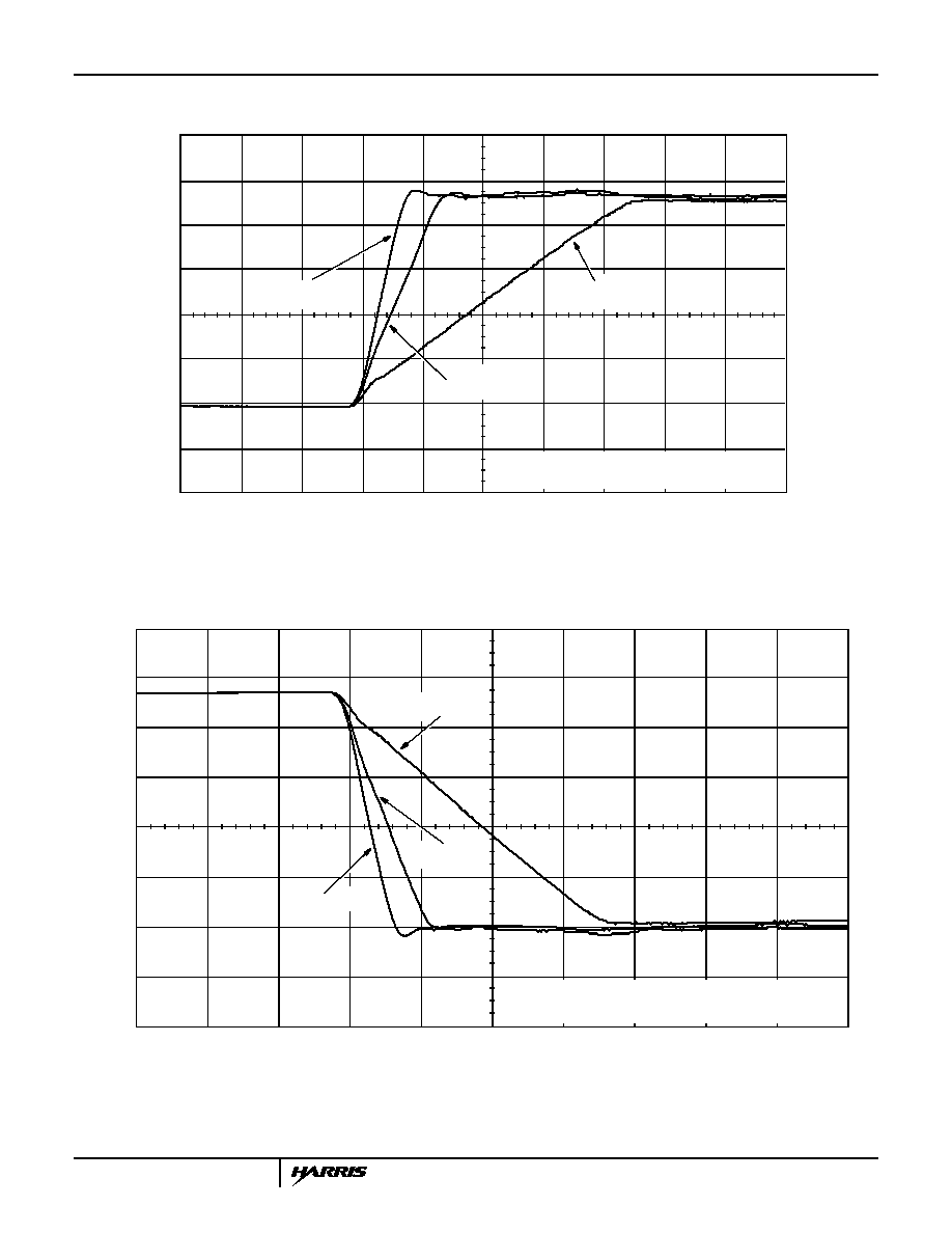
FIGURE 5. 5V STEP RESPONSE vs SLEW RATE CONTROL
FIGURE 6. 5V STEP RESPONSE vs SLEW RATE CONTROL
V
OUT
(V)
0
2
4
6
-2
TIME (ns)
0
4
8
10
12
20
2
6
14
16
18
I
STEAL
= 5mA
I
STEAL
= 0mA
I
STEAL
= 10mA
I
STEAL
= CURRENT FLOWING OUT OF +SRC FOR
RISING EDGE OR -SRC FOR FALLING EDGE
TIME (ns)
V
OU
T
(V
)
0
4
0
2
4
6
8
10
12
20
2
6
14
16
18
-2
I
STEAL
= CURRENT FLOWING OUT OF +SRC FOR
RISING EDGE OR -SRC FOR FALLING EDGE
I
STEAL
= -10mA
I
STEAL
= -5mA
I
STEAL
= 0mA
HFA5253
98
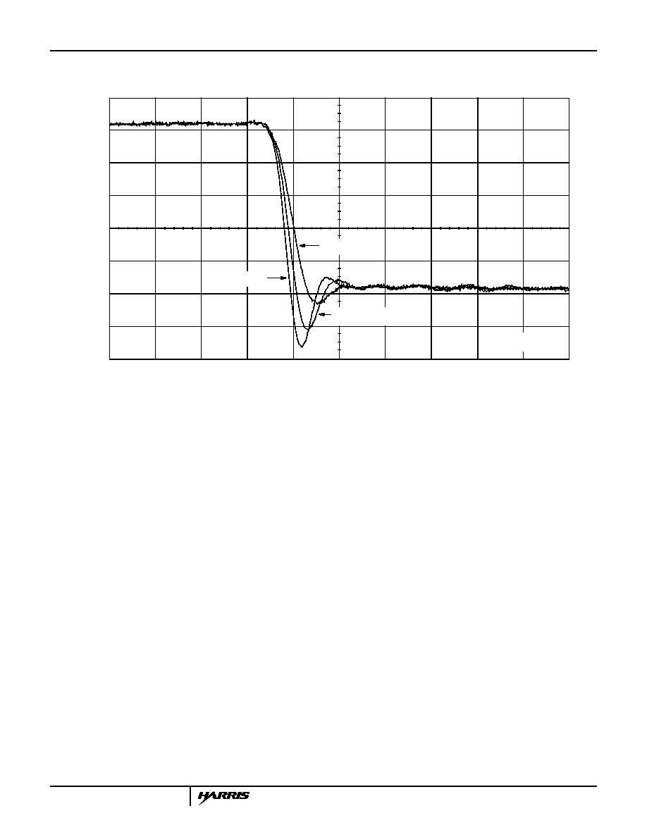
FIGURE 7. MINIMUM PULSE WIDTH, 1V/DIV.; 500ps/DIV.
FIGURE 8. V
OUT
ERROR vs V
IN
Typical Performance Curves
(Continued)
0
2.5
5
3
2
1
0
OU
TPU
T
(
V
)
1.087ns
TIME (ns)
-4
-2
0
2
4
6
8
10
-0.25
-0.2
-0.15
-0.1
-0.05
0
0.05
V
IN
(V)
V
OU
T
- V
IN
(V)
V
HIGH
V
LOW
HFA5253
99
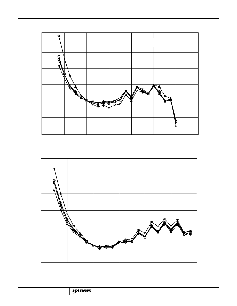
FIGURE 9. V
HIGH
LINEARITY ERROR 10.5V FULLSCALE
FIGURE 10. V
LOW
LINEARITY ERROR 10.5V FULLSCALE
Typical Performance Curves
(Continued)
-4
-2
0
2
4
6
8
10
-0.1
-0.05
0
0.05
0.1
0.15
0.2
V
IN
(V)
LI
NEARITY (%
O
F
10.5V FUL
L
SCA
L
E)
LI
NEA
R
ITY (V)
-0.01
-0.005
0.0
0.005
0.01
0.015
0.02
TYPICAL 5 UNITS
-4
-2
0
2
4
6
8
-0.05
0
0.05
0.1
0.15
0.2
0.25
V
IN
(V)
LINEARI
TY
(% OF 10
.
5
V FULLSCALE)
LINEARITY
(V
)
0.0
0.01
0.02
TYPICAL 5 UNITS
HFA5253
100
FIGURE 11. V
HIGH
/V
LOW
INTERACTION
FIGURE 12. V
HIGH
/V
LOW
INTERACTION
Typical Performance Curves
(Continued)
0
0.1
0.2
0.3
0.4
0.5
0.6
0.7
0.8
0.9
1
0.98
0.99
1
1.01
1.02
1.03
1.04
1.05
1.06
V
LOW
INPUT (V)
V
OUT
(V
)
MINIMUM RECOMMENDED
V
HIGH
TO V
LOW
VOLTAGE
V
HIGH
ACTIVE (NOMINAL 1.0V)
0
0.1
0.2
0.3
0.4
0.5
0.6
0.7
0.8
0.9
1
1.1
-0.04
-0.03
-0.02
-0.01
0
0.01
V
HIGH
INPUT (V)
V
OUT
(V)
MINIMUM RECOMMENDED
V
HIGH
TO V
LOW
VOLTAGE
V
LOW
ACTIVE (NOMINAL 0.0V)
HFA5253
101
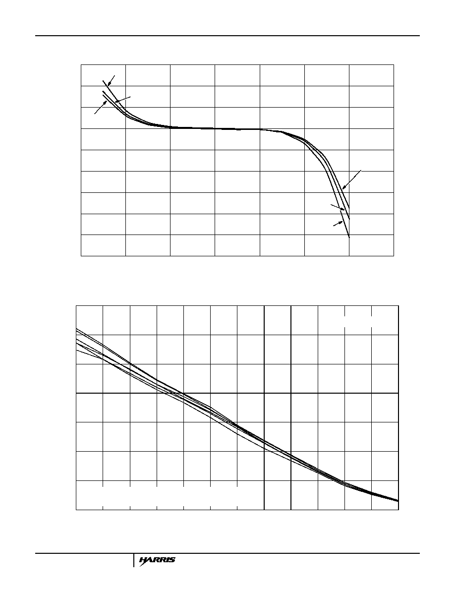
FIGURE 13. HIZ OUTPUT LEAKAGE
FIGURE 14. (+) SLEW RATE vs I
STEAL
Typical Performance Curves
(Continued)
-4
-2
0
2
4
6
8
10
-60
-50
-40
-30
-20
-10
0
10
20
30
OUTPUT VOLTAGE (V)
OUTPUT LEAKA
GE
(nA)
25
o
C
50
o
C
75
o
C
50
o
C
75
o
C
25
o
C
0
0.5
1
1.5
2
2.5
3
3.5
+SRC CURRENT (mA)
+SLEW R
A
TE (V/ns)
0
1
2
3
4
5
6
7
8
9
10
11
12
TYPICAL 6 UNITS
NOTE: SLEW RATE WILL CONTINUE TO DECLINE AS +SRC
CURRENT IS INCREASED BEYOND 12mA
HFA5253
102
FIGURE 15. (-) SLEW RATE vs I
STEAL
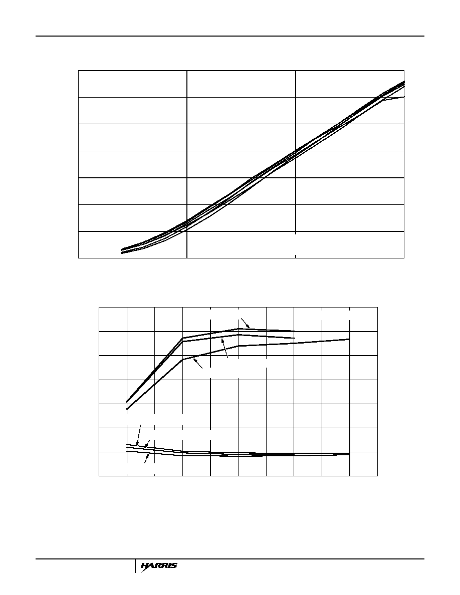
NOTE: The family of curves shows slew rate as a function of common mode voltage. A voltage is provided for each trace specifying one level of the
voltage step for which slew rate is measured. Example 1: Top Trace (V
HIGH
= 8V, I
STEAL
= 0mA). A voltage step of 1V goes from V
LOW
= 7V to
V
HIGH
= 8V and a voltage step of 9V goes from V
LOW
= -1V to V
HIGH
= 8V. Example 2: Trace (V
LOW
= -3V, I
STEAL
= 0mA). A voltage step of 1V
goes from V
LOW
= -3V to V
HIGH
= -2V and a voltage step of 9V goes from V
LOW
= -3V to V
HIGH
= 6V
.
FIGURE 16. (+) SLEW RATE vs AMPLITUDE
Typical Performance Curves
(Continued)
-15
-10
-5
0
0
0.5
1
1.5
2
2.5
3
3.5
-SRC CURRENT (mA)
-
SLE
W
R
A
TE
(
V
/ns
)
TYPICAL 6 UNITS
NOTE: SLEW RATE WILL CONTINUE TO DECLINE AS
-SRC CURRENT IS INCREASED BEYOND 12mA
0
1
2
3
4
5
6
7
8
9
10
0
0.5
1
1.5
2
2.5
3
3.5
VOLTAGE STEP (V
HIGH
- V
LOW
) (V)
+SLEW RA
TE (V/ns)
AVERAGE OF 8 UNITS
V
HIGH
= 8V, I
STEAL
= 10mA
V
HIGH
= 8V, I
STEAL
= 0mA
V
LOW
= 0V, I
STEAL
= 0mA
V
LOW
= -3V, I
STEAL
= 0mA
V
LOW
= -3V, I
STEAL
= 10mA
V
LOW
= 0V, I
STEAL
= 10mA
HFA5253

103
NOTE: The family of curves shows slew rate as a function of common mode voltage. A voltage is provided for each trace specifying one level of the
voltage step for which slew rate is measured. Example 1: Top Trace (V
HIGH
= 8V, I
STEAL
= 0mA). A voltage step of 1V goes from V
HIGH
= 8V to
V
LOW
= 7V and a voltage step of 9V goes from V
HIGH
= 8V to V
LOW
= -1V. Example 2: Trace (V
LOW
= -3V, I
STEAL
= 0mA). A voltage step of 1V
goes from V
HIGH
= -2V to V
LOW
= -3V and a voltage step of 9V goes from V
HIGH
= 6V to V
LOW
= -3V.
FIGURE 17. (-) SLEW RATE vs AMPLITUDE
FIGURE 18. 0.5V STEP RESPONSE vs C
LOAD
Typical Performance Curves
(Continued)
0
1
2
3
4
5
6
7
8
9
10
0.5
1
1.5
2
2.5
3
3.5
4
VOLTAGE STEP (V
HIGH
-V
LOW
) (V)
-SL
E
W RA
TE
(
V
/n
s
)
V
LOW
= 0V, I
STEAL
= 0mA
AVERAGE OF 8 UNITS
V
HIGH
= 8V, I
STEAL
= 10mA
V
LOW
= 0V, I
STEAL
= 10mA
V
LOW
= -3V, I
STEAL
= 10mA
V
HIGH
= 8V, I
STEAL
= 0mA
V
LOW
= -3V, I
STEAL
= 0mA
TIME (ns)
0
2
4
5
6
10
1
3
7
8
9
V
OU
T
(V
)
0
0.2
0.4
0.6
Z
LOAD
= 1k
|| C
LOAD
C
LOAD
= 10.2pF
C
LOAD
= 4pF
C
LOAD
= 6.5pF
HFA5253
104
FIGURE 19. 0.5V STEP RESPONSE vs C
LOAD
Typical Performance Curves
(Continued)
TIME (ns)
0
2
4
5
6
10
1
3
7
8
9
V
OUT
(V)
0
0.2
0.4
0.6
-0.2
Z
LOAD
= 1k
|| C
LOAD
C
LOAD
= 10.2pF
C
LOAD
= 4pF
C
LOAD
= 6.5pF
HFA5253
105
Die Characteristics
DIE DIMENSIONS:
2670
µ
m x 1730
µ
m x 525
µ
m
METALLIZATION:
Type: Metal 1: Cu (2%) SiAl/TiW
Thickness: Metal 1: 8k
≈
±
0.4k
≈
Backside: Gold
Type: Metal 2: Cu (2%) Al
Thickness: Metal 2: 16k
≈
±
0.8k
≈
PASSIVATION:
Nitride, 4k
≈
±
0.5k
≈
TRANSISTOR COUNT:
113
SUBSTRATE POTENTIAL:
Floating
Metallization Mask Layout
HFA5253
DATA
DATA
HIZ
HIZ
V
HIGH
V
LOW
V
EE1
V
CC1
V
OUT
V
CC2
V
EE2
+SRC
-SRC
HFA5253

106
HFA5253
Power Small Outline Plastic Packages (PSOP)
INDEX
AREA
E
D
N
1
2
3
-B-
0.25(0.010)
C A
M
B S
e
-A-
L
B
M
-C-
A1
A
SEATING PLANE
0.10(0.004)
h x 45
o
C
H
µ
0.25(0.010)
B
M
M
N
1
2
3
D1
E1
POWER SOP PACKAGE
(HEAT SLUG SURFACE IS ELECTRICALLY FLOATING)
TOP VIEW
M20.3A
20 LEAD POWER SMALL OUTLINE PLASTIC PACKAGE
SYMBOL
INCHES
MILLIMETERS
NOTES
MIN
MAX
MIN
MAX
A
0.0926
0.1043
2.35
2.65
-
A1
0.0040
0.0118
0.10
0.30
-
B
0.013
0.0200
0.33
0.51
9
C
0.0091
0.0125
0.23
0.32
-
D
0.4961
0.5118
12.60
13.00
3
D1
0.325
0.340
8.25
8.63
10
E
0.2914
0.2992
7.40
7.60
4
E1
0.175
0.190
4.44
4.82
10
e
0.050 BSC
1.27 BSC
-
H
0.394
0.419
10.00
10.65
-
h
0.010
0.029
0.25
0.75
5
L
0.016
0.050
0.40
1.27
6
N
20
20
7
0
o
8
o
0
o
8
o
-
Rev. 0 6/95
NOTES:
1. Symbols are defined in the "MO Series Symbol List" in Section
2.2 of Publication Number 95.
2. Dimensioning and tolerancing per ANSI Y14.5M-1982.
3. Dimension "D" does not include mold flash, protrusions or
gate burrs. Mold flash, protrusion and gate burrs shall not ex-
ceed 0.15mm (0.006 inch) per side.
4. Dimension "E" does not include interlead flash or protrusions.
Interlead flash and protrusions shall not exceed 0.25mm
(0.010 inch) per side.
5. The chamfer on the body is optional. If it is not present, a vi-
sual index feature must be located within the crosshatched
area.
6. "L" is the length of terminal for soldering to a substrate.
7. "N" is the number of terminal positions.
8. Terminal numbers are shown for reference only.
9. The lead width "B", as measured 0.36mm (0.014 inch) or
greater above the seating plane, shall not exceed a maxi-
mum value of 0.61mm (0.024 inch)
10. Exposed copper heat slug flush with top surface of package.
All other dimensions conform to JEDEC MS-013AC Issue C.
11. Controlling dimension: MILLIMETER. Converted inch di-
mensions are not necessarily exact.