LED SPECIFICATION
Page: 1
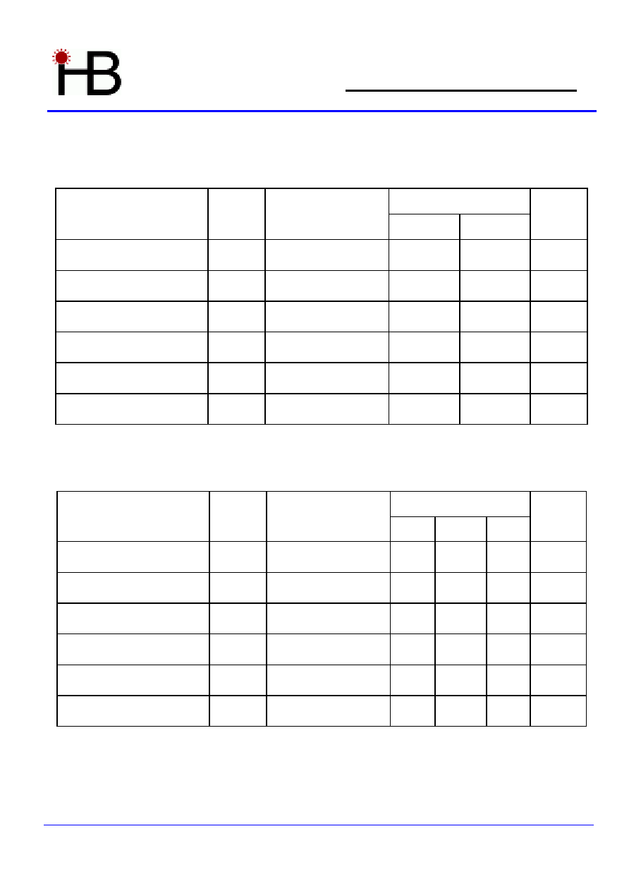
Features
Single color
High bright output
Low power consumption
High reliability and long life
Descriptions
Dice material
Emitting Color
Super Bright Blue
Device Outline
10mm Round Type
Lens Type
Blue diffused
Directivity
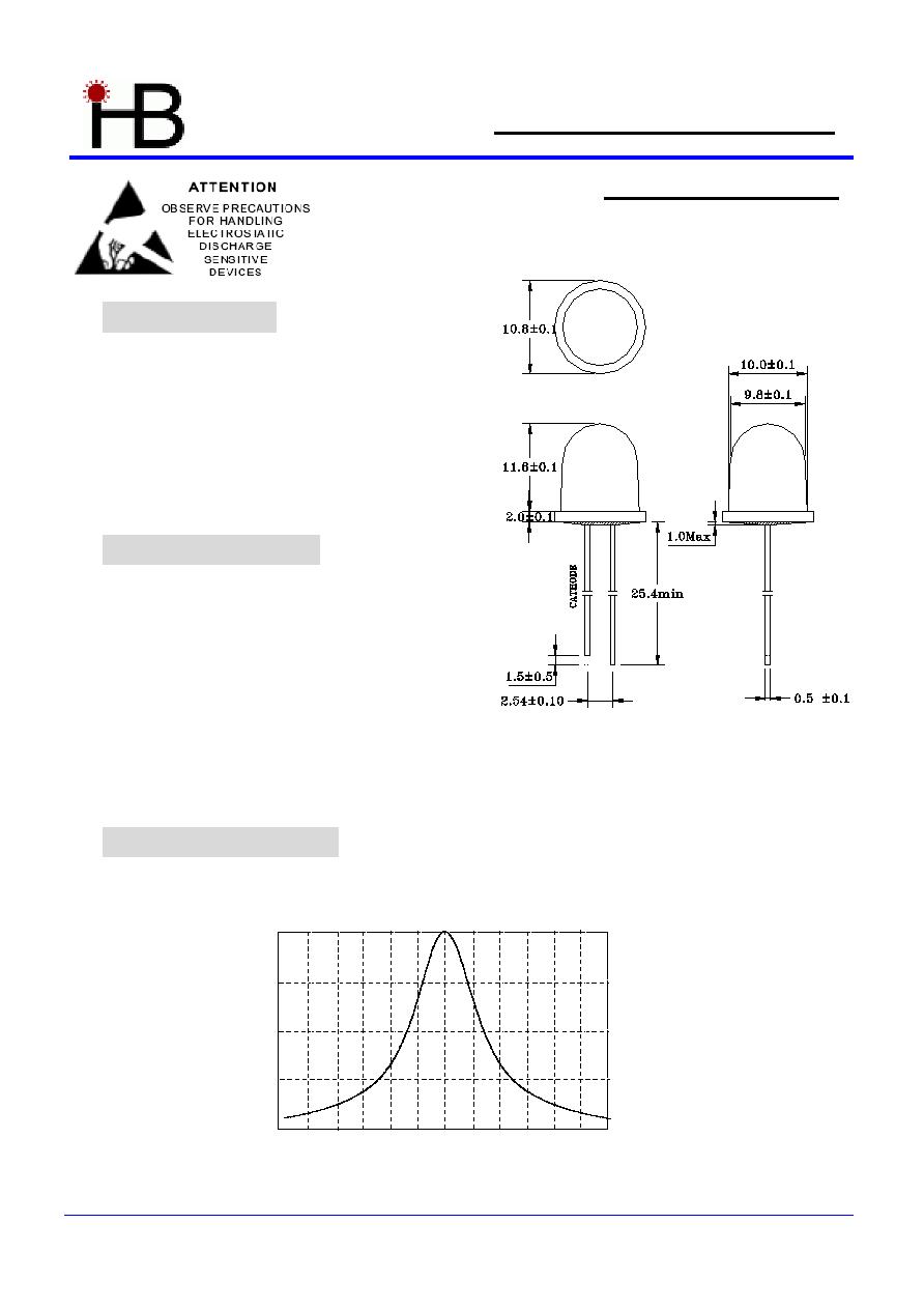
1. All dimensions are millimeters
2. Tolerance is +/-0.25mm unless otherwise noted
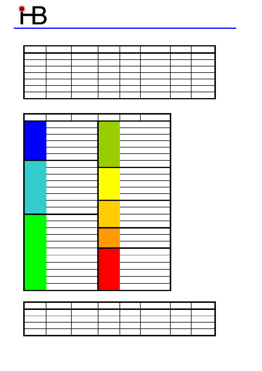
105LB7D
-90
-75
-60
-45
-30
-15
0
15
30
45
60
75
90
LED SPECIFICATION
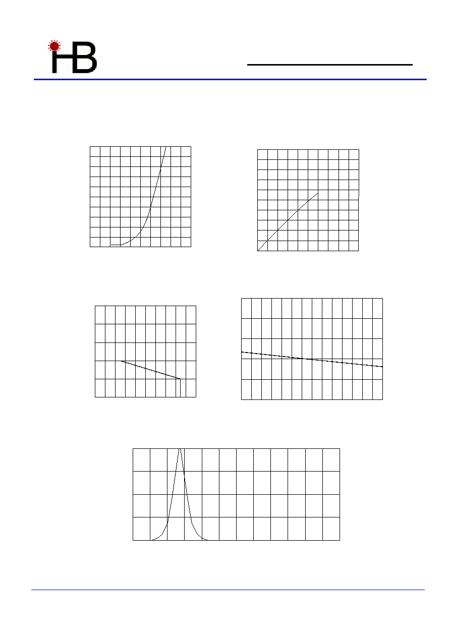
Typical electrical/optical characteristic curves
50
40
30
4.0
0
0
50
FORWARD CURRENT Vs
FORWARD VOLTAGE
LUMINOUS INTENSITY Vs.
FORWARD CURRENT
40
50
2.0
1.5
40
30
0.5
20
10
3.6
0
10
2.4
2.0
2.8
0
3.2
20
Forwar
d Current(
m
A)
Lu
m
i
no
u
s
I
n
tensity
Re
lati
ve Va
lue a
t
IF=
2
0
m
A
1.0
30
2.5
FORWARD CURRENT
DERATING CURVE
2.0
1.5
20
2.5
LUMINOUS INTENSITY Vs.
AMBIENT TEMPERATURE
100
80
60
0.5
20
0
-20
100
-40
60
80
20
40
0
0
Ambient Temperature T
A
( )
Ambient Temperature T
A
( )
40
R
e
l
a
t
i
ve
Lu
m
i
no
us
Intensity
Forward Current(
m
A)
10
1.0
IF-Forward Current (mA)
Forward Voltage(V)
700
650
400
100
R
e
lativ
e
L
u
minou
s
Intensity
Wavelength
(nm)
0
50
25
75
550
600
500
450
Page:
4

LED LAMP
APPLICATION
SOLDERING
METHOD SOLDERING
CONDITIONS
REMARK
DIP
SOLDERING
Bath temperature: 260±5
Immersion time: with 5 sec
Solder no closer than 3mm from the
base of the package
Using soldering flux," RESIN FLUX"
is recommended.
SOLDERING
IRON
Soldering iron: 30W or smaller
Temperature at tip of iron: 260 or lower
Soldering time: within 5 sec.
During soldering, take care not to
press the tip of iron against the
lead.
(To prevent heat from being
transferred directly to the lead, hold
the lead with a pair of tweezers
while soldering
1) When soldering the lead of LED in a condition that the package is fixed with a panel (See Fig.1),
be careful not to stress the leads with iron tip.
2) When soldering wire to the lead, work with a Fig (See Fig.2) to avoid stressing the package.
Page : 5
P a n e l
(Fig.1)
L e a d w r i e s
L e a v e a s l i g h t
c l e a r a n c e
L e a d w r i e s
( F i g . 2 )