 | –≠–ª–µ–∫—Ç—Ä–æ–Ω–Ω—ã–π –∫–æ–º–ø–æ–Ω–µ–Ω—Ç: 2SC1472K | –°–∫–∞—á–∞—Ç—å:  PDF PDF  ZIP ZIP |

2SC1472(K)
Silicon NPN Epitaxial, Darlington
Application
High gain amplifier
Outline
1. Emitter
2. Collector
3. Base
3
2
1
TO-92 (1)
3
2
1

2SC1472 (K)
2
Absolute Maximum Ratings (Ta = 25∞C)
Item
Symbol
Ratings
Unit
Collector to base voltage
V
CBO
40
V
Collector to emitter voltage
V
CEO
30
V
Emitter to base voltage
V
EBO
10
V
Collector current
I
C
300
mA
Collector peak current
i
C(peak)
500
mA
Collector power dissipation
P
C
500
mW
Junction temperature
Tj
150
∞
C
Storage temperature
Tstg
≠55 to +150
∞
C

2SC1472 (K)
3
Electrical Characteristics (Ta = 25∞C)
Item
Symbol
Min
Typ
Max
Unit
Test conditions
Collector to emitter breakdown
voltage
V
(BR)CEO
30
--
--
V
I
C
= 1 mA, R
BE
=
Collector cutoff current
I
CBO
--
--
100
nA
V
CB
= 30 V, I
E
= 0
Emitter cutoff current
I
EBO
--
--
100
nA
V
EB
= 10 V, I
C
= 0
DC current transfer ratio
h
FE1
*
1
2000
--
100000
I
C
= 10 mA, V
CE
= 5 V
h
FE2
*
1
3000
--
--
I
C
= 100 mA, V
CE
= 5 V
(Pulse Test)
h
FE3
*
1
3000
--
--
I
C
= 400 mA, V
CE
= 5 V
(Pulse Test)
Collector to emitter saturation
voltage
V
CE(sat)
--
--
1.5
V
I
C
= 100 mA, I
B
= 0.1 mA
Base to emitter voltage
V
BE(sat)
--
--
2.0
V
I
C
= 100 mA, I
B
= 0.1 mA
Gain bandwidth product
f
T
50
--
--
MHz
V
CE
= 5 V, I
C
= 10 mA
Collector output capacitance
Cob
--
--
10
pF
V
CB
= 10 V, I
E
= 0, f = 1 MHz
Turn on time
t
on
--
60
--
ns
V
CC
= 11 V
I
C
= 100 I
B1
= 100 mA
I
B2
= ≠I
B1
Turn off time
t
off
--
800
--
ns
Storage time
t
stg
--
350
--
ns
Note:
1. The 2SC1472(K) is grouped by h
FE
as follows.
A
B
h
FE1
2000 to 100000 5000 to 100000
h
FE2
3000 min
10000 min
h
FE3
3000 min
10000 min
Switching Time Test Circuit
50
50
0.002
≠6 V
6 k
100
11 V
6 k
D.U.T.
CRT
P.G.
tr, tf
15 ns
PW
10
µ
s
duty ratio
10%
+
≠
50
0.002
+
≠
Unit R :
C :
µ
F
13 V
0
0
10%
Response Waveform
90%
t
on
t
off
t
d
t
stg
Input
Output
90%
10%
10%
90%

2SC1472 (K)
4
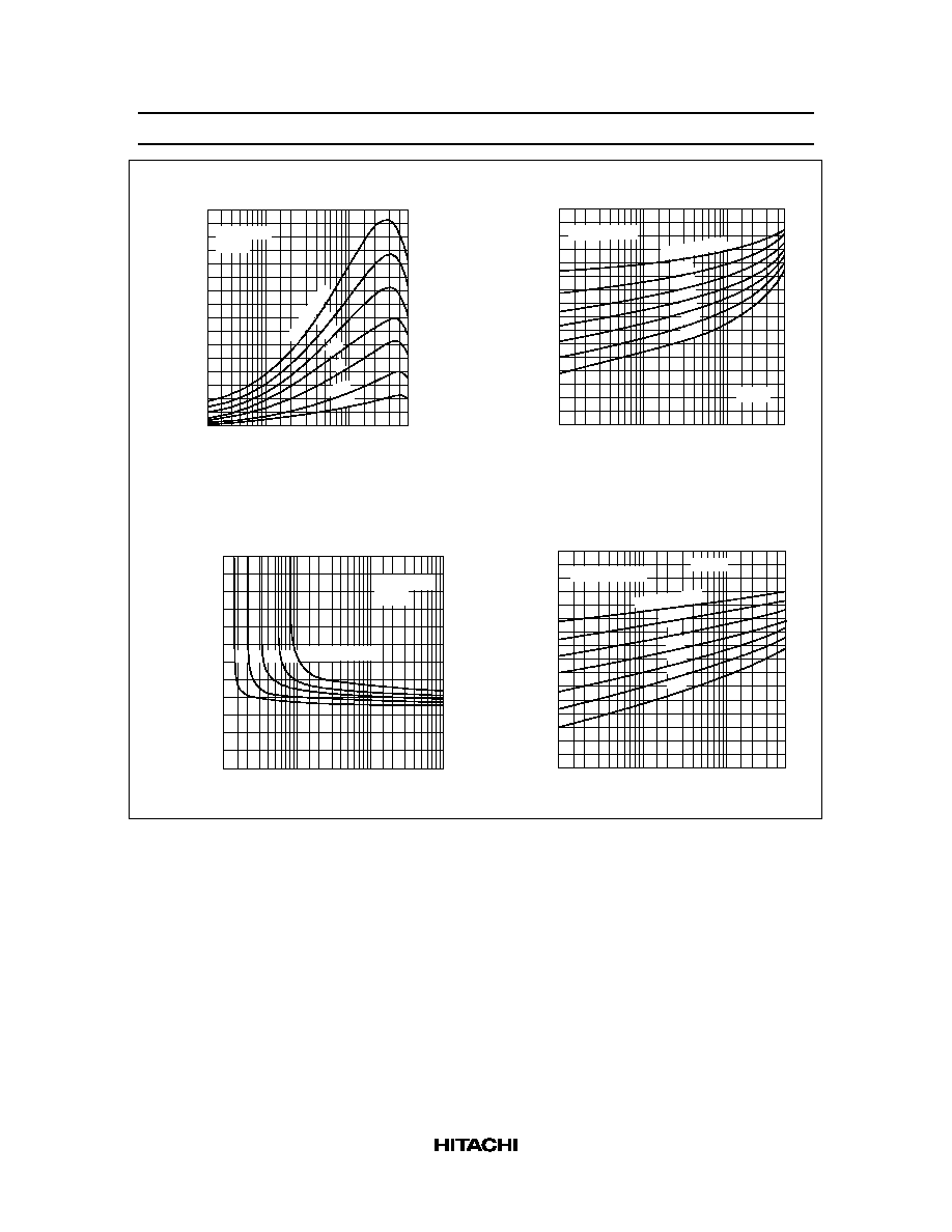
150
50
100
Ambient Temperature Ta (
∞
C)
600
400
200
0
Maximum Collector Dissipation Curve
Collector Power Dissipation P
C
(mW)
10
2.0
6.0
4.0
8.0
Collector to Emitter Voltage V
CE
(V)
500
300
400
200
100
0
Typical Output Characteristics
Collector Current I
C
(mA)
I
B
= 0
2
µ
A
4
6
8
10
12
20
25
14
16
18
30
35
P
C
= 500 mW
50
10
30
20
40
Collector to Emitter Voltage V
CE
(V)
200
120
160
80
40
0
Typical Output Characteristics
Collector Current I
C
(mA)
I
B
= 0
0.5
µ
A
Pulse
1.0
1.5
2.0
2.5
3.0
3.5
4.0
4.5
5.0
P
C
= 500 mW
Collector to Emitter Voltage V
CE
(V)
10,000
1,000
100
10
1.0
0.1
0.01
0
10
30
20
Collector Cutoff Current vs.
Collector to Emitter Voltage
Collector Cutoff Current I
CEO
(nA)
T
C
= 25
∞
C
R
BE
=
50
75
100
2SC1472 (K)
5
500
100
5.0
50
20
10
200
Collector Current I
C
(mA)
80
50
40
30
20
10
0
70
60
2.0
DC Current Transfer Ratio vs.
Collector Current
DC Current Transfer Ratio h
FE
(
◊
10
3
)
V
CE
= 5 V
Pulse
Ta = 100
∞
C
75
50
25
≠25
≠50
0
500
100
5
50
20
10
200
Collector Current I
C
(mA)
1.1
1.0
0.9
0.8
0.7
0.6
0.5
0.4
0.3
1
2
Collector to Emitter Saturation
Voltage vs. Collector Current
Collector to Emitter Saturation Voltage
V
CE (sat)
(V)
I
C
= 1,000 I
B
Ta = ≠50
∞
C
Pulse
≠25
25
50
75
100
0
Base Current I
B
(
µ
A)
2.4
2.0
1.6
1.2
0.8
0.4
0
1
100
30
300
3
10
1,000
Collector to Emitter Saturation
Voltage vs. Base Current
Collector to Emitter Saturation Voltage
V
CE (sat)
(V)
Pulse
Ta = 25
∞
C
I
C
= 500 mA
20 50 100 200
75
Collector Current I
C
(mA)
2.0
1.8
1.6
1.4
1.2
1.0
0.8
0.6
0.4
1
100
20
200
2
10
5
50
500
Base to Emitter Saturation
Voltage vs. Collector Current
Base to Emitter Saturation Voltage
V
BE (sat)
(V)
Pulse
I
C
= 1,000 I
B
Ta = ≠50
∞
C
≠25
25
50
100
0