 | –≠–ª–µ–∫—Ç—Ä–æ–Ω–Ω—ã–π –∫–æ–º–ø–æ–Ω–µ–Ω—Ç: 2SC2898 | –°–∫–∞—á–∞—Ç—å:  PDF PDF  ZIP ZIP |

2SC2898
Silicon NPN Triple Diffused
Application
High voltage, high speed and high power switching
Outline
1. Base
2. Collector
(Flange)
3. Emitter
TO-220AB
1
2
3
Absolute Maximum Ratings (Ta = 25∞C)
Item
Symbol
Ratings
Unit
Collector to base voltage
V
CBO
500
V
Collector to emitter voltage
V
CEO
400
V
Emitter to base voltage
V
EBO
7
V
Collector current
I
C
8
A
Collector peak current
I
C(peak)
16
A
Base current
I
B
4
A
Collector power dissipation
P
C
*
1
50
W
Junction temperature
Tj
150
∞
C
Storage temperature
Tstg
≠55 to +150
∞
C
Note:
1. Value at T
C
= 25
∞
C.

2SC2898
2
Electrical Characteristics (Ta = 25∞C)
Item
Symbol
Min
Typ
Max
Unit
Test conditions
Collector to emitter sustain
voltage
V
CEO(sus)
400
--
--
V
I
C
= 0.2 A, R
BE
=
,
L = 100 mH
Collector to emitter sustain
voltage
V
CEX(sus)
400
--
--
V
I
C
= 8 A, I
B1
= 1.6 A,
I
B2
= ≠0.8 A, V
BE
= ≠5 V,
L = 180
µ
H, Clamped
Emitter to base breakdown
voltage
V
(BR)EBO
7
--
--
V
I
E
= 10 mA, I
C
= 0
Collector cutoff current
I
CBO
--
--
50
µ
A
V
CB
= 400 V, I
E
= 0
I
CEO
--
--
50
µ
A
V
CE
= 350 V, R
BE
=
DC current transfer ratio
h
FE1
15
--
--
V
CE
= 5 V, I
C
= 4 A*
1
h
FE2
7
--
--
V
CE
= 5 V, I
C
= 8 A*
1
Collector to emitter saturation
voltage
V
CE(sat)
--
--
1.0
V
I
C
= 4 A, I
B
= 0.8 A*
1
Base to emitter saturation
voltage
V
BE(sat)
--
--
1.5
V
Turn on time
t
on
--
--
0.8
µ
s
I
C
= 8 A, I
B1
= ≠I
B2
= 1.6 A,
Storage time
t
stg
--
--
2.0
µ
s
V
CC
150 V
Fall time
t
f
--
--
0.8
µ
s
Note:
1. Pulse test
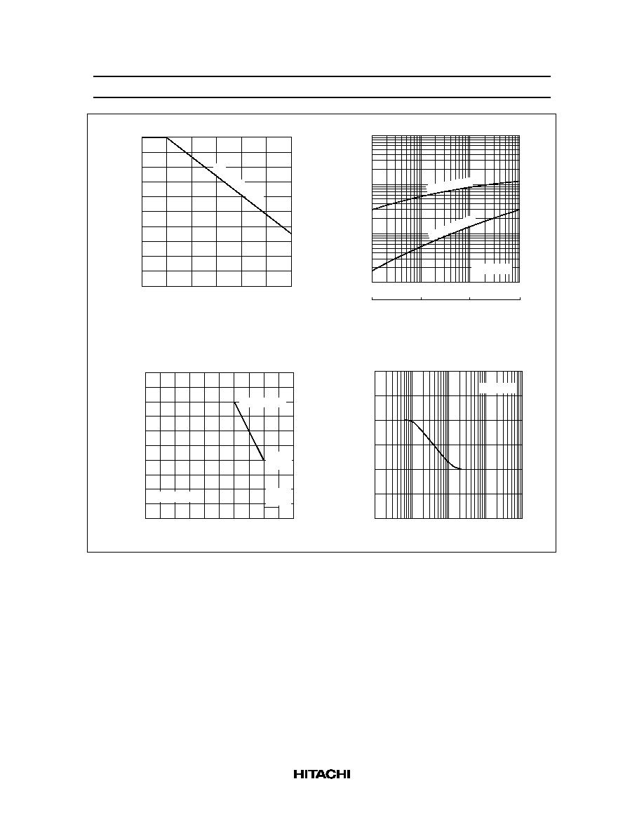
60
40
20
0
50
100
150
Case temperature T
C
(
∞
C)
Collector power dissipation P
C
(W)
Maximum Collector Dissipation Curve
10
0.01
300
1,000
Collector to emitter voltage V
CE
(V)
Collector current I
C
(A)
Area of Safe Operation
100
1.0
0.1
1
3
30
10
100
I
C(max)
(Continuous)
I
C(peak)
Ta = 25
∞
C, 1 Shot
25
µ
s
50
µ
s
250
µ
s
1 ms
DC Operation (T
C
= 25
∞
C)
PW = 10 ms
2SC2898
3
100
80
60
40
20
0
50
100
150
Case temperature T
C
(
∞
C)
Collector current derating rate (%)
Collector Current Derating Rate
IS/B Limit Area
10
3
10 (s)
Transient Thermal Resistance
1.0
0.03
0.01
0.1
1.0
0.01
10 (ms)
0.1
1.0
0.01
0.1
0.3
Thermal resistence
j-c
(
∞
C/W)
10 ms≠10 s
10
µ
s≠10 ms
T
C
= 25
∞
C
20
200
500
Collector to emitter voltage V
CE
(V)
Reverse Bias Area of Safe Operation
16
4
100
300
400
0
8
12
I
B2
= ≠0.8 A
450 V,
1.5 A
300 V, 16 A
400 V,
8 A
Collector current I
C
(A)
600
Base to emitter resistance R
BE
(
)
Collector to Emitter Voltage vs.
Base to Emitter Resistance
400
300
1 k
10 k
100 k
1 M
100
500
I
C
= 1 mA
Collector to emitter voltage V
(BR)CER
(V)
2SC2898
4
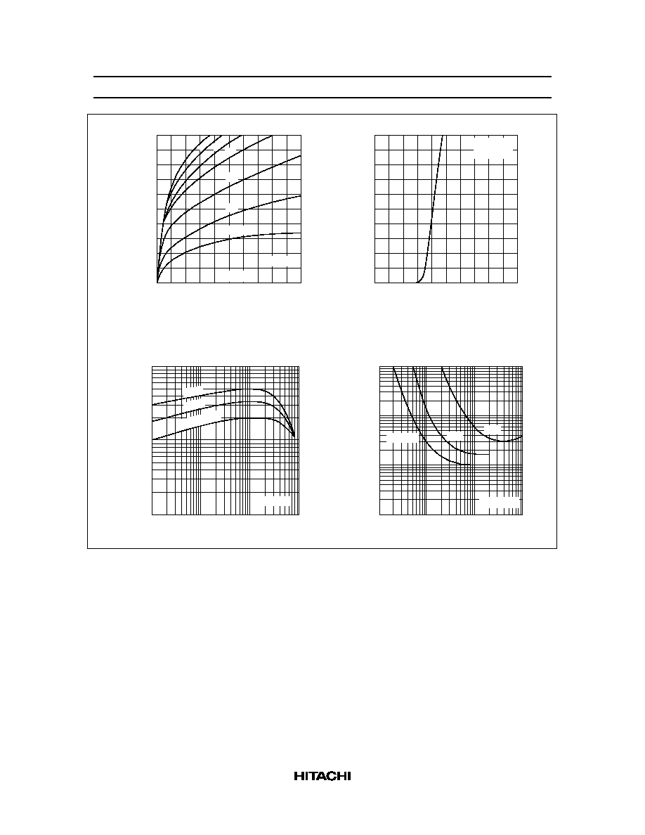
5
2
5
Collector to emitter voltage V
CE
(V)
Typical Output Characteristics
4
1
1
3
4
0
2
3
I
B
= 0
T
C
= 25
∞
C
0.05 A
0.1
0.2
0.3
0.4
0.5
0.6
Collector current I
C
(A)
5
0.8
2.0
Base to emitter voltage V
BE
(V)
Typical Transfer Characteristics
4
1
0.4
1.2
1.6
0
2
3
T
C
= 25
∞
C
V
CE
= 5 V
Collector current I
C
(A)
100
3
Collector current I
C
(A)
DC current transfer ratio h
FE
30
0.03
0.1
1.0
10
1
10
DC Current Transfer Ratio vs.
Collector Current
T
C
= ≠25
∞
C
V
CE
= 5 V
0.01
3
0.3
75
∞
C
25
∞
C
10
Base current I
B
(A)
Collector to emitter saturation voltage V
CE(sat)
(V)
3
0.1
0.03
0.1
0.3
10
0.01
0.3
1.0
Collector to Emitter Saturation
Voltage vs. Base Current
I
C
= 1 A
T
C
= 25
∞
C
0.01
0.03
1.0
3
2 A
5 A
2SC2898
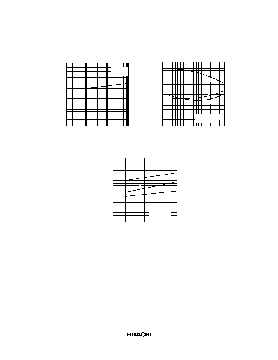
5
10
10
Collector current I
C
(A)
Base to emitter saturation voltage V
BE(sat)
(V)
1.0
3
0.03
0.03
0.1
1.0
3
0.01
0.1
0.3
Base to Emitter Saturation Voltage
vs. Collector Current
T
C
= 25
∞
C
I
C
= 5 I
B
0.01
0.3
I
C
= 5 I
B1
= ≠5 I
B2
V
CC
= 150 V
t
stg
t
f
t
on
10
0.1
10
3
Collector current I
C
(A)
Switching time t (
µ
s)
Switching Time vs. Collector Current
0.03
0.1
0.03
0.01
0.3
1.0
0.01
0.3
1.0
3
.
.
I
C
= 8 A
I
B1
= I
B2
= 1.6 A
R
L
= 19
V
CC
= 150 V
t
stg
t
f
t
on
5
50
125
Case temperature T
C
(
∞
C)
Switching time t (
µ
s)
Switching Time vs. Case Temperature
0.05
0.3
0.1
25
0
75
100
1.0
3
.
.