 | –≠–ª–µ–∫—Ç—Ä–æ–Ω–Ω—ã–π –∫–æ–º–ø–æ–Ω–µ–Ω—Ç: 2SC3510 | –°–∫–∞—á–∞—Ç—å:  PDF PDF  ZIP ZIP |
2SC3127, 2SC3128, 2SC3510
Silicon NPN Epitaxial
Application
UHF/VHF wide band amplifier
Outline
1
2
3
1. Emitter
2. Base
3. Collector
MPAK
2SC3127
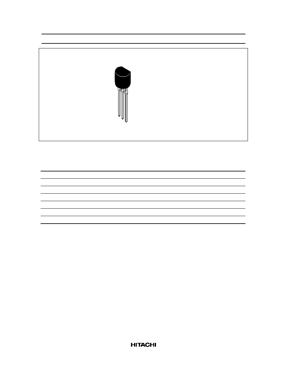
2SC3127, 2SC3128, 2SC3510
2
1. Base
2. Emitter
3. Collector
TO-92 (2)
2SC3128, 2SC3510
3
2
1
Absolute Maximum Ratings (Ta = 25∞C)
Item
Symbol
2SC3127*
1
2SC3128
2SC3510
Unit
Collector to base voltage
V
CBO
20
20
20
V
Collector to emitter voltage
V
CEO
12
12
12
V
Emitter to base voltage
V
EBO
3
3
3
V
Collector current
I
C
50
50
50
mA
Collector power dissipation
P
C
150
350
600
mW
Junction temperature
Tj
150
150
150
∞
C
Storage temperature
Tstg
≠55 to +150
≠55 to +150
≠55 to +150
∞
C
Note:
1. Marking for 2SC3127 is "ID≠".
2SC3127, 2SC3128, 2SC3510
3
Electrical Characteristics (Ta = 25∞C)
Item
Symbol
Min
Typ
Max
Unit
Test conditions
Collector to base breakdown
voltage
V
(BR)CBO
20
--
--
V
I
C
= 10
µ
A, I
E
= 0
Collector to emitter breakdown
voltage
V
(BR)CEO
12
--
--
V
I
C
= 1 mA, R
BE
=
Emitter cutoff current
I
EBO
--
--
10
µ
A
V
EB
= 3 V, I
C
= 0
Collector cutoff current
I
CBO
--
--
0.5
µ
A
V
CB
= 12 V, I
E
= 0
DC current transfer ratio
h
FE
30
90
200
V
CE
= 5 V, I
C
= 20 mA
Collector output capacitance
Cob
--
0.9
1.5
pF
V
CB
= 5 V, I
E
= 0, f = 1 MHz
Gain bandwidth product
f
T
3.5
4.5
--
GHz
V
CE
= 5 V, I
C
= 20 mA
Power gain
PG
--
10.5
--
dB
V
CE
= 5 V, I
C
= 20 mA,
f = 900 MHz
Noise figure
NF
--
2.2
--
dB
V
CE
= 5 V, I
C
= 5 mA,
f = 900 MHz
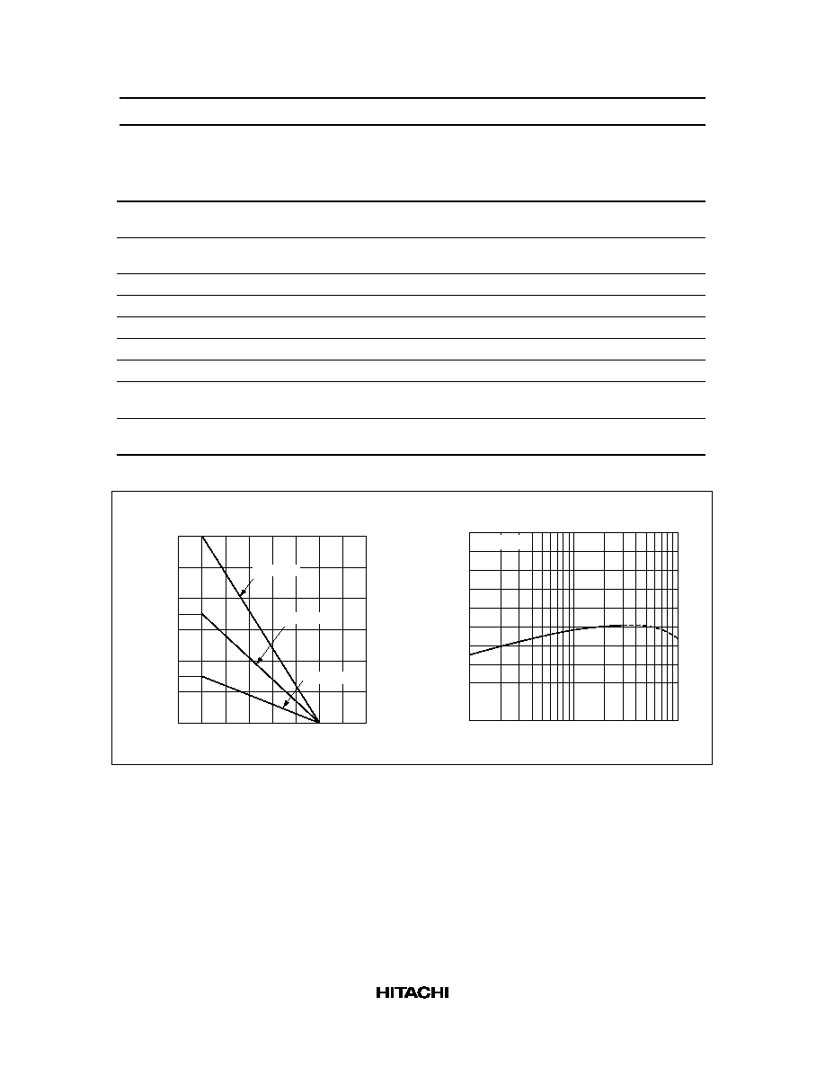
Maximum Collector Dissipation Curve
600
400
200
0
50
100
150
200
Ambient Temperature Ta (
∞
C)
Collector Power Dissipation Pc (mW)
2SC3510
2SC3128
2SC3127
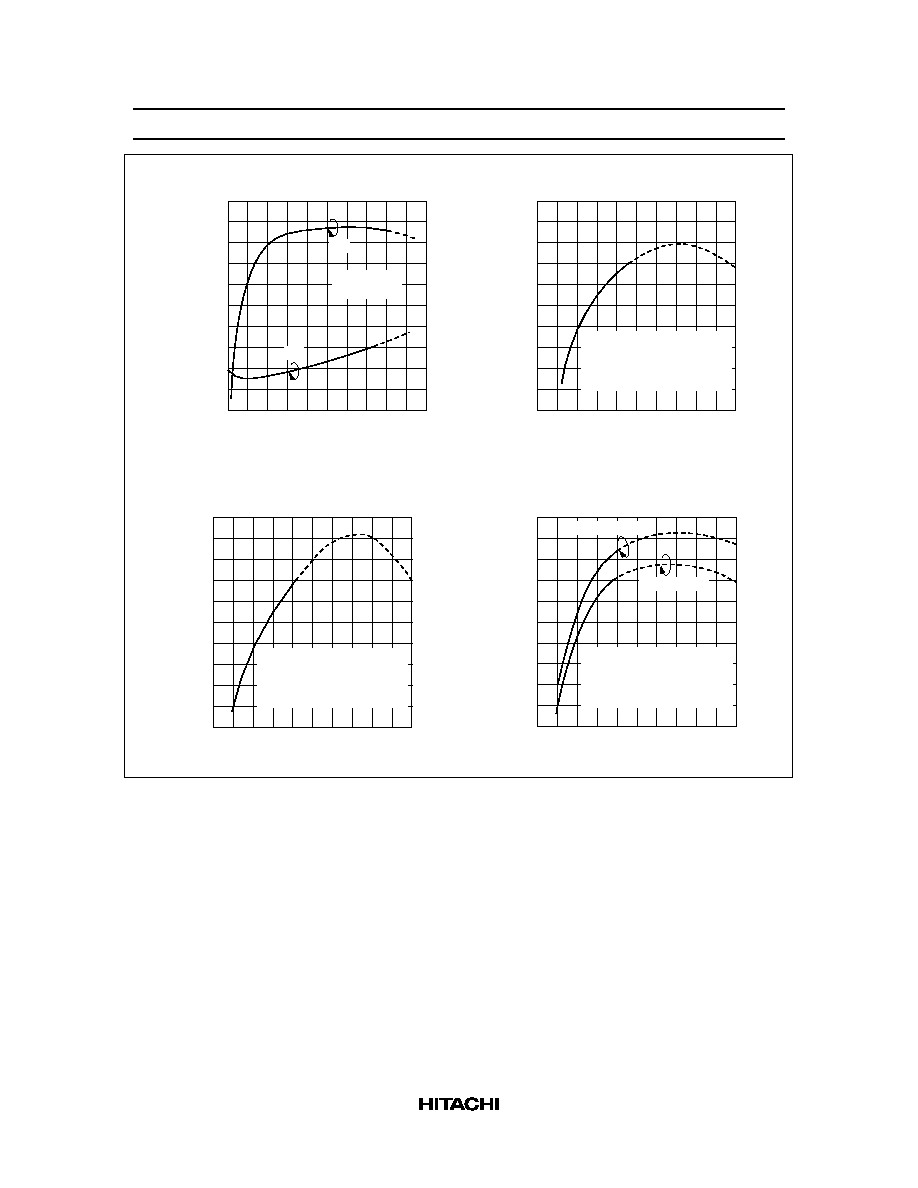
DC Current Transfer Ratio vs.
Collector Current
Collector Current I
C
(mA)
1
2
5
10
20
50
100
0
40
80
120
160
200
DC Current Transfer Ratio h
FE
V
CE
= 5 V
2SC3127, 2SC3128, 2SC3510
4
Gain Bandwidth Product vs.
Collector Current
0
1.0
2.0
3.0
4.0
5.0
Collector Current I
C
(mA)
Gain Bandwidth Product f
T
(GHz)
1
2
5
10
20
50
V
CE
= 5 V
f = 500 MHz
Collector Output Capacitance vs.
Collector to Base Voltage
Collector Output Capacitance C
ob
(pF)
Collector to Base Voltage V
CB
(V)
0
0.4
0.8
1.2
1.6
2.0
1
2
5
10
20
50
f = 1 MHz
I
E
= 0
Reverse Transfer Capacitance C
re
(pF)
Collector to Base Voltage V
CB
(V)
0
0.4
0.8
1.2
1.6
2.0
1
2
5
10
20
50
Reverse Transfer Capacitance vs.
Collector to Base Voltage
f = 1 MHz
Emitter Common
Power Gain and Noise Figure vs.
Collector Current
Power Gain PG (dB)
Noise Figure NF (dB)
Collector Current I
C
(mA)
0
4
8
12
16
20
0
10
20
30
40
50
V
CE
= 5 V
f = 500 MHz
PG
NF
2SC3127, 2SC3128, 2SC3510
5
Power Gain and Noise Figure vs.
Collector Current
Power Gain PG (dB)
Noise Figure NF (dB)
Collector Current I
C
(mA)
2
4
6
8
10
12
0
10
20
30
40
50
V
CE
= 5 V
f = 900 MHz
PG
NF
2nd I.M. Distortion 2nd I.M.D. (dB)
Collector Current I
C
(mA)
20
30
40
50
60
70
0
10
20
30
40
50
2nd I.M. Distortion vs. Collector Current
V
CC
= 12 V
f
1
= 210 MHz, f
2
= 200 MHz
V
out
= 100 dB
µ
f
2nd
= 410 MHz
2nd I.M. Distortion 2nd I.M.D. (dB)
Collector Current I
C
(mA)
20
30
40
50
60
70
0
10
20
30
40
50
2nd I.M. Distortion vs. Collector Current
V
CC
= 12 V
f
1
= 600 MHz, f
2
= 650 MHz
V
out
= 100 dB
µ
f
2nd
= 1,250 MHz
3rd I.M. Distortion 3rd I.M.D. (dB)
Collector Current I
C
(mA)
30
40
50
60
70
80
0
10
20
30
40
50
3rd I.M. Distortion vs. Collector Current
V
CC
= 12 V
f
1
= 210 MHz, f
2
= 200 MHz
V
out
= 100 dB
µ
f
3rd
= 190 MHz, 220 MHz
f = 190 MHz
f = 220 MHz