 | –≠–ª–µ–∫—Ç—Ä–æ–Ω–Ω—ã–π –∫–æ–º–ø–æ–Ω–µ–Ω—Ç: 2SC5759 | –°–∫–∞—á–∞—Ç—å:  PDF PDF  ZIP ZIP |
This data sheet contains tentative specification for new product development. It may partially be subject to
change without notice.
2SC5759
Silicon NPN Epitaxial
UHF / VHF wide band amplifier
ADE-208-1389 (Z)
Preliminary 1st. Edition
Mar. 2001
Features
∑
High gain bandwidth product
f
T
= 10.6 GHz typ.
∑
High power gain and low noise figure ;
PG = 11.5B typ. , NF = 1.1 dB typ. at f = 900 MHz
∑
Very low distortion
Output IP3 (800 MHz) = 36 dBm typ.
Outline
CMPAK-4
1. Collector
2. Collector
3. Base
4. Emitter
1
4
3
2
Note: Marking is "WN-".
2SC5759
2
Absolute Maximum Ratings (Ta = 25
∞
C)
Item
Symbol
Ratings
Unit
Collector to base voltage
V
CBO
15
V
Collector to emitter voltage
V
CEO
6
V
Emitter to base voltage
V
EBO
1.5
V
Collector current
I
C
80
mA
Collector power dissipation
Pc
200*
mW
Junction temperature
Tj
150
∞
C
Storage temperature
Tstg
≠55 to +150
∞
C
* When using aluminium ceramic board (12.5 x 20 x 0.7 mm)
Electrical Characteristics (Ta = 25
∞
C)
Item
Symbol
Min
Typ
Max
Unit
Test Conditions
Collector to base breakdown
voltage
V
(BR)CBO
15
--
--
V
I
C
= 10
µ
A, I
E
= 0
Collector cutoff current
I
CBO
--
--
1
µ
A
V
CB
= 12 V, I
E
= 0
Collector cutoff current
I
CEO
--
--
1
mA
V
CE
= 6 V, R
BE
=
Emitter cutoff current
I
EBO
--
--
10
µ
A
V
EB
= 1.5 V, I
C
= 0
DC current transfer ratio
h
FE
80
120
160
V
V
CE
= 5 V, I
C
= 50 mA
Collector output capacitance
Cob
--
1.2
2.2
pF
V
CB
= 5 V, I
E
= 0
f = 1 MHz
Gain bandwidth product
f
T
8
10.6
--
GHz
V
CE
= 5 V, I
C
= 50 mA
f = 1 GHz
Power gain
PG
7
11.5
--
dB
V
CE
= 5 V, I
C
= 50 mA
f = 900 MHz
Noise figure
NF
--
1.1
1.9
dB
V
CE
= 5 V, I
C
= 5 mA
f = 900 MHz
S
21
parameter
|S
21
|
2
--
10.3
--
dB
V
CE
= 5 V, I
C
= 50 mA
f = 1 GHz
Output IP3
OIP3
--
36
--
dBm
V
CE
= 5 V, I
C
= 50 mA
f = 800 MHz
2SC5759
3
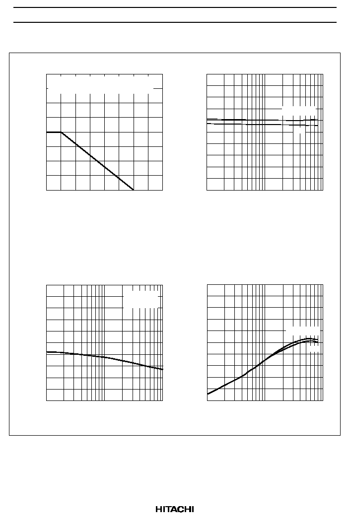
Main Characteristics
400
300
200
100
0
50
100
150
200
10
0.1
1
10
1
2
5
10
20
50
100
0
4
8
12
16
20
100
200
0
1
20
100
Collector Power Dissipation Pc* (mW)
Ambient Temperature Ta (
∞
C)
Collector Power Dissipation Curve
Collector to Base Voltage V (V)
CB
Collector Output Capacitance Cob (pF)
Collector Output Capacitance vs.
Collector to Base Voltage
Collector Current I (mA)
C
DC Current Transfer Ratio h
FE
DC Current Transfet Ratio vs.
Collector Current
Collector Current I (mA)
C
Gain Bandwidth Prodfuct f (GHz)
T
Gain Bandwidth Product vs.
Collector Current
2
5
50
0.8
1.6
2.4
3.2
4.0
0
0.2
0.5
2
5
I = 0
f = 1 MHz
E
V = 5 V
CE
3 V
3 V
V = 5 V
CE
*when using aluminum ceramic board
(12.5 x 20 x 0.7 mm)
2SC5759
4
1
5
10
50
100
10
1
10
100
3
5
0
1
20
100
Power Gain PG (dB)
Power Gain vs. Collector Current
S Parameter |S | (dB)
Collector Current I (mA)
C
Noise Figure NF (dB)
Noise Figure vs. Collector Current
2
5
50
4
8
12
16
20
0
2
5
20
50
0
4
8
12
16
20
Collector Current I (mA)
C
2
20
4
2
1
21
21
2
S Parameter vs. Collector Current
21
Collector Current I (mA)
C
3 V
f = 900 MHz
V = 5 V
CE
V = 5 V
CE
3 V
V = 3 V
CE
5 V
f = 900 MHz
f = 1 GHz
2SC5759
5
10
5
4
3
2
1.5
1
.8
-2
-3
-4
-5
-10
.6
.4
.2
0
-.2
-.4
-.6
-.8
-1
-1.5
.2
.4
.6 .8 1
2
3 4 5
1.5
10
0
∞
30
∞
60
∞
90
∞
120
∞
150
∞
180
∞
-150
∞
-90
∞
-60
∞
-30
∞
-120
∞
30
∞
60
∞
90
∞
120
∞
150
∞
180
∞
-150
∞
-90
∞
-60
∞
-30
∞
-120
∞
10
5
4
3
2
1.5
1
.8
-2
-3
-4
-5
-10
.6
.4
.2
0
-.2
-.4
-.6
-.8
-1
-1.5
.2
.4
.6 .8 1
2
3 4 5
1.5
10
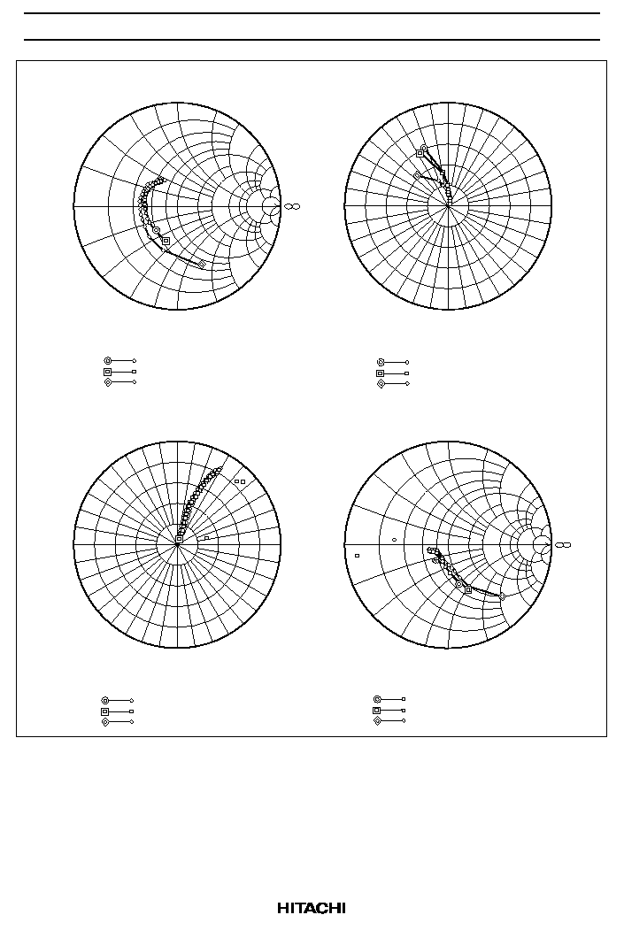
Scale: 10 / div.
Scale: 0.08 / div.
0
∞
Condition : V
CE
= 3 V, Zo = 50
100 to 2000 MHz (100 MHz Step)
Condition : V
CE
= 3 V, Zo = 50
100 to 2000 MHz (100 MHz Step)
Condition : V
CE
= 3 V, Zo = 50
100 to 2000 MHz (100 MHz Step)
Condition : V
CE
= 3 V, Zo = 50
100 to 2000 MHz (100 MHz Step)
:I
C
= 50 mA
:I
C
= 30 mA
:I
C
= 10 mA
:I
C
= 50 mA
:I
C
= 30 mA
:I
C
= 10 mA
:I
C
= 50 mA
:I
C
= 30 mA
:I
C
= 10 mA
:I
C
= 50 mA
:I
C
= 30 mA
:I
C
= 10 mA
S11 Parameter vs. Frequency
S12 Parameter vs. Frequency
S22 Parameter vs. Frequency
S21 Paramter vs. Frequency