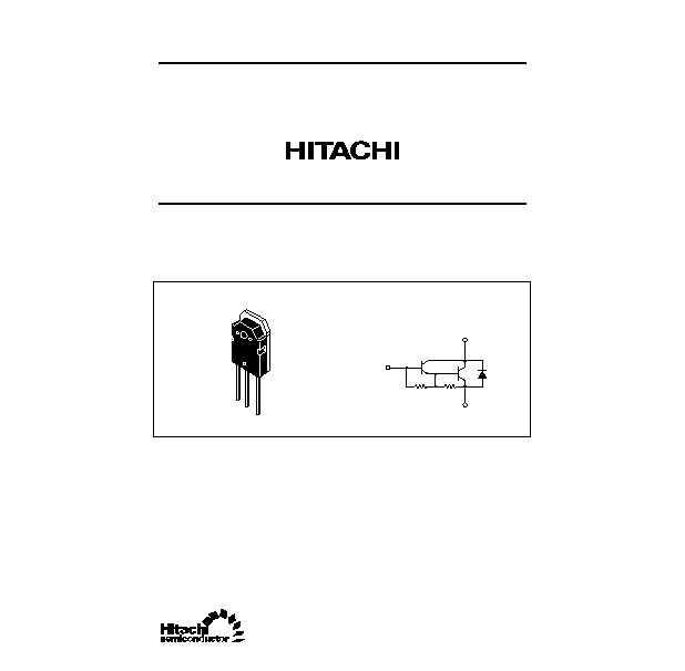
2SD1559
Silicon NPN Triple Diffused
Application
Low frequency power amplifier complementary pair with 2SB1079
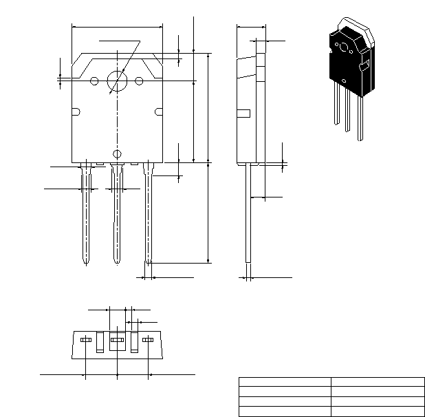
Outline
TO-3P
1. Base
2. Collector
(Flange)
3. Emitter
1
2
3
3 k
(Typ)
400
(Typ)
1
2
3
2SD1559
2
Absolute Maximum Ratings (Ta = 25∞C)
Item
Symbol
Ratings
Unit
Collector to base voltage
V
CBO
100
V
Collector to emitter voltage
V
CEO
100
V
Emitter to base voltage
V
EBO
7
V
Collector current
I
C
20
A
Collector peak current
I
C(peak)
30
A
Base current
I
B
3
A
Collector power dissipation
P
C
*
1
100
W
Junction temperature
Tj
150
∞
C
Storage temperature
Tstg
≠55 to +150
∞
C
Note:
1. Value at T
C
= 25
∞
C.
Electrical Characteristics (Ta = 25∞C)
Item
Symbol
Min
Typ
Max
Unit
Test conditions
Collector to base breakdown
voltage
V
(BR)CBO
100
--
--
V
I
C
= 0.1 mA, I
E
= 0
Collector to emitter breakdown
voltage
V
(BR)CEO
100
--
--
V
I
C
= 25 mA, R
BE
=
Collector to emitter sustain
voltage
V
CEO(sus)
100
--
--
V
I
C
= 200 mA, R
BE
=
*
1
Emitter to base breakdown
voltage
V
(BR)EBO
7
--
--
V
V
EB
= 50 mA, I
C
= 0
Collector cutoff current
I
CBO
--
--
100
µ
A
V
CB
= 100 V, I
E
= 0
I
CEO
--
--
1.0
mA
V
CE
= 80 V, R
BE
=
DC current transfer ratio
h
FE
1000
--
20000
V
CE
= 3 V, I
C
= 10 A*
1
Collector to emitter saturation
voltage
V
CE(sat)1
--
--
2.0
V
I
C
= 10 A, I
B
= 20 mA*
1
Base to emitter saturatiopn
voltage
V
BE(sat)1
--
--
2.5
V
Collector to emitter saturation
voltage
V
CE(sat)2
--
--
3.0
V
I
C
= 20 A, I
B
= 200 mA*
1
Base to emitter saturation
voltage
V
BE(sat)2
--
--
3.5
V
Turn on time
t
on
--
1.0
--
µ
s
I
C
= 10 A, I
B1
= ≠I
B2
= 20 mA
Storage time
t
stg
--
9.0
--
µ
s
Fall time
t
f
--
3.0
--
µ
s
Note:
1. Pulse test.

2SD1559
3
0
50
100
150
Case temperature T
C
(
∞
C)
Collector power dissipation Pc (W)
Maximum Collector Dissipation Curve
120
80
40
0.1
0.3
1
3
10
30
Collector to emitter voltage V
CE
(V)
Collector current I
C
(A)
1
3
10
30
100
300
Area of Safe Operation
10
µ
s
100
µ
s
PW = 10 ms
PW = 1 ms
DC (T
C
= 25
∞
C)
i
C
(peak)
I
C
(max)
Ta = 25
∞
C
1 shot pulse
Collector to emitter voltage V
CE
(V)
Collector current I
C
(A)
0
Typical Output Characteristics
1
2
3
4
5
4
8
12
16
20
T
C
= 25
∞
C
I
B
= 0.5 mA
1
3.5
2
3
4
1.5
2.5
30
100
300
1,000
3,000
10,000
30,000
Collector current I
C
(A)
DC current transfer ratio h
FE
0.3
1.0
3
10
30
DC Current Transfer Ratio
vs. Collector Current
V
CE
= 3 V
Pulse
T
C
= 75
∞
C
≠25
∞
C
25
∞
C

2SD1559
4
0.01
0.03
0.1
0.3
1.0
3
10
Collector current I
C
(A)
0.3
1.0
3
10
30
Collector to emitter saturation voltage V
CE
(sat)
(V)
Base to emitter saturation voltage V
BE
(sat)
(V)
Saturation Voltage vs. Collector Current
V
BE
(sat)
V
CE
(sat)
Ta = 25
∞
C
Pulse
500
500
l
C
/l
B
= 200
200
0.01
0.03
0.1
0.3
1.0
3
10
Collector current I
C
(A)
Switching time t (
µ
s)
0.3
1.0
3
10
30
Switching Time vs. Collector Current
V
CC
= 30 V
I
C
= 500 I
B1
= ≠500 I
B2
Ta = 25
∞
C
t
f
t
on
t
stg
0.01
0.03
0.1
0.3
1.0
3
10
Time t
Thermal resistance
j-c
(
∞
C/W)
0.1
100 (s)
10
1.0
0.1
100 (ms)
10
1.0
Transient Thermal Resistance
0.1 to 100 ms
T
C
= 25
∞
C
1 shot
0.1 to 100 s