 | –≠–ª–µ–∫—Ç—Ä–æ–Ω–Ω—ã–π –∫–æ–º–ø–æ–Ω–µ–Ω—Ç: 2SK1341 | –°–∫–∞—á–∞—Ç—å:  PDF PDF  ZIP ZIP |
2SK1299(L), 2SK1299(S)
Silicon N-Channel MOS FET
Application
High speed power switching
Features
∑
Low on-resistance
∑
High speed switching
∑
Low drive current
∑
4 V gate drive device
Can be driven from 5 V source
∑
Suitable for motor drive, DC-DC converter, power switch and solenoid drive
Outline
1
2
3
1
2 3
4
4
DPAK-1
1. Gate
2. Drain
3. Source
4. Drain
D
G
S

2SK1299(L), 2SK1299(S)
2
Absolute Maximum Ratings (Ta = 25∞C)
Item
Symbol
Ratings
Unit
Drain to source voltage
V
DSS
100
V
Gate to source voltage
V
GSS
±
20
V
Drain current
I
D
3
A
Drain peak current
I
D(pulse)
*
1
12
A
Body to drain diode reverse drain current
I
DR
3
A
Channel dissipation
Pch*
2
20
W
Channel temperature
Tch
150
∞
C
Storage temperature
Tstg
≠55 to +150
∞
C
Notes: 1. PW
10
µ
s, duty cycle
1%
2. Value at T
C
= 25
∞
C

2SK1299(L), 2SK1299(S)
3
Electrical Characteristics (Ta = 25∞C)
Item
Symbol Min
Typ
Max
Unit
Test conditions
Drain to source breakdown
voltage
V
(BR)DSS
100
--
--
V
I
D
= 10 mA, V
GS
= 0
Gate to source breakdown
voltage
V
(BR)GSS
±
20
--
--
V
I
G
=
±
100
µ
A, V
DS
= 0
Gate to source leak current
I
GSS
--
--
±
10
µ
A
V
GS
=
±
16 V, V
DS
= 0
Zero gate voltage drain current I
DSS
--
--
100
µ
A
V
DS
= 80 V, V
GS
= 0
Gate to source cutoff voltage
V
GS(off)
1.0
--
2.0
V
I
D
= 1 mA, V
DS
= 10 V
Static Drain to source on state
resistance
R
DS(on)
--
0.25
0.35
I
D
= 2 A, V
GS
= 10 V *
1
--
0.30
0.45
I
D
= 2 A, V
GS
= 4 V
1
*
Forward transfer admittance
|yfs|
2.4
4.0
--
S
I
D
= 2 A, V
DS
= 10 V *
1
Input capacitance
Ciss
--
400
--
pF
V
DS
= 10 V, V
GS
= 0,
Output capacitance
Coss
--
165
--
pF
f = 1 MHz
Reverse transfer capacitance
Crss
--
45
--
pF
Turn-on delay time
t
d(on)
--
5
--
ns
I
D
= 2 A, V
GS
= 10 V,
Rise time
t
r
--
35
--
ns
R
L
= 15
Turn-off delay time
t
d(off)
--
160
--
ns
Fall time
t
f
--
60
--
ns
Body to drain diode forward
voltage
V
DF
--
1.0
--
V
I
F
= 3 A, V
GS
= 0
Body to drain diode reverse
recovery time
t
rr
--
135
--
ns
I
F
= 3 A, V
GS
= 0,
di
F
/dt = 50 A/
µ
s
Note:
1. Pulse test
2SK1299(L), 2SK1299(S)
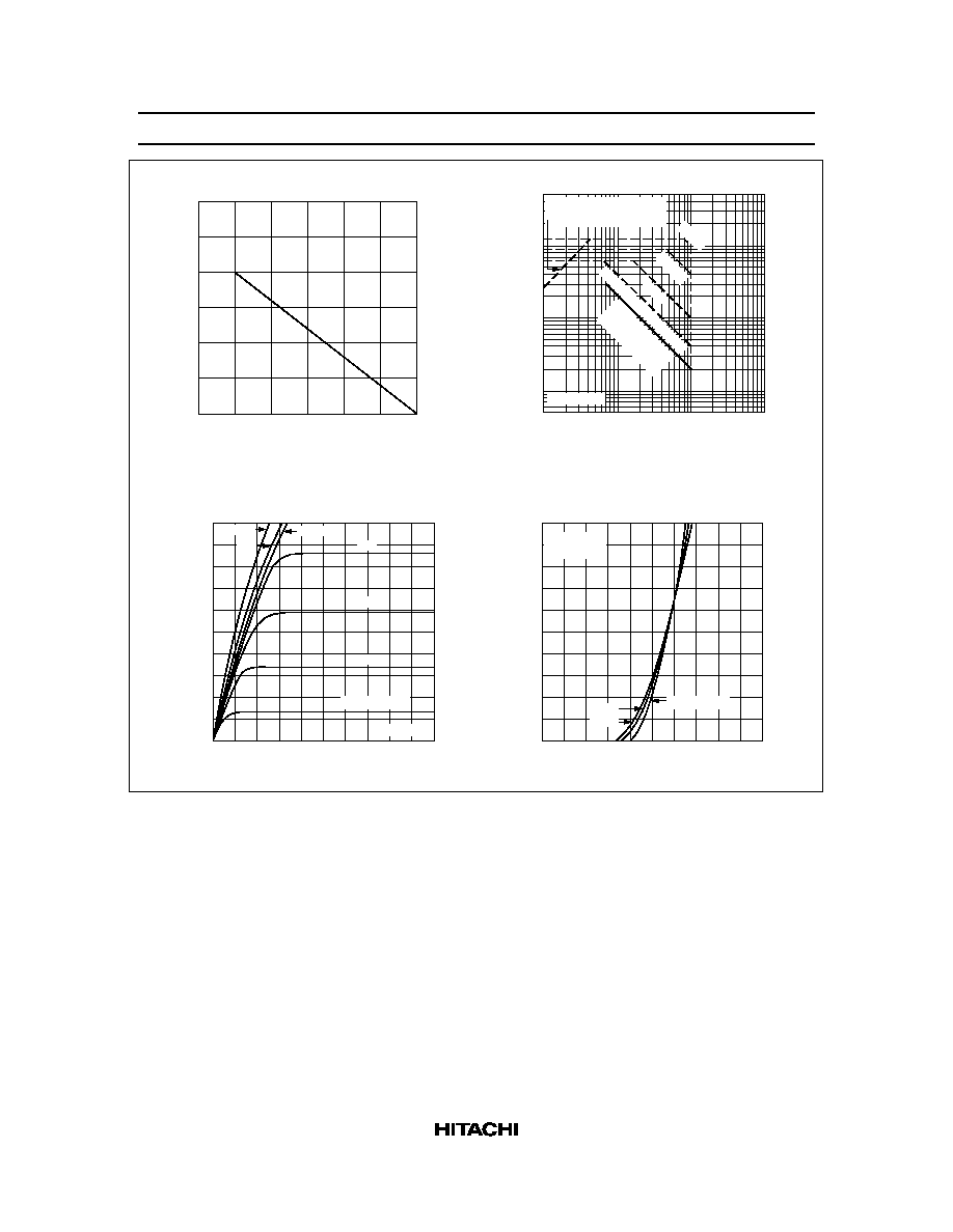
4
50
100
0
Case Temperature T
C
(∞C)
150
10
Channel Dissipation Pch
(W)
Power vs. Temperature Derating
20
30
Maximum Safe Operation Area
Drain Current I
D
(A)
500
100
20
5
2
50
10
5
2
0.2
1
20
1
0.5
0.1
0.05
200
Drain to Source Voltage V
DS
(V)
100
µ
s
1 ms
Ta = 25∞C
10
µ
s
Operation in this area
is limited by R
DS (on)
DC Operation
(T
C
= 25∞C)
PW = 10 ms (1 Shot)
10
50
1000
Typical Output Characteristics
Drain to Source Voltage V
DS
(V)
Drain Current I
D
(A)
10
8
6
4
2
10
8
6
4
2
0
V
GS
= 2.5 V
Pulse Test
5 V
3 V
3.5 V
10 V
4.5 V
4 V
Typical Transfer Characteristics
3
Gate to Source Voltage V
GS
(V)
4
2
1
0
5
1
2
3
4
5
0
Drain Current I
D
(A)
V
DS
= 10 V
Pulse Test
25∞C
75∞C
T
C
= ≠25∞C
2SK1299(L), 2SK1299(S)
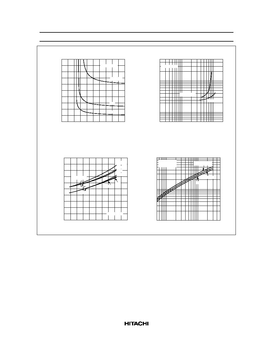
5
Drain to Source Saturation Voltage
vs. Gate to Source Voltage
6
Gate to Source Voltage V
GS
(V)
8
4
2
0
10
0.8
1.2
1.6
2.0
0
0.4
Drain to Source Saturation Voltage
V
DS
(on)
(V)
Pulse Test
I
D
= 5 A
2 A
1 A
2
Drain Current I
D
(A)
5
1
0.5
20
0.2
0.5
1
2
5
0.2
0.1
0.05
10
Static Drain to Source on State
Resistance vs. Drain Current
Static Drain to Source on State Resistance
R
DS
(on)
(
)
V
GS
= 4 V
10 V
Pulse Test
80
Case Temperature T
C
(∞C)
120
40
0
0.1
0.2
0.3
0.4
0.5
≠40
0
160
Static Drain to Source on State
Resistance vs. Temperature
Static Drain to Source on State Resistance
R
DS
(on)
(
)
I
D
= 5 A
Pulse Test
V
GS
= 4 V
10 V
2 A
1 A
5 A
2 A
1 A
Forward Transfer Admittance
vs. Drain Current
10
5
2
1
0.5
0.2
0.05
1.0
0.2
0.5
1
5
Drain Current I
D
(A)
2
Forward Transfer Admittance
yfs
(S)
0.1
T
C
= ≠25∞C
V
DS
= 10 V
Pulse Test
25∞C
75∞C