 | –≠–ª–µ–∫—Ç—Ä–æ–Ω–Ω—ã–π –∫–æ–º–ø–æ–Ω–µ–Ω—Ç: 2SK2729 | –°–∫–∞—á–∞—Ç—å:  PDF PDF  ZIP ZIP |

2SK2729
Silicon N Channel MOS FET
High Speed Power Switching
ADE-208-455 A
2nd. Edition
Features
∑
Low on-resistance
∑
High speed switching
∑
Low drive current
∑
Avalanche ratings
Outline
TO≠3P
1. Gate
2. Drain
(Flange)
3. Source
1
2
3
D
G
S

2SK2729
2
Absolute Maximum Ratings (Ta = 25∞C)
Item
Symbol
Ratings
Unit
Drain to source voltage
V
DSS
500
V
Gate to source voltage
V
GSS
±
30
V
Drain current
I
D
20
A
Drain peak current
I
D(pulse)
*
1
80
A
Body to drain diode reverse drain current
I
DR
20
A
Avalanche current
I
AP
*
3
20
A
Avalanche energy
E
AR
*
3
22
mJ
Channel dissipation
Pch*
2
150
W
Channel temperature
Tch
150
∞
C
Storage temperature
Tstg
≠55 to +150
∞
C
Notes: 1. PW
10
µ
s, duty cycle
1 %
2. Value at Tc = 25
∞
C
3. Value at Tch = 25
∞
C, Rg
50

2SK2729
3
Electrical Characteristics (Ta = 25∞C)
Item
Symbol
Min
Typ
Max
Unit
Test Conditions
Drain to source breakdown
voltage
V
(BR)DSS
500
--
--
V
I
D
= 10mA, V
GS
= 0
Gate to source breakdown
voltage
V
(BR)GSS
±
30
--
--
V
I
G
=
±
100
µ
A, V
DS
= 0
Gate to source leak current
I
GSS
--
--
±
10
µ
A
V
GS
=
±
25V, V
DS
= 0
Zero gate voltege drain
current
I
DSS
--
--
10
µ
A
V
DS
= 500 V, V
GS
= 0
Gate to source cutoff voltage
V
GS(off)
2.5
--
3.5
V
I
D
= 1mA, V
DS
= 10V*
1
Static drain to source on state
resistance
R
DS(on)
--
0.24
0.29
I
D
= 10A, V
GS
= 10V*
1
Forward transfer admittance
|y
fs
|
9
15
--
S
I
D
= 10A, V
DS
= 10V*
1
Input capacitance
Ciss
--
3300
--
pF
V
DS
= 10V
Output capacitance
Coss
--
900
--
pF
V
GS
= 0
Reverse transfer capacitance Crss
--
120
--
pF
f = 1MHz
Total gate charge
Qg
--
55
--
nc
V
DD
= 400V
Gate to source charge
Qgs
--
14
--
nc
V
GS
= 10V
Gate to drain charge
Qgd
--
17
--
nc
I
D
= 20A
Turn-on delay time
t
d(on)
--
45
--
ns
V
GS
= 10V, I
D
= 10A
Rise time
t
r
--
140
--
ns
R
L
= 3
Turn-off delay time
t
d(off)
--
150
--
ns
Fall time
t
f
--
85
--
ns
Body to drain diode forward
voltage
V
DF
--
1.0
--
V
I
D
= 20A, V
GS
= 0
Body to drain diode reverse
recovery time
t
rr
--
400
--
ns
I
F
= 20A, V
GS
= 0
diF/ dt = 100A/
µ
s
Note:
1. Pulse test
2SK2729
4
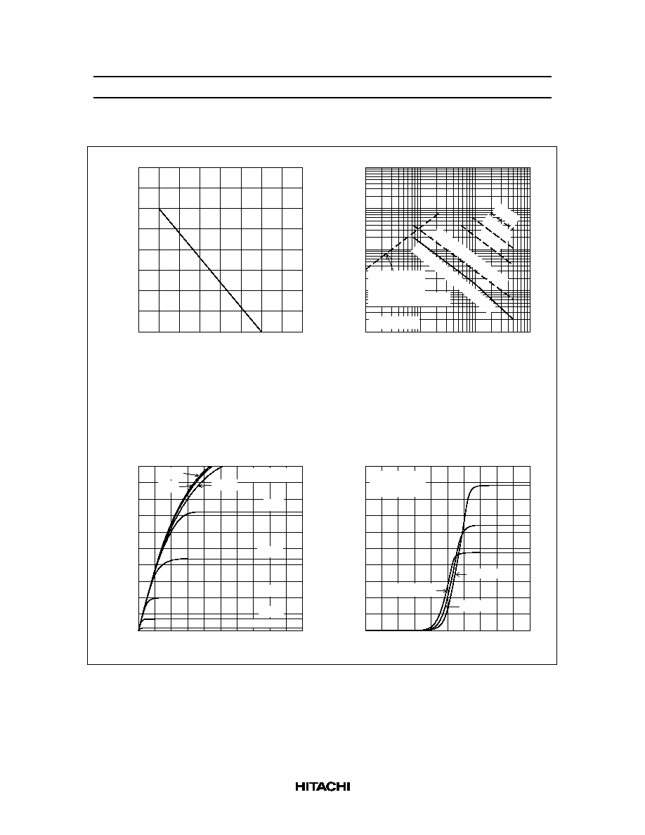
Main Characteristics
200
150
100
50
0
50
100
150
200
300
100
30
10
3
1
50
40
30
20
10
0
10
20
30
40
50
50
40
30
20
10
0
2
4
6
8
10
0.3
0.1
1000
Channel Dissipation Pch (W)
Case Temperature Tc (
∞
C)
Power vs. Temperature Derating
Drain to Source Voltage V (V)
DS
Drain Current I (A)
D
Maximum Safe Operation Area
Drain to Source Voltage V (V)
DS
Drain Current I (A)
D
Typical Output Characteristics
Gate to Source Voltage V (V)
GS
Drain Current I (A)
D
Typical Transfer Characteristics
10
µ
s
100
µ
s
1 ms
PW = 10 ms (1shot)
DC Operation (Tc = 25
∞
C)
Ta = 25
∞
C
Operation in
this area is
limited by R
DS(on)
V = 4 V
GS
6 V
5.5 V
4.5 V
5 V
10 V
8 V
6.5 V
Pulse Test
Tc = 75
∞
C
25
∞
C
≠25
∞
C
V = 10 V
Pulse Test
DS
1
3
10
30
100
300
1000

2SK2729
5
10
8
6
4
2
0
4
8
12
16
20
1
5
20
100
2
10
50
2
1
0.5
0.2
0.1
1.0
0.8
0.6
0.4
0.2
≠40
0
40
80
120
160
0
0.1 0.2
1
2
10 20
50
50
10
20
2
5
1
0.2
0.5
0.1
V = 10 V, 15 V
GS
0.5
5
Gate to Source Voltage V (V)
GS
Drain to Source Saturation Voltage vs.
Gate to Source Voltage
V (V)
DS(on)
Drain to Source Saturation Voltage
Drain Current I (A)
D
Drain to Source On State Resistance
R ( )
DS(on)
Static Drain to Source on State Resistance
vs. Drain Current
Case Temperature Tc (
∞
C)
R ( )
DS(on)
Static Drain to Source on State Resistance
Static Drain to Source on State Resistance
vs. Temperature
Drain Current I (A)
D
Forward Transfer Admittance |y | (S)
fs
Forward Transfer Admittance vs.
Drain Current
Pulse Test
Pulse Test
I = 20 A
D
V = 10 V
GS
10 A
5 A
25
∞
C
Tc = ≠25
∞
C
75
∞
C
I = 20 A
D
10 A
5 A
Pulse Test
V = 10 V
Pulse Test
DS