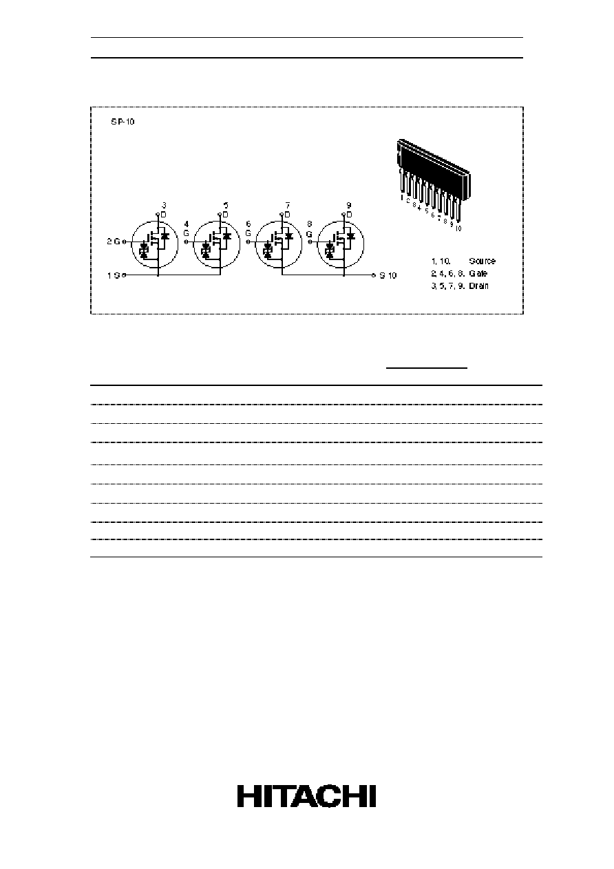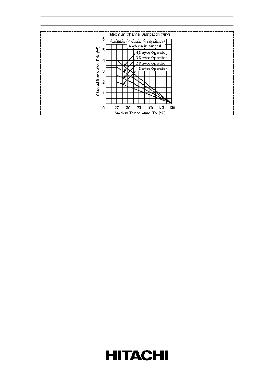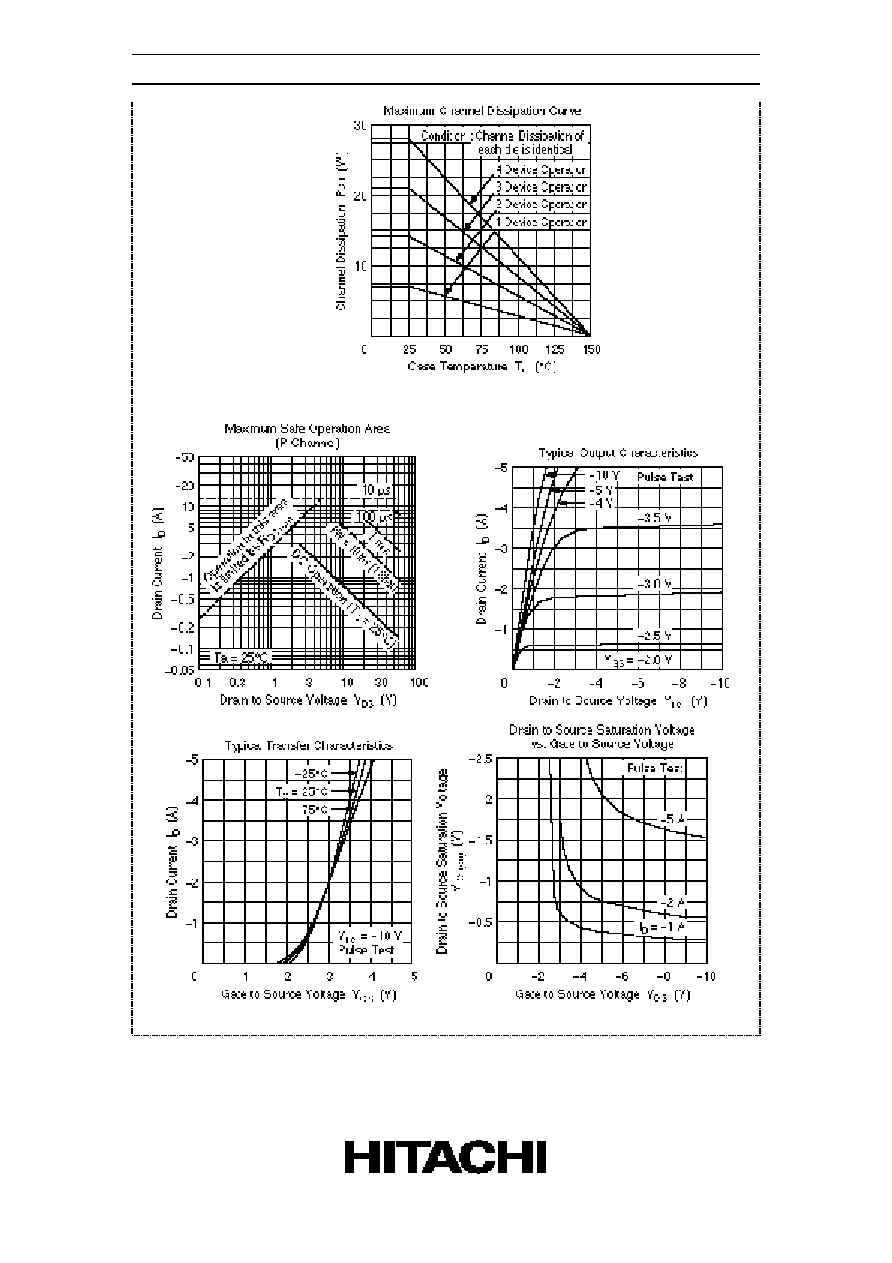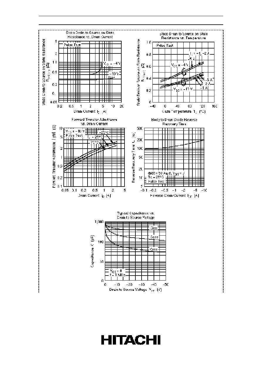
4AM13
Silicon N-Channel/P-Channel Power MOS FET Array
Application
High speed power switching
Features
∑
Low on-resistance
N-channel: RDS(on)
0.4
, VGS = 10 V, ID = 1.5 A
P-channel: RDS(on)
0.45
, VGS = ≠10 V, ID = ≠1.5 A
∑
Capable of 4 V gate drive
∑
Low drive current
∑
High speed switching
∑
High density mounting
∑
Suitable for H-bridged motor driver
4AM13
3
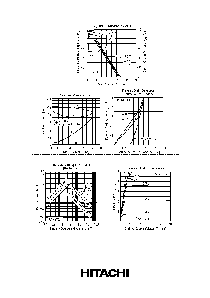
Electrical Characteristics (Ta = 25∞C) (1 Unit)
N channel
P channel
Item
Symbol
Min
Typ
Max
Min
Typ
Max
Unit
Test conditions
Drain to source
breakdown voltage
V(BR)DS
S
60
--
--
≠60
--
--
V
ID = 10 mA, VGS = 0
Gate to source
breakdown voltage
V(BR)GS
S
±20
--
--
±20
--
--
V
IG = ±100 µA, VDS =
0
Gate to source leak
current
IGSS
--
--
±10
--
--
±10
µA
VGS = ±16 V, VDS =
0
Zero gate voltage drain
current
IDSS
--
--
250
--
--
≠250
µA
VDS = 50 V, VGS = 0
Gate to source cutoff
voltage
VGS(off) 1.0
--
2.0
≠1.0
--
≠2.0
V
ID = 1 mA, VDS = 10
V
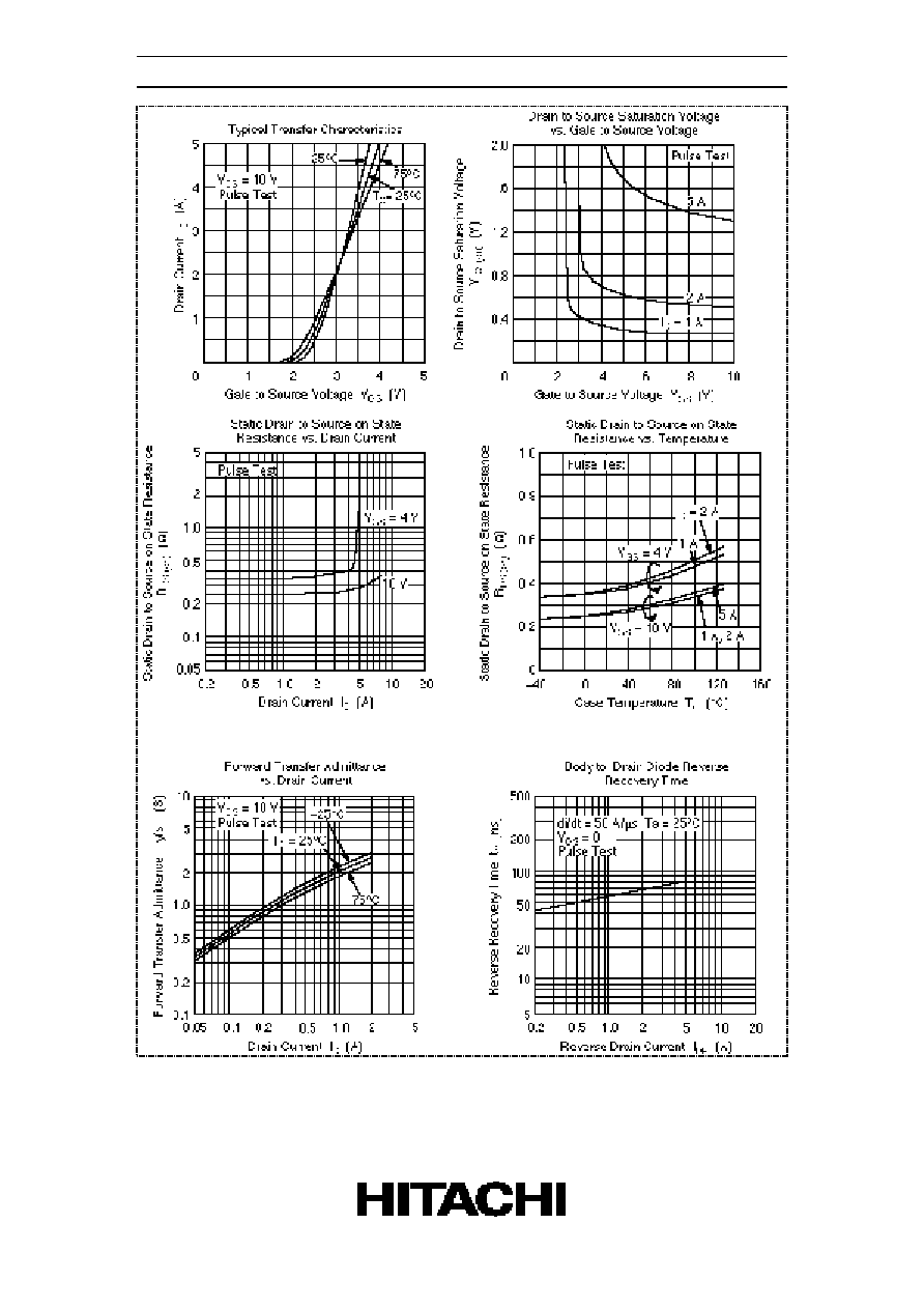
Static drain to source on
state resistance
RDS(on) --
0.25
0.35
--
0.28
0.4
ID = 1.5 A,
VGS = 10 V*
1
--
0.35
0.5
--
0.4
0.55
ID = 1.5 A, VGS = 4
V*1
Forward transfer
admittance
|yfs|
1.5
2.5
--
1.5
2.5
--
S
ID = 1.5 A,
VDS = 10 V*
1
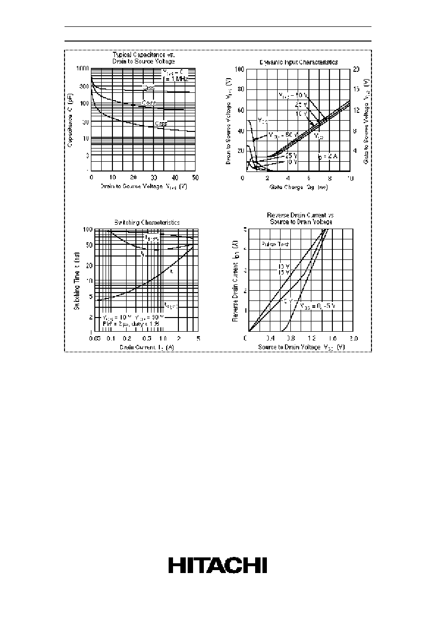
Input capacitance
Ciss
--
240
--
--
400
--
pF
VDS = 10 V, VGS = 0,
Output capacitance
Coss
--
115
--
--
240
--
pF
f = 1 MHz
Reverse transfer
capacitance
Crss
--
35
--
--
70
--
pF
Turn-on delay time
td(on)
--
4
--
--
5
--
ns
ID = 1.5 A, VGS = 10
V,
Rise time
tr
--
20
--
--
25
--
ns
RL = 20
Turn-off delay time
td(off)
--
80
--
--
180
--
ns
Fall time
tf
--
40
--
--
80
--
ns
Body to drain diode
forward voltage
VDF
--
1.2
--
--
≠1.1
--
V
IF = 3 A, VGS = 0
Body to drain diode
reverse recovery time
trr
--
75
--
--
140
--
ns
IF = 3 A, VGS = 0,
dIF/dt = 50 A/µs
Note:
1. Pulse Test
Polarity of test conditions for P channel device is reversed.
4AM13
10
When using this document, keep the following in mind:
1. This document may, wholly or partially, be subject to change without notice.
2. All rights are reserved: No one is permitted to reproduce or duplicate, in any form, the whole or
part of this document without Hitachi's permission.
3. Hitachi will not be held responsible for any damage to the user that may result from accidents or
any other reasons during operation of the user's unit according to this document.
4. Circuitry and other examples described herein are meant merely to indicate the characteristics and
performance of Hitachi's semiconductor products. Hitachi assumes no responsibility for any
intellectual property claims or other problems that may result from applications based on the
examples described herein.
5. No license is granted by implication or otherwise under any patents or other rights of any third
party or Hitachi, Ltd.
6. MEDICAL APPLICATIONS: Hitachi's products are not authorized for use in MEDICAL
APPLICATIONS without the written consent of the appropriate officer of Hitachi's sales company.
Such use includes, but is not limited to, use in life support systems. Buyers of Hitachi's products
are requested to notify the relevant Hitachi sales offices when planning to use the products in
MEDICAL APPLICATIONS.