 | –≠–ª–µ–∫—Ç—Ä–æ–Ω–Ω—ã–π –∫–æ–º–ø–æ–Ω–µ–Ω—Ç: BB301C | –°–∫–∞—á–∞—Ç—å:  PDF PDF  ZIP ZIP |
BB301C
Build in Biasing Circuit MOS FET IC
VHF RF Amplifier
ADE-208-507
1st. Edition
Features
∑
Build in Biasing Circuit; To reduce using parts cost & PC board space.
∑
Low noise characteristics; (NF = 1.3 dB typ. at f = 200 MHz)
∑
Withstanding to ESD; Build in ESD absorbing diode . Withstand up to 200 V at C = 200 pF,
Rs = 0 conditions.
Outline
1. Source
2. Gate1
3. Gate2
4. Drain
CMPAK≠4
1
4
3
2

BB301C
2
Absolute Maximum Ratings (Ta = 25∞C)
Item
Symbol
Ratings
Unit
Drain to source voltage
V
DS
6
V
Gate 1 to source voltage
V
G1S
+6
≠0
V
Gate 2 to source voltage
V
G2S
±
6
V
Drain current
I
D
25
mA
Channel power dissipation
Pch
100
mW
Channel temperature
Tch
150
∞
C
Storage temperature
Tstg
≠55 to +150
∞
C

BB301C
3
Electrical Characteristics (Ta = 25∞C)
Item
Symbol
Min
Typ
Max
Unit
Test conditions
Drain to source breakdown
voltage
V
(BR)DSS
6
--
--
V
I
D
= 200
µ
A
V
G1S
= V
G2S
= 0
Gate 1 to source breakdown
voltage
V
(BR)G1SS
+6
--
--
V
I
G1
= +10
µ
A
V
G2S
= V
DS
= 0
Gate 2 to source breakdown
voltage
V
(BR)G2SS
±
6
--
--
V
I
G2
=
±
10
µ
A
V
G1S
= V
DS
= 0
Gate 1 to source cutoff current I
G1SS
--
--
+100
nA
V
G1S
= +5 V
V
G2S
= V
DS
= 0
Gate 2 to source cutoff current I
G2SS
--
--
±
100
nA
V
G2S
=
±
5 V
V
G1S
= V
DS
= 0
Gate 1 to source cutoff voltage V
G1S(off)
0.4
--
1.0
V
V
DS
= 5 V, V
G2S
= 4 V
I
D
= 100
µ
A
Gate 2 to source cutoff voltage V
G2S(off)
0.4
--
1.0
V
V
DS
= 5 V, V
G1S
= 5 V
I
D
= 100
µ
A
Drain current
I
D(op)
10
15
20
mA
V
DS
= 5 V, V
G1
= 5 V
V
G2S
= 4 V, R
G
= 100 k
Forward transfer admittance
|y
fs
|
15
20
--
mS
V
DS
= 5 V, V
G1
= 5 V
V
G2S
= 4 V
R
G
= 100 k
, f = 1 kHz
Input capacitance
Ciss
2.2
3.0
4.0
pF
V
DS
= 5 V, V
G1
= 5 V
Output capacitance
Coss
0.9
1.2
1.6
pF
V
G2S
= 4 V, R
G
= 100 k
Reverse transfer capacitance
Crss
--
0.018
0.04
pF
f = 1 MHz
Power gain
PG
22
26
--
dB
V
DS
= 5 V, V
G1
= 5 V
V
G2S
= 4 V
Noise figure
NF
--
1.3
1.9
dB
R
G
= 100 k
, f = 200 MHz
Note:
Marking is "AW≠".
BB301C
4
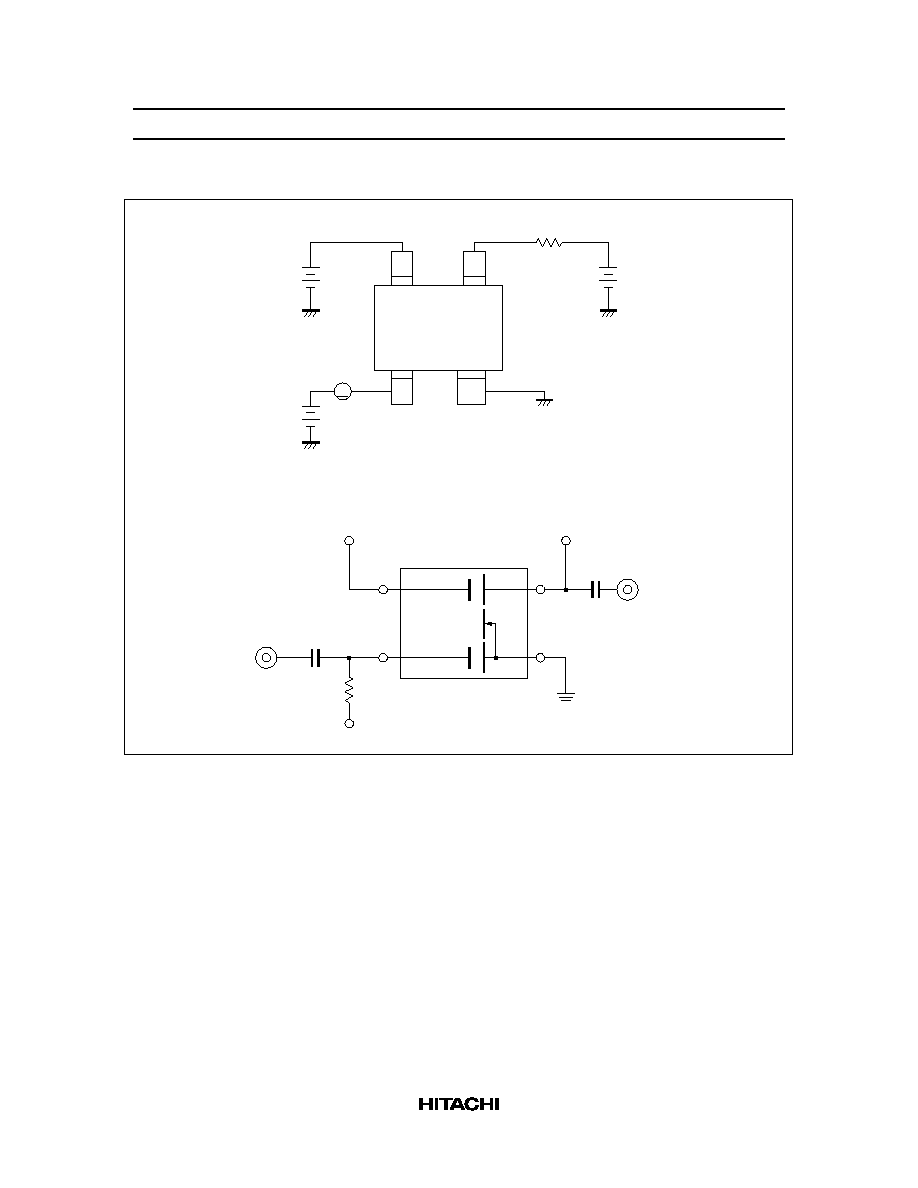
Main Characteristics
Test Circuit for Operating Items (I , |yfs|, Ciss, Coss, Crss, NF, PG)
Application Circuit
D(op)
Gate 1
Source
Drain
Gate 2
R
G
A
I
D
V
G2
V
G1
Output
Input
V = 4 to 0.3 V
AGC
V = 5 V
DS
R
G
V = 5 V
GG
BBFET
BB301C
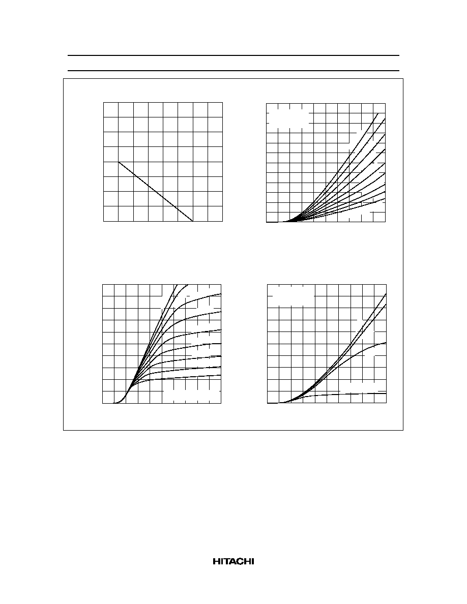
5
200
150
100
50
0
50
100
150
200
Channel Power Dissipation Pch (mW)
Ambient Temperature Ta (
∞
C)
Maximum Channel Power
Dissipation Curve
0
1
2
3
4
5
Drain to Source Voltage V
DS
(V)
Drain Current I
D
(mA)
Typical Output Characteristics
30
25
20
15
10
5
47 k
56 k
68 k
82 k
100 k
120 k
150 k
180 k
R = 220 k
G
V
G2S
= 4 V
V
G1
= V
DS
25
20
15
10
5
0
1
2
3
4
5
Drain Current I
D
(mA)
Gate2 to Source Voltage V
G2S
(V)
Drain Current vs.
Gate2 to Source Voltage
V
DS
= V
G1
= 5 V
120 k
100 k
82 k
68 k
R = 220 k
G
150 k
180 k
47 k
56 k
20
16
12
8
4
0
1
2
3
4
5
V
G2S
= 1 V
V
DS
= 5 V
R
G
= 82 k
4 V
3 V
2 V
Drain Current I
D
(mA)
Gate1 Voltage V
G1
(V)
Drain Current vs. Gate1 Voltage