PDE-3064-0
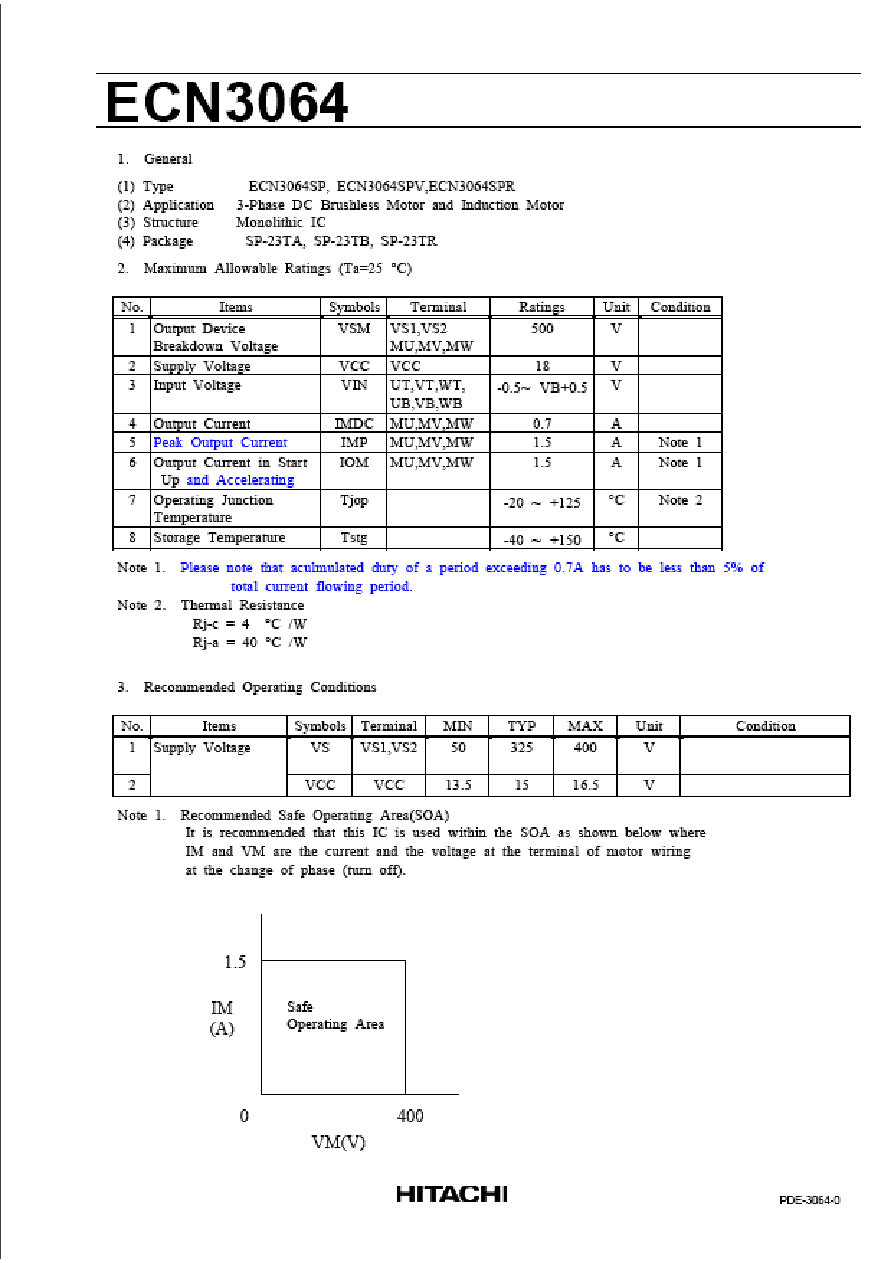
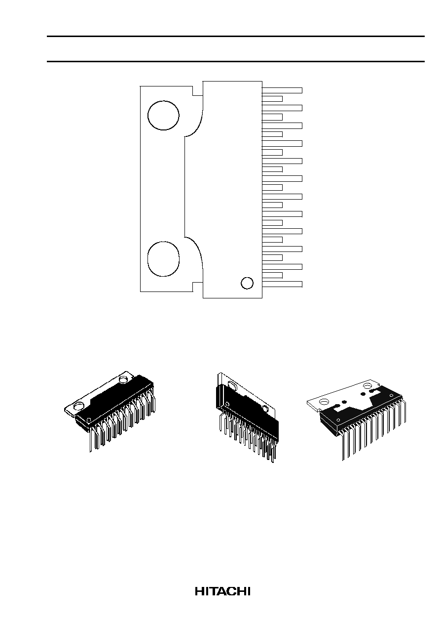
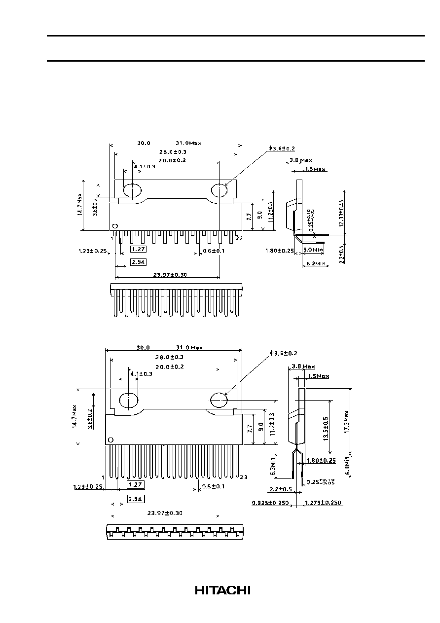
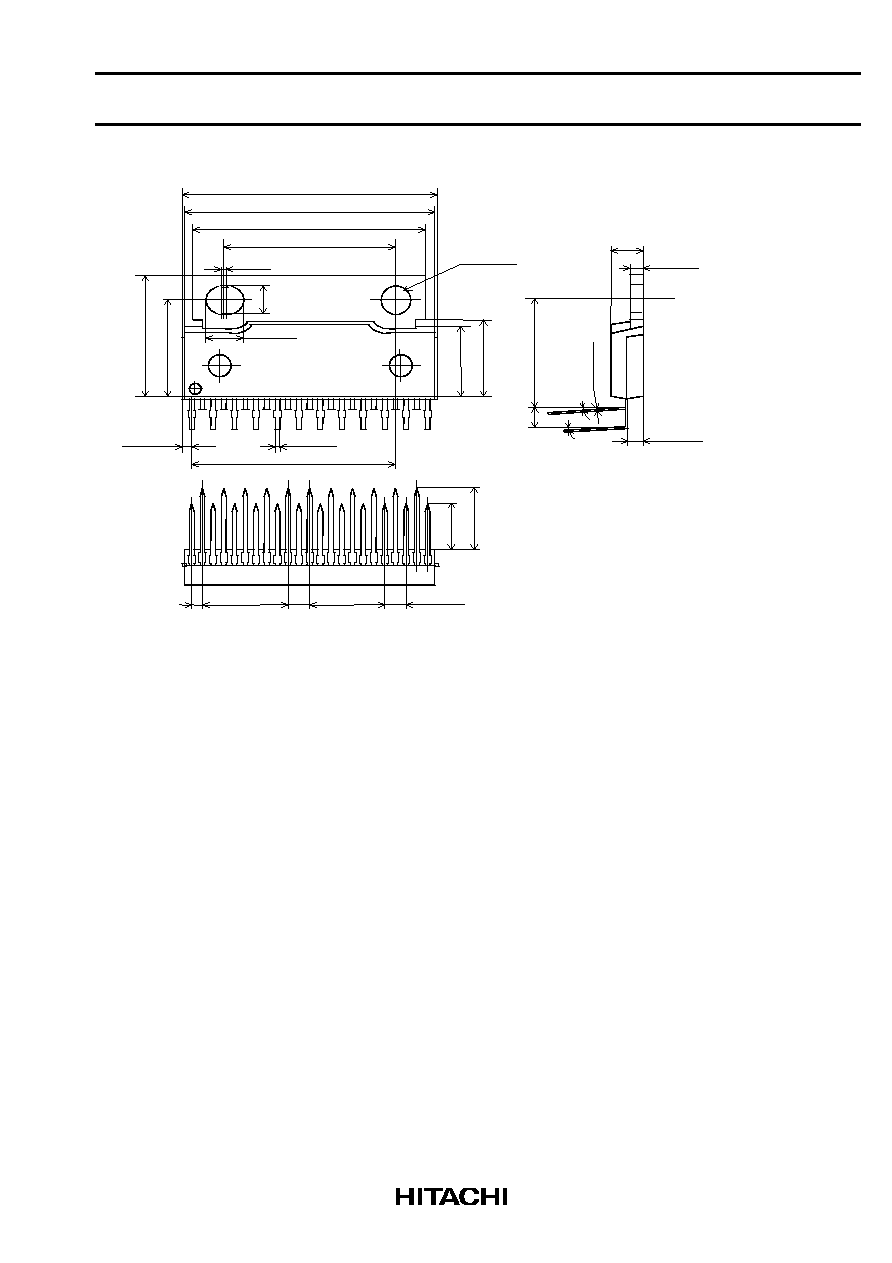
ECN3064
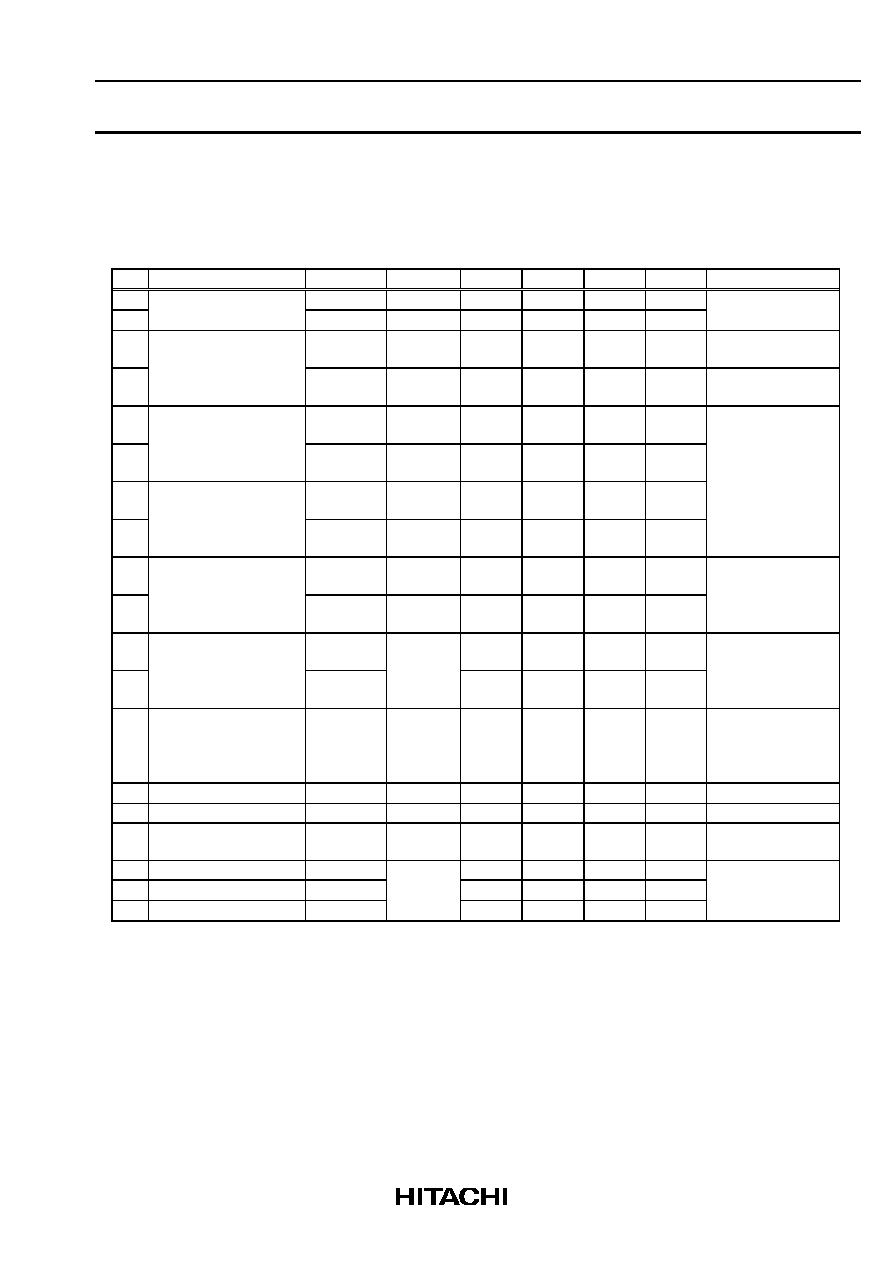
4. Electrical Characteristics (Ta=25
∞
C)
Unless otherwise specified, VCC=15V, VS=325V
Suffix T; Top arm B; Bottom arm
No.
Items
Symbols
Terminal
MIN
TYP
MAX
Unit
Condition
1
Standby Current
IS
VS1,VS2
-
0.5
1.5
mA
UT,VT,WT,UB,VB,
2
ICC
VCC
-
10
20
mA
WB=0V
3
Output device FVD
VFT
MU,MV,
MW
-
2.2
3.0
V
I=0.35A
4
VFB
MU,MV,
MW
-
2.2
3.0
V
I=0.35A
5
Turn On
TdONT
MU,MV,
MW
-
1.0
2.0
µ
s
6
Delay Time
TdONB
MU,MV,
MW
-
1.0
2.0
µ
s
I=0.35A
7
Turn Off
TdOFFT
MU,MV,
MW
-
1.0
2.0
µ
s
Resistive Load
8
Delay Time
TdOFFB
MU,MV,
MW
-
1.0
2.0
µ
s
9
Diode FVD
VFDT
MU,MV,
MW
-
2.2
2.8
V
I=0.35A
10
VFDB
MU,MV,
MW
-
2.4
3.0
V
11 Input Voltage
VIH
UT,VT,W
T,
3.5
-
-
V
12
VIL
UB,VB,W
B
-
-
1.5
V
13 Input Current
IIH
UT,VT,W
T,
UB,VB,W
B
-
-
100
µ
A
Input=5V Note 1
Pull Down Resistance
14 VB Output Voltage
VB
CB
6.8
7.5
8.2
V
15 VB Output Current
IB
CB
25
-
-
mA
deltaVLoad=0.1V
16 Reference Voltage
for Overcurrent
Vref
RS
0.45
0.5
0.55
V
17 LVSD Output Voltage LVSDON
VCC,MU,
10.0
11.5
12.9
V
Note.2
18 LVSD recover Voltage LVSDOFF MV,MW
10.1
12.0
13.0
V
19 LVSD reset hysterisis
Vrh
0.1
0.5
0.9
V
Note 1. Pull Down Resistance are typically 200 k
.
Note 2. LVSD : Low Voltage Shut Down
PDE-3064-0
ECN3064
5. Function
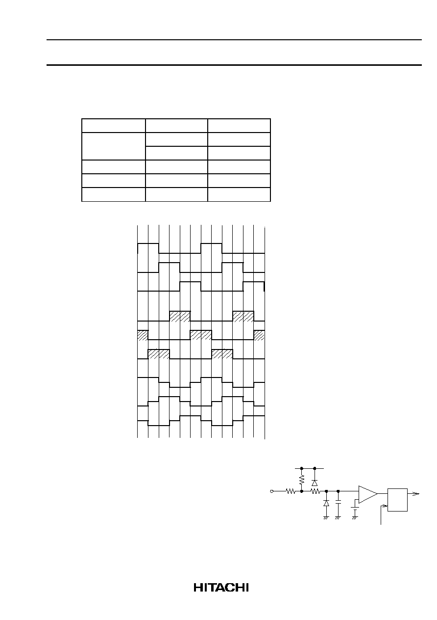
5.1 Truth Table
Terminal
Input
Output
UT,VT,WT,
L
OFF
UB,VB,WB
H
ON
UT,UB
UT&UB=H
OFF
VT,VB
VT&VB=H
OFF
WT,WB
WT&WB=H
OFF
5.2 Timing Chart
UT
VB
UB
WT
VT
WB
Top Arm
Bottom Arm
MU Output
MV Output
MW Output
Example of DC Brushless motor drive
5.3 Overcurrent Limiting Operation
This IC detects overcurrent by outside resistance Rs.
When Rs input voltage exceeds inner reference voltage
Vref(0.5V typical), this IC turns off the bottom output. After
overcurrent detection, a reset operation is done
at each inner clock signal period.
In case of not using this function, please connect Rs
terminal to GL terminal.
5pF
Vref
typ 220k
typ 200k
typ 300
VB
RS
RS terminal inner equvalent circuit
typ
Inner Clock Trigger
Latch
S
R

PDE-3064-0
ECN3064
6. Standard Application
Component
Recommended Value
Usage
Remark
C0
More than 0.22 uF
for inner power
supply(VB).
stress voltage is VB
C1,C2
1.0 uF
+/-
20%
for charge pump
stress voltage is VCC
D1,D2
Hitachi DFG1C6(Glass
mold type), DFM1F6
(Resin mold type)
or considerable parts
For charge pump
600V/1.0A
trr
100ns
CTR
1800 pF +/- 5%
for clock
Note 1.
RTR
22 k-ohm +/- 5%
for clock
Note 1.
Note 1. Clock frequency is determined
approximately
by next equation.
Floating capacitance of PCB must be considered.
At Recommended Value of CR, the error factor of IC is about 10%.
fclock = -1 / (2C*R*Ln(1-3.5/5.5)) ; Ln is natural logarithm
= 0.494 / (C*R) (Hz)
Clock
GH1
GL
VTR
CR
UT
VT
WT
UB
VB
WB
VCC
VS2
CL
C-
C+
CB
D2
D1
C1
C2
+
+
-
-
RS
CTR
RTR
VB
MU
MV
MW
VCC(15V)
Vref
VS
Top Arm
Driver
Bottom Arm
Driver
Pulse Generator
VB supply
Charge Pump
Microprocessor
Motor
VS1
GH2
C0
CLOCK
RS
Vref
0.5V
Latch
+
-
Filter
1
µ
s
R
S

1.
The information given herein, including the specifications and dimensions, is subject to
change without prior notice to improve product characteristics. Before ordering,
purchasers are adviced to contact Hitachi sales department for the latest version of this
data sheets.
2.
Please be sure to read "Precautions for Safe Use and Notices" in the individual brochure
before use.
3.
In cases where extremely high reliability is required(such as use in nuclear power control,
aerospace and aviation, traffic equipment, life-support-related medical equipment, fuel
control equipment and various kinds of safety equipment), safety should be ensured by
using semiconductor devices that feature assured safety or by means of users' fail-safe
precautions or other arrangement. Or consult Hitachi's sales department staff.
4.
In no event shall Hitachi be liable for any damages that may result from an accident or
any other cause during operation of the user's units according to this data sheets. Hitachi
assumes no responsibility for any intellectual property claims or any other problems that
may result from applications of information, products or circuits described in this data
sheets.
5.
In no event shall Hitachi be liable for any failure in a semiconductor device or any
secondary damage resulting from use at a value exceeding the absolute maximum rating.
6.
No license is granted by this data sheets under any patents or other rights of any third
party or Hitachi, Ltd.
7.
This data sheets may not be reproduced or duplicated, in any form, in whole or in part ,
without the expressed written permission of Hitachi, Ltd.
8.
The products (technologies) described in this data sheets are not to be provided to any
party whose purpose in their application will hinder maintenance of international peace
and safety not are they to be applied to that purpose by their direct purchasers or any
third party. When exporting these products (technologies), the necessary procedures are
to be taken in accordance with related laws and regulations.
HITACHI POWER SEMICONDUCTORS
For inquiries relating to the products, please contact nearest overseas representatives which is located
"Inquiry" portion on the top page of a home page.
Notices
Notices
Notices
Notices
Hitachi power semiconductor home page address http://www.hitachi.co.jp/pse