HA1127, HA1127P, HA1127FP
504
Absolute Maximum Ratings (Ta = 25∞C)
Item
Symbol
HA1127
Unit
Collector base voltage
V
CBO
20
V
Collector substrate voltage
V
CIO
20
V
Collector emitter voltage
V
CEO
15
V
Emitter-base voltage
V
EBO
5
V
Collector current
I
C
50
mA
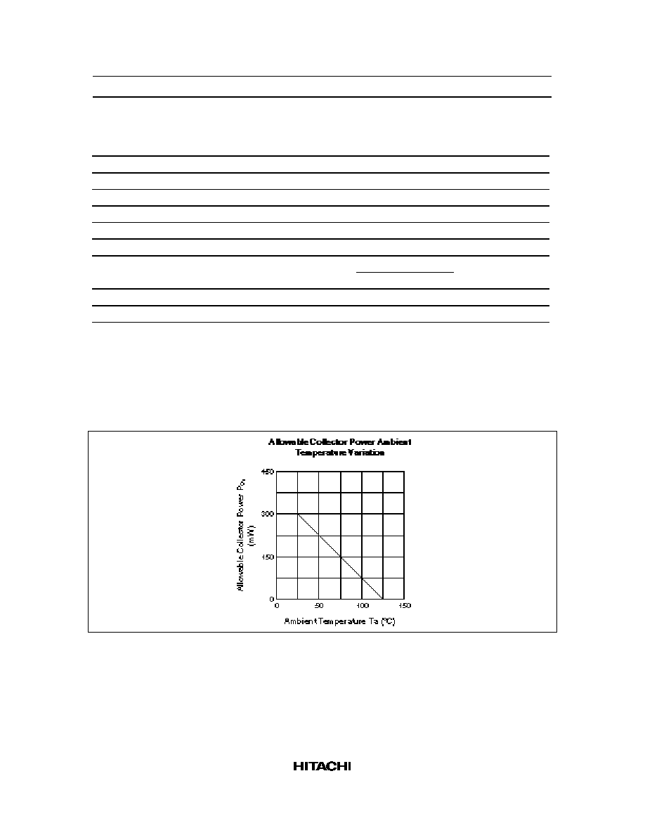
Allowable collector power
P
C
*
1
300
mW
Allowable collector power
P
C
750*
2
mW
625*
3
Operating temperature
Topr
≠55 to +125
∞C
Storage temperature
Tstg
≠55 to +125
∞C
Notes: 1. Allowable value per individual transistor. This is the allowable value up to Ta = 25∞C. Derate at
3 mW/∞C above that temperature.
2. Allowable value for the whole package.
This is the allowable value up to Ta = 35∞C for the HA1127P. Derate at 8.3 mW/∞C above that
temperature.
3. See page 51.

HA1127, HA1127P, HA1127FP
505
Electrical Characteristics (Ta = 25∞C)
Item
Symbol
Min
Typ
Max Unit
Test Condition
Collector-base
breakdown voltage
V
(BR)CBO
20
--
--
V
I
C
= 10 µA, I
E
= 0
Collector-emitter
breakdown voltage
V
(BR)CEO
15
--
--
V
I
C
= 1 mA, R
BE
=
Collector-substrate
breakdown voltage
V
(BR)CIO
20
--
--
V
I
C
= 10 µA, I
E
= 0, IB = 0
Emitter-base
breakdown voltage
V
(BR)EBO
5
--
--
V
I
E
= 10 µA, I
C
= 0
Collector cutoff
I
CBO
--
0.002 40
nA
V
CB
= 10 V, I
E
= 0
current
I
CEO
--
--
0.5
µA
V
CE
= 10 V, R
BE
=
Collector-emitter
saturation voltage
V
CE(sat)
--
0.17 --
V
I
C
= 10 mA, I
B
= 1 mA
Base-emitter
V
BE
--
0.72 --
V
V
CE
= 3 V
I
C
= 1 mA
voltage
--
0.80 --
V
I
C
= 10 mA
DC current
h
FE
40
140
--
V
EE
= 3 V
I
C
= 1 mA
amplification ratio
--
120
--
I
C
= 10 mA
Gain-bandwidth
product
f
T
--
460
--
MHz
V
CE
= 3 V, I
C
= 3 mA
Collector output
capacitance
Cob
--
1.7
--
pF
V
CB
= 3 V, I
E
= 0, f = 1 MHz
Emitter input
capacitance
Cin
--
2.0
--
pF
V
CB
= 3 V, I
E
= 0, f = 1 MHz
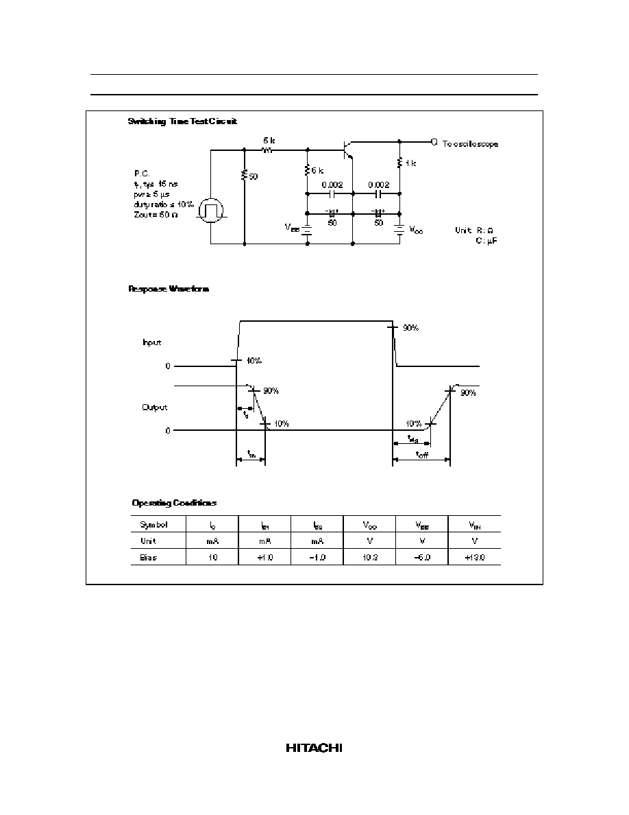
Switching time
t
on
--
35
--
ns
V
CC
= 10 V, I
C
= 10I
B1
= ≠10I
B2
= 10 mA
t
off
--
130
--
ns
t
stg
--
75
--
ns