 | –≠–ª–µ–∫—Ç—Ä–æ–Ω–Ω—ã–π –∫–æ–º–ø–æ–Ω–µ–Ω—Ç: HA12135AF | –°–∫–∞—á–∞—Ç—å:  PDF PDF  ZIP ZIP |

HA12134A, HA12135A, HA12136A
Dolby B-Type Noise Reduction System
ADE-207-016B (Z)
3rd Edition
Jun. 1999
Description
The HA12134A, HA12135A, HA12136A are silicon monolithic bipolar IC series providing dual channel
Dolby B-type noise reduction system* in one chip. The circuit is used primarily to reduce the level of
background noise introduced during recording and playback of audio signals on magnetic tape.
HA12134A series provide the following functions and features.
Functions
∑
Dual Dolby B-type NR processor
∑
NR ON/OFF control switch.
∑
Record (encode)/playback (decode) control switch.
Features
∑
Separate record/playback input and output.
Unprocessed signal output available in the encode and decode modes.
∑
Reduction of external components count.
∑
Small capacitor value for the reference voltage.
∑
NR ON/OFF switching and REC/PB switching are provided internally.
∑
2-type package (DP-16, FP-16DA)
∑
Wide range of operating supply voltage.
* Dolby is a trademark of Dolby Laboratories Licensing Corporation.
A license from Dolby Laboratories Licensing Corporation is required for the use of this IC.
HA12134A, HA12135A, HA12136A
2
Ordering Information
Type No
Dolby Level (mVrms)
Package
HA12134A
300
DP-16
HA12134AF
FP-16DA
HA12135A
450
DP-16
HA12135AF
FP-16DA
HA12136A
580
DP-16
HA12136AF
FP-16DA
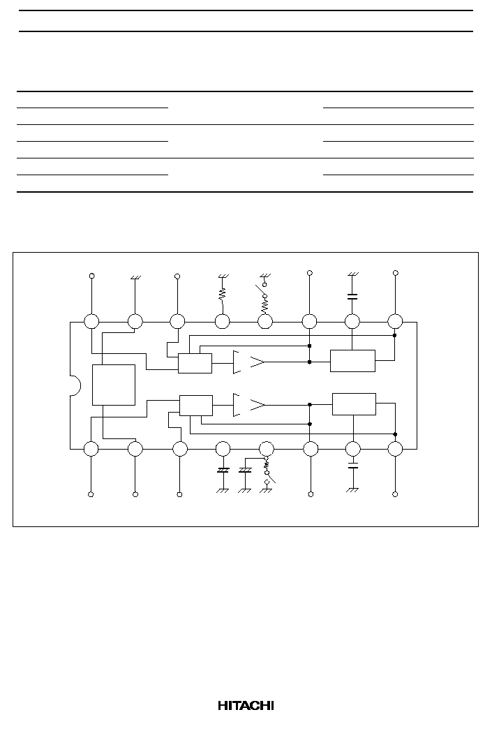
Block Diagram
GND
+
BIAS
SW
BUF
AMP
BUF
AMP
SW
SIDE
CHAIN
SIDE
CHAIN
16
15
14
13
12
11
10
9
8
7
6
5
4
3
2
1
REC IN
V
PB IN
V
NR
ON/OFF
REF
+
22
µ
0.22
µ
22 k
PB OUT
DET
REC OUT
REC OUT
0.22
µ
DET
PB OUT
22 k
18 k
REC/PB
BIAS
PB IN
REC IN
CC
1
µ

HA12134A, HA12135A, HA12136A
3
Absolute Maximum Ratings (Ta = 25
∞
C, Unless otherwise specified.)
Item
Symbol
Rating
Unit
Note
Supply voltage
Vccmax
16
V
Power dissipation
Pd
250
mW
Ta
85
∞
C
Operating temperature
Topr
≠40 to +85
∞
C
Storage temperature
Tstg
≠55 to +125
∞
C
Lead temperature
TI
260
∞
C
Note 1
Note:
1. Soldering 10 sec.

HA12134A, HA12135A, HA12136A
4
Electrical Characteristics (Ta = 25
∞
C, V
CC
= 12 V, Unless otherwise specified.)
Item
Symbol
Min
Typ
Max
Unit
Test conditions
Operating voltage
HA12134A Vope
6.5
12.0
16.0
V
Enable functional operations
HA12135A
8.0
12.0
16.0
HA12136A
9.5
12.0
16.0
Quiescent current
I
Q
--
7
--
mA
No signal, REC NR-ON
Voltage gain of
HA12134A G
VIA
21.0
23.0
25.0
dB
Pin 1
Pin 6
input amp
HA12135A
24.5
26.5
28.5
(Pin 16
Pin 11)
HA12136A
26.5
28.5
30.5
Vout = 0 dB, f = 1 kHz
NR encode boost
V 8 (9) (NR ON)
ENC-1.4
k (1)
2.9
4.4
5.9
dB
f = 1.4 kHz
V 8 (9) (NR OFF) = ≠20 dB
V 8 (9) (NR OFF)
ENC-1.4
k (2)
6.0
7.5
9.0
dB
f = 1.4 kHz
V 8 (9) (NR OFF) = ≠30 dB
ENC-5 k
(1)
1.7
3.2
4.7
dB
f = 5 kHz
V 8 (9) (NR OFF) = ≠20 dB
ENC-5 k
(2)
6.7
8.2
9.7
dB
f = 5 kHz
V 8 (9) (NR OFF) = ≠30 dB
ENC-10 k
(1)
≠1.1
0.4
1.9
dB
f = 10 kHz
V 8 (9) (NR OFF) = 0 dB
ENC-10 k
(2)
9.8
10.4
11.8
dB
f = 10 kHz
V 8 (9) (NR OFF) = ≠40 dB
T.H.D (REC)
T.H.D
(REC)
--
0.05
0.3
%
f = 1 kHz
V 8 (9) (NR ON) = 0 dB
Signal handling
HA12134A Vomax
12.0
13.0
--
dB
f = 1 kHz,
V
CC
= 6.5 V
HA12135A (REC)
T.H.D = 1%
V
CC
= 8.0 V
HA12136A
V
CC
= 9.5 V
Signal/noise ratio
(REC)
S/N
(REC)
62.0
68.0
--
dB
Rg = 5.1 k
weighted
CCIR/ARM
Crosstalk (ENC)
(Pin 8 ≠ Pin 9)
CT R
L
L
R
52.0
60.0
--
dB
f = 1 kHz
NR OFF
Control voltage for
REC/PB
REC
2.5
--
V
CC
V
REC/PB
22 k
Measure
12
PB
0.0
--
0.5
Control voltage for
NR ON/OFF
ON
2.5
--
V
CC
V
22k
Measure
NR
ON/OFF
5
OFF
0.0
--
0.5
Channel balance
G
VIA
≠1.0
0.0
1.0
dB

HA12134A, HA12135A, HA12136A
5
Electrical Characteristics (Ta = 25
∞
C, V
CC
= 12 V, Unless otherwise specified.) (cont)
Item
Symbol
Min
Typ
Max
Unit
Test conditions
Offset voltage
V 8 (9) (NR-ON) ≠
V 8 (9) (NR-OFF)
Vorec
≠50
0.0
50
mV
REC mode
V
CC
= 16.0 V
Test Circuit
+
+
+
Notes: 1. Resistor tolerances are
±
1%
2. Capacitor tolerances are
±
1%
3. Unit R: C: F
REC
IN
16
15
14
13
12
11
10
9
8
7
6
5
4
3
1
GND
PB IN
BIAS
REC/
PB
PB
OUT
DET
REC
OUT
REC
IN
Vcc
PB IN
V
NR
ON/OFF
PB
OUT
DET
REC
OUT
AC VOLT
METER
HP 400E or
EQUIVALENT
DISTORTION
ANALYZER
HP339A or
EQUIVALENT
OSCILLOSCOPE
TEKTRO 475 or
EQUIVALENT
NOISE METER
WITH CCIR/
ARM FILTER
DC POWER
SOURCE
AUDIO SG
HP339A or
EQUIVALENT
SW2
OFF
ON
R10
10k
SW9
0.68
µ
C11
C12
P
R
1
µ
R11
5.1k
R
L
R1
5.1k
SW1
SW3
R2
10k
0.68
µ
1
µ
+
+
+
+
OFF
ON
SW10
C3
100
µ
C4
1
µ
ON
OFF
SW4
C13
22
µ
R3
22k
C5
0.22
µ
+
+
C7
C6
10
µ
10
µ
R4
10k
SW5
R
P
P
R
SW6
R6
10k
+
+
R
P
SW7
R7
10k
C9
C10
0.22
µ
R8
22k
SW8
PB
REC
R9
18k
To Vcc
2
REF
10
µ
10
µ
C8
C1
C2
R5
10k
HA12134A, HA12135A, HA12136A
6
Pin Description (Ta = 25
∞
C, V
CC
= 12 V, No signal, The value in the table show typical
value.)
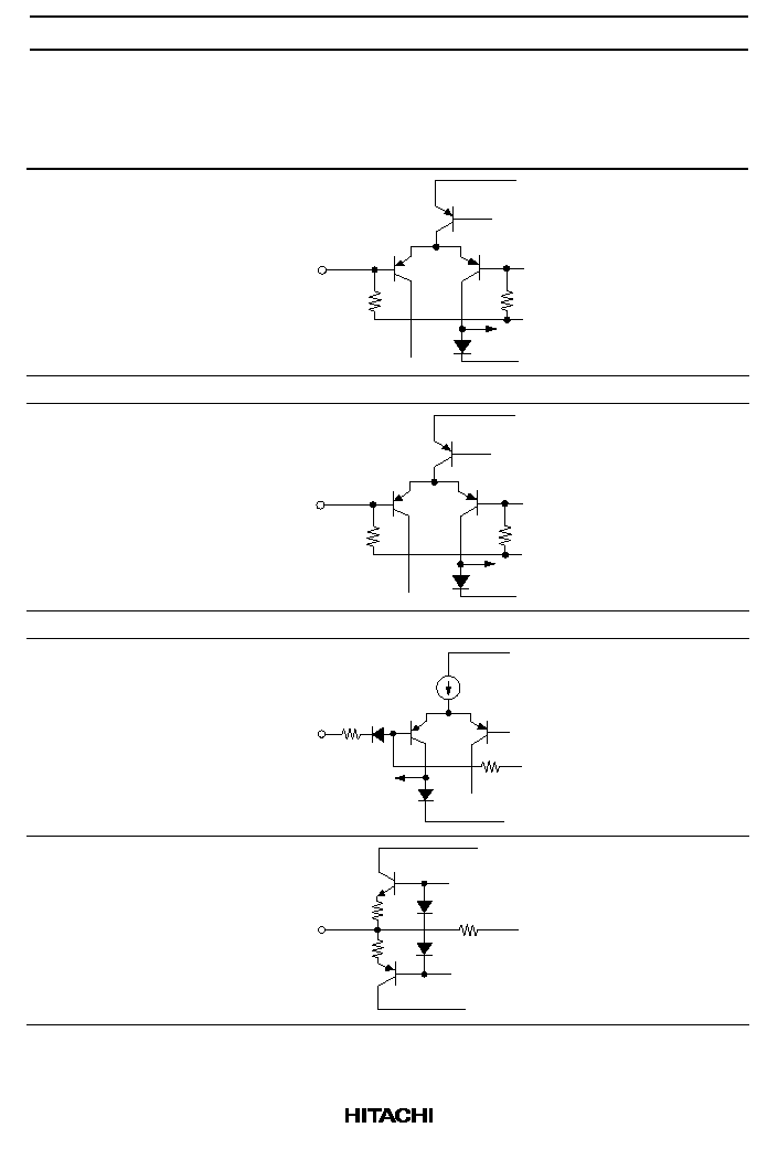
Pin No. Symbol
R (in)
VDC
Equivalent circuit
Description
1, 16
REC IN
56 k
6.0 V
V
GND
V /2
56k
CC
CC
Recording (encode) input
2
V
CC
--
12.0 V
Power supply
3, 14
PB IN
100 k
6.0 V
V
GND
V /2
100k
CC
CC
Playback (decode) input
4
V
REF
--
6.0 V
Reference voltage
5
NR ON/OFF --
--
V
4 V
BE
3 V
BE
GND
1k
CC
100k
Mode control pin for NR
ON/OFF
"H"
NR ON
"L"
NR OFF
6, 11
PB OUT
--
6.0 V
V
GND
100
100
CC
Playback (decode) output

HA12134A, HA12135A, HA12136A
7
Pin Description (Ta = 25
∞
C, V
CC
= 12 V, No signal, The value in the table show typical
value.) (cont)
Pin No. Symbol
R (in)
VDC
Equivalent circuit
Description
7, 10
DET
--
1.3 V
GND
V
CC
Time constant pin for the
level detector
8, 9
REC OUT
--
6.0 V
V
GND
100
100
CC
Recording (encode)
output
12
REC/PB
--
--
V
4 V
BE
3 V
BE
GND
1k
CC
100k
Mode control pin for
REC/PB (encode/decode)
"H"
REC (encode)
"L"
PB (decode)
13
BIAS
--
1.0 V
V
GND
CC
Reference current input
pin for the active filters
15
GND
--
0 V
--
Ground
HA12134A, HA12135A, HA12136A
8
10
8
6
4
2
0
4
6
8
10
12
14
16
18
Supply voltage Vcc [V]
Quiescent current I [mA]
Q
No Signal
HA12134A/5A/6A
NR-ON
NR-OFF
Figure 1 Quiescent Current vs. Supply Voltage
3.0
2.5
2.0
1.5
1.0
0
4
6
8
10
12
14
16
18
Supply voltage Vcc [V]
Control voltage (REC/PB) [V]
0.5
HA12134A/5A/6A
REC Mode
PB Mode
Figure 2 REC/PB Control Voltage vs. Supply Voltage

HA12134A, HA12135A, HA12136A
9
3.0
2.5
2.0
1.5
1.0
0
4
6
8
10
12
14
16
18
Supply voltage Vcc [V]
Control voltage (NR-ON/OFF) [V]
0.5
HA12134A/5A/6A
NR-ON
NR-OFF
Figure 3 NR-ON/OFF Control Voltage vs. Supply Voltage
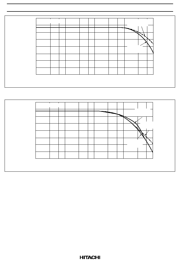
12
10
8
6
4
2
0
100 200
500
1 k
2 k
5 k
10 k 20 k
50 k
100 k
HA12136A
Frequency [Hz]
Encode boost [dB]
12 V
≠40 dB
9.5 V
≠30 dB
≠20 dB
≠10 dB
0 dB
16 V
Figure 4 Encode Boost vs. Frequency
HA12134A, HA12135A, HA12136A
10
100
300
600 1 k
3 k
6 k 10 k
30 k
60 k
Frequency [Hz]
100 k
300 k 600 k 1 M
0
10
20
30
Output gain Gv [dB]
HA12136A
PB Out
NR≠ON/OFF
REC Out
NR≠OFF
Figure 5 REC Mode Output Gain vs. Frequency
100
300
600 1 k
3 k
6 k 10 k
30 k
60 k
Frequency [Hz]
100 k
300 k 600 k 1 M
0
10
20
30
Output gain Gv [dB]
HA12136A
PB Out
NR≠OFF
REC Out
NR≠OFF
REC Out
NR≠ON
Figure 6 PB Mode Output Gain vs. Frequency

HA12134A, HA12135A, HA12136A
11
100
200
400
1 k
2 k
4 k
6 k
10 k
20 k
Frequency [Hz]
HA12136A
NR≠ON
NR≠OFF
≠40
≠30
≠20
≠10
0
Ripple rejection ratio R.R.R. [dB]
Figure 7 REC Mode Ripple Rejection Ratio vs. Frequency
100
200
400
1 k
2 k
4 k
10 k
20 k
Frequency [Hz]
HA12136A
NR≠ON
≠50
≠40
≠30
≠20
≠10
Ripple rejection ratio R.R.R. [dB]
NR≠OFF
Figure 8 PB Mode Ripple Rejection Ratio vs. Frequency
HA12134A, HA12135A, HA12136A
12
≠25
≠20
≠15
≠10
≠5
0
5
10
15
20
0.01
0.03
0.1
0.3
1.0
3
10
V [dB]
out
T.H.D. [%]
HA12136A
V = 12 V
1 kHz
100 Hz
10 kHz
CC
Figure 9 REC NR-OFF Total Harmonic Distortion vs. Output Level
≠25
≠20
≠15
≠10
≠5
0
5
10
15
20
0.01
0.03
0.1
0.3
1.0
3
10
V [dB]
out
T.H.D. [%]
HA12136A
V = 12 V
1 kHz
100 Hz
10 kHz
CC
Figure 10 REC NR-ON Total Harmonic Distortion vs. Output Level

HA12134A, HA12135A, HA12136A
13
≠25
≠20
≠15
≠10
≠5
0
5
10
15
20
0.01
0.03
0.1
0.3
1.0
3
10
V [dB]
out
T.H.D. [%]
HA12136A
V = 12 V
1 kHz
100 Hz
10 kHz
CC
Figure 11 PB NR-OFF Total Harmonic Distortion vs. Output Level
≠25 ≠20
≠15
≠10
≠5
0
5
10
15
20
0.01
0.03
0.1
0.3
1.0
3
10
V [dB]
out
T.H.D. [%]
HA12136A
V = 12 V
1 kHz
100 Hz
10 kHz
≠30
CC
Figure 12 PB NR-ON Total Harmonic Distortion vs. Output Level

HA12134A, HA12135A, HA12136A
14
20
19
18
17
16
15
13
14
12
11
10
8
9
10
11
12
13
14
15
16
Supply voltage V [V]
Maximum output level V [dB]
omax
HA12136A
PB NR-ON
REC NR-OFF
PB NR-OFF
REC NR-ON
CC
Figure 13 Maximum Output Level vs. Supply Voltage
90
85
80
75
70
Supply voltage V [V]
8
65
60
55
S/N [dB]
10
12
14
16
18
HA12136A
PB NR-ON
REC NR-OFF
PB NR-OFF
REC NR-ON
CC
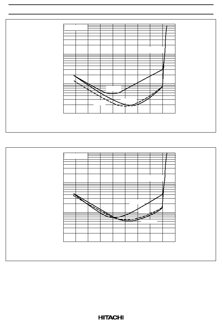
Figure 14 REC/PB Signal To Noise Ratio vs. Supply Voltage

HA12134A, HA12135A, HA12136A
15
12
10
8
6
4
2
0
100 200
500
1 k
2 k
5 k
10 k 20 k
50 k 100 k
HA12135A
Frequency [Hz]
Encode boost [dB]
12 V
≠40 dB
8.0 V
≠30 dB
≠20 dB
≠10 dB
0 dB
16 V
Figure 15 Encode Boost vs. Frequency
100
300
600 1 k
3 k
6 k 10 k
30 k
60 k
Frequency [Hz]
100 k
300 k 600 k 1 M
0
10
20
30
Output gain Gv [dB]
HA12135A
PB Out
NR≠ON/OFF
REC Out
NR≠OFF
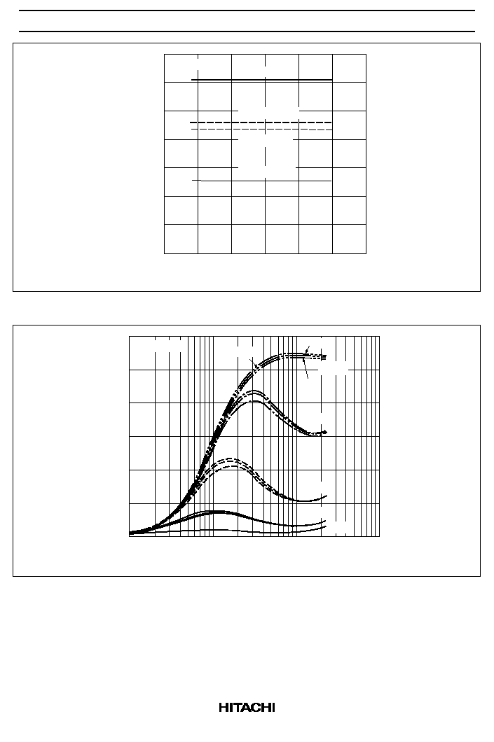
Figure 16 REC Mode Output Gain vs. Frequency

HA12134A, HA12135A, HA12136A
16
100
300
600 1 k
3 k
6 k 10 k
30 k
60 k
Frequency [Hz]
100 k
300 k 600 k 1 M
0
10
20
30
Output gain Gv [dB]
HA12135A
REC Out
NR≠OFF
PB≠Out
NR≠OFF
REC Out
NR≠ON
Figure 17 PB Mode Output Gain vs. Frequency
100
200
400
1 k
2 k
4 k
10 k
20 k
Frequency [Hz]
HA12135A
≠40
≠30
≠20
≠10
Ripple rejection ratio R.R.R. [dB]
≠50
NR≠OFF
NR≠ON
Figure 18 REC Mode Ripple Rejection Ratio vs. Frequency
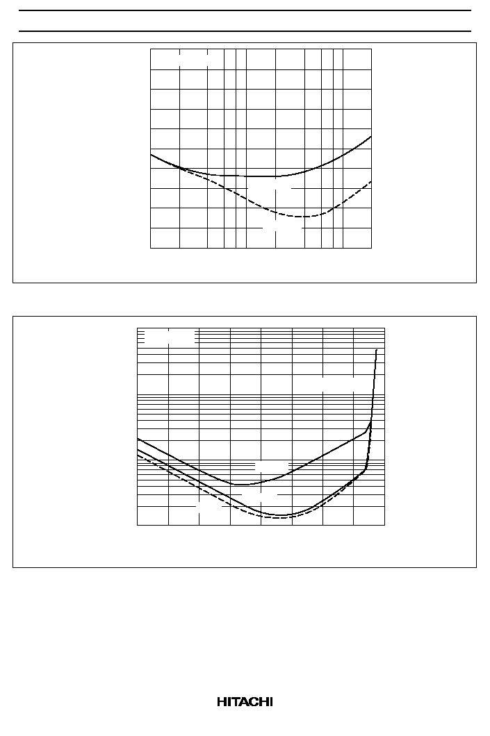
HA12134A, HA12135A, HA12136A
17
100
200
400
1 k
2 k
4 k
10 k
20 k
Frequency [Hz]
HA12135A
≠40
≠30
≠20
≠10
Ripple rejection ratio R.R.R. [dB]
≠50
NR≠OFF
NR≠ON
Figure 19 PB Mode Ripple Rejection Ratio vs. Frequency
≠20
≠15
≠10
≠5
0
5
10
15
20
0.01
0.03
0.1
0.3
1.0
3
10
V [dB]
out
T.H.D. [%]
HA12135A
V = 12 V
1 kHz
100 Hz
10 kHz
CC
Figure 20 REC NR-OFF Total Harmonic Distortion vs. Output Level

HA12134A, HA12135A, HA12136A
18
≠20
≠15
≠10
≠5
0
5
10
15
20
0.01
0.03
0.1
0.3
1.0
3
10
V [dB]
out
T.H.D. [%]
HA12135A
V = 12 V
1 kHz
100 Hz
10 kHz
CC
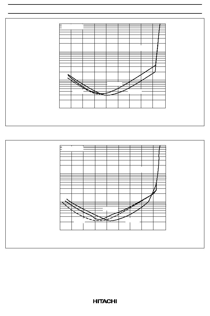
Figure 21 REC NR-ON total Harmonic Distortion vs. Output Level
≠20
≠15
≠10
≠5
0
5
10
15
20
0.01
0.03
0.1
0.3
1.0
3
10
V [dB]
out
T.H.D. [%]
HA12135A
V = 12 V
1 kHz
100 Hz
10 kHz
CC
Figure 22 PB NR-OFF Total Harmonic Distortion vs. Output Level

HA12134A, HA12135A, HA12136A
19
≠20
≠15
≠10
≠5
0
5
10
15
20
0.01
0.03
0.1
0.3
1.0
3
10
V [dB]
out
T.H.D. [%]
HA12135A
V = 12 V
1 kHz
100 Hz
10 kHz
CC
Figure 23 PB NR-ON Total Harmonic Distortion vs. Output Level
20
18
16
14
12
10
8
9
10
11
12
13
14
15
16
Supply voltage V [V]
Maximum output level V [dB]
omax
HA12135A
PB NR-ON
REC NR-OFF
PB NR-OFF
REC NR-ON
22
7
CC
Figure 24 Maximum Output Level vs. Supply Voltage
HA12134A, HA12135A, HA12136A
20
90
85
80
75
70
Supply voltage V [V]
8
65
60
55
S/N [dB]
10
12
14
16
18
HA12135A
PB NR-ON
REC NR-OFF
PB NR-OFF
REC NR-ON
6
CC
Figure 25 REC/PB Signal to Noise Ratio vs. Supply Voltage
12
10
8
6
4
2
0
100 200
500
1 k
2 k
5 k
10 k 20 k
50 k 100 k
HA12134A
Frequency [Hz]
Encode boost [dB]
12 V
≠40 dB
6.5 V
≠30 dB
≠20 dB
≠10 dB
0 dB
16 V
Figure 26 Encode Boost vs. Frequency

HA12134A, HA12135A, HA12136A
21
100
300 600 1 k
3 k
6 k 10 k
30 k 60 k
Frequency [Hz]
100 k
300 k 600 k 1 M
0
10
20
30
Output gain Gv [dB]
HA12134A
PB Out
NR≠ON/OFF
REC Out
NR≠OFF
Figure 27 REC Mode Output Gain vs. Frequency
100
300 600 1 k
3 k
6 k 10 k
30 k 60 k
Frequency [Hz]
100 k 300 k 600 k 1 M
0
10
20
30
Output gain Gv [dB]
HA12134A
PB Out
NR≠OFF
REC Out
NR≠OFF
REC Out
NR≠ON
Figure 28 PB Mode Output Gain vs. Frequency

HA12134A, HA12135A, HA12136A
22
100
200
400
1 k
2 k
4 k
10 k
20 k
Frequency [Hz]
HA12134A
≠40
≠30
≠20
≠10
Ripple rejection ratio R.R.R. [dB]
≠50
NR≠OFF
NR≠ON
Figure 29 REC Mode Ripple Rejection Ratio vs. Frequency
100
200
400
1 k
2 k
4 k
10 k
20 k
Frequency [Hz]
HA12134A
≠40
≠30
≠20
≠10
Ripple rejection ratio R.R.R. [dB]
≠50
NR≠OFF
NR≠ON
Figure 30 PB Mode Ripple Rejection Ratio vs. Frequency

HA12134A, HA12135A, HA12136A
23
≠20
≠15
≠10
≠5
0
5
10
15
20
0.01
0.03
0.1
0.3
1.0
3
10
V [dB]
out
T.H.D. [%]
HA12134A
V = 12 V
1 kHz
100 Hz
10 kHz
25
CC
Figure 31 REC NR-OFF Total Harmonic Distortion vs. Output Level
≠20
≠15
≠10
≠5
0
5
10
15
20
0.01
0.03
0.1
0.3
1.0
3
10
V [dB]
out
T.H.D. [%]
HA12134A
V = 12 V
1 kHz
100 Hz
10 kHz
25
CC
Figure 32 REC NR-ON Total Harmonic Distortion vs. Output Level
HA12134A, HA12135A, HA12136A
24
≠20
≠15
≠10
≠5
0
5
10
15
20
0.01
0.03
0.1
0.3
1.0
3
10
V [dB]
out
T.H.D. [%]
HA12134A
V = 12 V
1 kHz
100 Hz
10 kHz
25
CC
Figure 33 PB NR-OFF Total Harmonic Distortion vs. Output Level
≠20
≠15
≠10
≠5
0
5
10
15
20
0.01
0.03
0.1
0.3
1.0
3
10
V [dB]
out
T.H.D. [%]
HA12134A
V = 12 V
1 kHz
100 Hz
10 kHz
25
CC
Figure 34 PB NR-ON Total Harmonic Distortion vs. Output Level

HA12134A, HA12135A, HA12136A
25
20
18
16
14
12
8
9
10
11
12
13
14
15
16
Supply voltage V [V]
Maximum output level V [dB]
omax
HA12134A
PB NR-ON
REC NR-OFF,
PB NR-OFF
REC NR-ON
22
7
6
5
24
26
CC
Figure 35 Maximum Output Level vs. Supply Voltage
90
85
80
75
70
Supply voltage V [V]
8
65
60
55
S/N [dB]
10
12
14
16
18
HA12134A
PB NR-ON
REC NR-OFF
PB NR-OFF
REC NR-ON
6
4
CC
Figure 36 REC/PB Signal To Noise Ratio vs. Supply Voltage

HA12134A, HA12135A, HA12136A
26
Package Dimensions
Hitachi Code
JEDEC
EIAJ
Weight (reference value)
DP-16
Conforms
Conforms
1.07 g
Unit: mm
6.30
19.20
16
9
8
1
1.3
20.00 Max
7.40 Max
7.62
0.25
+ 0.13
≠ 0.05
2.54
±
0.25
0.48
±
0.10
0.51 Min
2.54 Min
5.06 Max
0
∞
≠ 15
∞
1.11 Max
Hitachi Code
JEDEC
EIAJ
Weight (reference value)
FP-16DA
--
Conforms
0.24 g
Unit: mm
*Dimension including the plating thickness
Base material dimension
*0.22
±
0.05
*0.42
±
0.08
0.12
0.15
M
2.20 Max
5.5
10.06
0.80 Max
16
9
1
8
10.5 Max
+ 0.20
≠ 0.30
7.80
0.70
±
0.20
0
∞
≠ 8
∞
0.10
±
0.10
1.15
1.27
0.40
±
0.06
0.20
±
0.04

HA12134A, HA12135A, HA12136A
27
Cautions
1. Hitachi neither warrants nor grants licenses of any rights of Hitachi's or any third party's patent,
copyright, trademark, or other intellectual property rights for information contained in this document.
Hitachi bears no responsibility for problems that may arise with third party's rights, including
intellectual property rights, in connection with use of the information contained in this document.
2. Products and product specifications may be subject to change without notice. Confirm that you have
received the latest product standards or specifications before final design, purchase or use.
3. Hitachi makes every attempt to ensure that its products are of high quality and reliability. However,
contact Hitachi's sales office before using the product in an application that demands especially high
quality and reliability or where its failure or malfunction may directly threaten human life or cause risk
of bodily injury, such as aerospace, aeronautics, nuclear power, combustion control, transportation,
traffic, safety equipment or medical equipment for life support.
4. Design your application so that the product is used within the ranges guaranteed by Hitachi particularly
for maximum rating, operating supply voltage range, heat radiation characteristics, installation
conditions and other characteristics. Hitachi bears no responsibility for failure or damage when used
beyond the guaranteed ranges. Even within the guaranteed ranges, consider normally foreseeable
failure rates or failure modes in semiconductor devices and employ systemic measures such as fail-
safes, so that the equipment incorporating Hitachi product does not cause bodily injury, fire or other
consequential damage due to operation of the Hitachi product.
5. This product is not designed to be radiation resistant.
6. No one is permitted to reproduce or duplicate, in any form, the whole or part of this document without
written approval from Hitachi.
7. Contact Hitachi's sales office for any questions regarding this document or Hitachi semiconductor
products.
Hitachi, Ltd.
Semiconductor & Integrated Circuits.
Nippon Bldg., 2-6-2, Ohte-machi, Chiyoda-ku, Tokyo 100-0004, Japan
Tel: Tokyo (03) 3270-2111 Fax: (03) 3270-5109
Copyright ' Hitachi, Ltd., 1998. All rights reserved. Printed in Japan.
Hitachi Asia Pte. Ltd.
16 Collyer Quay #20-00
Hitachi Tower
Singapore 049318
Tel: 535-2100
Fax: 535-1533
URL
NorthAmerica
: http:semiconductor.hitachi.com/
Europe
: http://www.hitachi-eu.com/hel/ecg
Asia (Singapore)
: http://www.has.hitachi.com.sg/grp3/sicd/index.htm
Asia (Taiwan)
: http://www.hitachi.com.tw/E/Product/SICD_Frame.htm
Asia (HongKong)
: http://www.hitachi.com.hk/eng/bo/grp3/index.htm
Japan
: http://www.hitachi.co.jp/Sicd/indx.htm
Hitachi Asia Ltd.
Taipei Branch Office
3F, Hung Kuo Building. No.167,
Tun-Hwa North Road, Taipei (105)
Tel: <886> (2) 2718-3666
Fax: <886> (2) 2718-8180
Hitachi Asia (Hong Kong) Ltd.
Group III (Electronic Components)
7/F., North Tower, World Finance Centre,
Harbour City, Canton Road, Tsim Sha Tsui,
Kowloon, Hong Kong
Tel: <852> (2) 735 9218
Fax: <852> (2) 730 0281
Telex: 40815 HITEC HX
Hitachi Europe Ltd.
Electronic Components Group.
Whitebrook Park
Lower Cookham Road
Maidenhead
Berkshire SL6 8YA, United Kingdom
Tel: <44> (1628) 585000
Fax: <44> (1628) 778322
Hitachi Europe GmbH
Electronic components Group
Dornacher Stra
e 3
D-85622 Feldkirchen, Munich
Germany
Tel: <49> (89) 9 9180-0
Fax: <49> (89) 9 29 30 00
Hitachi Semiconductor
(America) Inc.
179 East Tasman Drive,
San Jose,CA 95134
Tel: <1> (408) 433-1990
Fax: <1>(408) 433-0223
For further information write to: