 | –≠–ª–µ–∫—Ç—Ä–æ–Ω–Ω—ã–π –∫–æ–º–ø–æ–Ω–µ–Ω—Ç: HA12157NT | –°–∫–∞—á–∞—Ç—å:  PDF PDF  ZIP ZIP |

HA12155NT/HA12157NT
Audio Signal Processor for Cassette Deck (Dolby B/C-type NR
with Recording System)
ADE-207-115C (Z)
4th Edition
June 1997
Description
HA12155NT/HA12157NT is silicon monolithic bipolar IC providing Dolby noise reduction system*,
electrical volume system, REC equalizer system and level meter system in one chip.
Functions
∑
REC equalizer
◊
2 channel
∑
Dolby B/C NR
◊
2 channel
∑
Electronic volume
◊
2 channel
∑
Level Meter
◊
2 channel
Features
∑
Inductor less REC equalizer is adjustable of its characteristics by external resistor
∑
Rec level is adjustable automatically with electrical volume which is built-in
∑
3 type of input selection is available (one is by way of electrical volume)
∑
Separate input selection SW and REC/PB SW
∑
Dolby noise reduction with dubbing cassette decks
(Unprocessed signal output available from recording out terminals during PB mode)
∑
Log-compressed level meter output is range from 0 V to 5 V
(Usable as music search switchable gain of 0 dB and 20 dB respectivily)
∑
Normal-speed/high-speed (Double), normal/metal/chrome fully electronic control switching built-in
∑
NR-ON/OFF, Dolby B/C, MPX ON/OFF fully electronic control switching built-in
(Controllable from micro-controller directly)
∑
Reduction of number of pin by transfered serial data to electronic volume control switching and another
control switching
(Controllable from micro-controller directly)
∑
Low external parts count
HA12155NT/HA12157NT
Rev.4, Jun. 1997, page 2 of 57
*
Dolby is a trademark of Dolby Laboratories Licensing Corporation.
A license from Dolby Laboratories Licensing Corporation is required for the use of this IC.
Ordering Information
Operating voltage
Type
Package
Dolby Level
REC-OUT Level PB-OUT Level
Min
Max
HA12155NT
DP-64S
300 mVrms
300 mVrms
580 mVrms
9.5 V
16 V
HA12157NT
775 mVrms
12 V
16 V
HA12155NT/HA12157NT
Rev.4, Jun. 1997, page 3 of 57
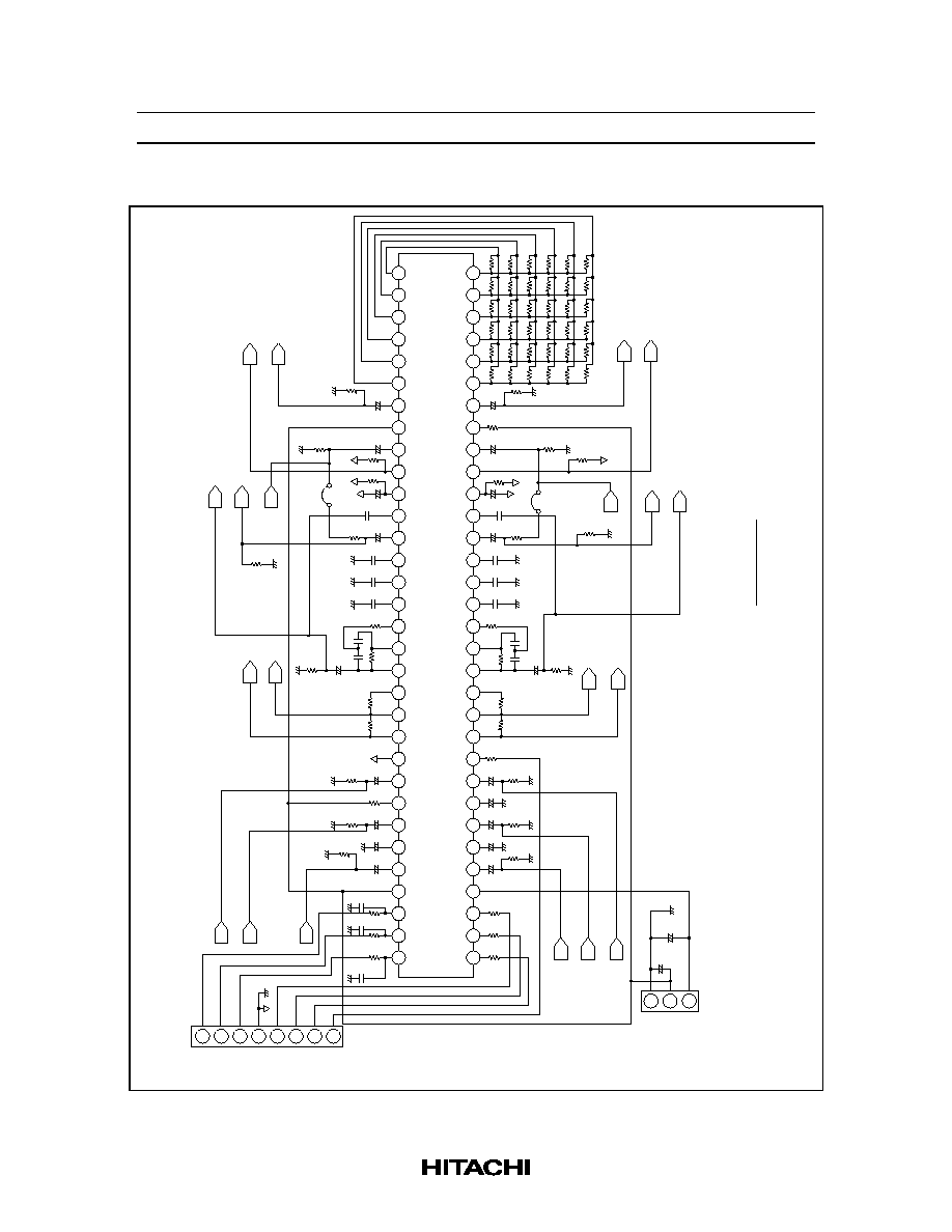
Block Diagram
DATA
CLK
STB
GND
(1)
VRI
(L)
CNT
(L)
RPI
(L)
BIAS
PBI
(L)
DGND
IA OUT
(L)
NRIN
(L)
PB OUT
(L)
REC
OUT(L)
LM
IN(L)
LM
OUT(L)
EQ
IN(L)
GND
(2)
EQ
OUT(L)
NN
NC
NM
HN
HC
HM
EQ-Controller
FM
fQ
f/Q
GH
GL
GP
EQ
OUT(R)
IREF
EQ
IN(R)
LM
OUT(R)
LM
IN(R)
REC
OUT(R)
PBOUT
(R)
Vref
(R)
NRIN
(R)
IA OUT
(R)
INJ
PBI
(R)
REF
RPI
(R)
CNT
(R)
VRI
(R)
V
CC
MPX
ON/OFF
C/B
NR
ON/OFF
BIAS
6BIT
DAC
SW
IA
IA
E VOL
6BIT
DAC
Shift
register
Latch
Decoder
Dolby B/C NR
RECT
REC
EQ
RECT
LMA
LMA
+
≠
+
≠
REC
EQ
M
P
X
64
63
61
60
59
58
57
56
55
54
53
52
51
50
49
48
47
46
45
44
43
42
41
40
39
38
37
36
35
34
33
45
6
7
8
9
10
11
12
13
14
15
16
17
18
19
20
21
22
23
24
25
26
27
28
29
30
31
32
3
2
1
62
Vref
(L)
M
P
X
Dolby B/C NR
E VOL
HA12155NT/HA12157NT
Rev.4, Jun. 1997, page 4 of 57
Absolute Maximum Ratings
Item
Symbol
Ratings
Unit
Supply voltage
V
CC
16
V
Power dissipation*1
Pd
770
mW
Operating temperature
Topr
≠30 to +75
∞C
Storage temperature
Tstg
≠55 to +125
∞C
Note:
1. Value at Ta
75∞C
Electrical Characteristics (Ta = 25∞C V
CC
= 14 V Dolby level 300 mVrms)
Item
Symbol
Min
Typ
Max
Unit
Test conditions
Notes
Quiescent current
I
Q
--
29.0
37.0
mA
no signal
Input amp gain
G
VIA
RPI
18.5
20.0
21.5
dB
Vin = 0 dB, f = 1 kHz
G
VIA
PBI
18.5
20.0
21.5
B-type NR Encode Boost B-ENC-2K
2.8
4.3
5.8
dB
Vin = ≠20 dB, f = 2 kHz
B-ENC-5K
1.7
3.2
4.7
Vin = ≠20 dB, f = 5 kHz
C-type NR Encode Boost C-ENC-1K(1)
3.9
5.9
7.9
dB
Vin = ≠20 dB, f = 1 kHz
C-ENC-1K(2)
18.1
19.6
21.6
Vin = ≠60 dB, f = 1 kHz
C-ENC-700
9.8
11.8
13.8
Vin = ≠30 dB, f = 700 Hz
Signal handling
Vomax
12.0
13.0
--
dB
f = 1 kHz, THD = 1%,
V
CC
= 12 V
*1
Signal to noise ratio
S/N
60.0
63.0
--
dB
Rg = 5.1 k
, CCIR/ARM
Total harmonic distortion
THD
--
0.08
0.3
%
Vin = 0 dB, f = 1 kHz
Crosstalk
C
T
(R
L)
--
≠85.0 ≠79.0 dB
Vin = 0 dB, f = 1 kHz
C
T
(RPI
PBI) --
≠80.0 ≠74.0
C
T
(VRI
RPI) --
≠77.0 ≠71.0
Control
Hi level
V
cH
3.5
--
5.3
V
MPX ON/OFF, NR
voltage
Lo level
V
cL
≠0.2
--
1.0
ON/OFF C-NR/B-NR
Serial data
Hi level
V
sH
3.5
--
5.3
V
CLK, DATA, STB
voltage
Lo level
V
sL
≠0.2
--
1.0
PB-out level
HA12155
Vout
500
580
670
mVrms Vin = 0 dB, f = 1 kHz
HA12157
665
775
900
PB-offset
Vofs
≠100 0.0
+100 mV
no signal
Channel balance
G
V
≠1.0
0.0
1.0
dB
Vin = 0 dB, f = 1 kHz
Volume gain
G
VVR (MAX)
17.5
19.3
21.5
dB
Vin = 100 mVrms, f =1 kHz
G
VVR (MIN)
--
--
≠55.0
Vin = 3 Vrms, f = 1 kHz

HA12155NT/HA12157NT
Rev.4, Jun. 1997, page 5 of 57
Electrical Characteristics (Ta = 25∞C V
CC
= 14 V Dolby level 300 mVrms) (cont)
Item
Symbol
Min
Typ
Max
Unit
Test conditions
Notes
Volume mute
G
VVR (MUT)
--
--
≠80.0 dB
Vin = 3 Vrms, f = 1 kHz
Max-input level to volume Vin max (VR)
11.0
12.6
--
dBs
f = 1 kHz, THD = 1%,
V
CC
= 12 V
Volume S/N
S/N (VR)
78.0
84.0
--
dB
Vin = 100 mVrms, f = 1
kHz, A-WTG
Volume THD
THD (VR)
--
0.04
0.3
%
Vin = 100 mVrms, f = 1
kHz
Equalizer gain
G
V EQ (500)
13.0
15.0
17.0
dB
Vin = 77.5 mVrms,
f = 500 Hz
G
V EQ (1K)
13.0
15.0
17.0
Vin = 77.5 mVrms,
f = 1 kHz
G
V EQ (5K)
14.5
16.5
18.5
Vin = 77.5 mVrms,
f = 5 kHz
G
V EQ (10K)
18.5
20.5
22.5
Vin = 77.5 mVrms,
f = 10 kHz
G
V EQ (20K)
29.5
32.0
34.5
Vin = 77.5 mVrms,
f = 20 kHz
Equalizer maximum input Vin max (EQ)
≠8.0
≠7.0
--
dBs
f = 1 kHz, THD = 1%,
V
CC
= 12 V
*1
Equalizer S/N
S/N (EQ)
57.0
62.0
--
dB
Rg = 5.1 k
, A-WTG
Equalizer THD
THD (EQ)
--
0.2
0.5
%
Vin = 77.5 mVrms,
f = 1 kHz
Equalizer offset
Vofs (EQ)
≠400 0.0
+400 mV
no signal
Level meter output
LM (0 dB)
2.60
2.85
3.10
V
Vin = 0 dB, f = 1 kHz
*2
LM (12 dB)
3.60
3.90
4.20
V
Vin = 12 dB, f = 1 kHz
Level meter output
LM (≠20 dB)1
0.80
1.10
1.40
V
Vin = ≠20 dB, f = 1 kHz
*2
LM (≠20 dB)2
2.55
3.0
3.15
V
Vin = ≠20 dB, f = 1 kHz,
≠20 dB range
Level meter offset
LMofs 1
--
150
300
mV
no signal
LMofs 2
--
200
350
no signal, ≠20 dB range
Notes: 1. HA12155 V
CC
= 9.5 V, HA12157 V
CC
= 12 V
2. 0 dB = PB-OUT level
HA12155NT/HA12157NT
Rev.4, Jun. 1997, page 6 of 57
Test Circuit
Mode
controller
AC VM 2
DC VM 2
AC VM 3
EQ
PB
RP
VR
SW4
µ
µ
µ
µ
µµ
µ
µ
µ
µ
µ
µ
µ
µ
µ
µ
µ
µ
µ
µ
µ
µ
µ
µ
µ
µ
Audio SG
AC VM 1
DC
Source 1
DC
Source 2
DC
Source 3
AC VM 4
Distortion
analyzer
Noise meter
R4
10 k
R5
10k
R6
10 k
R67
5.1 k
R66
5.1 k
C3
0.47
1
0.47
C33
C2
R29
18 k
C1
0.47
Degital
GND
SW8
TP3
T
P4
OFF
SW25
ON
R27
2.4 k
R26
5.6 k
R25
10 k
C30
2.2
C28
C29
2200p
2200p
R24
22 k
R23
560
C27
C26
C25
2200p
0.1
0.1
R21
20 k
C23
0.1
C24
2.2
C22
1
R20
100 k
R71
51 k
R22
7.5 k
C21
0.47
4.7
C20
R19
10 k
PB
REC
EQ
SW12
SW14
L
LM
EQ
REC
PB
ON
OFF
SW16
R1
22 k
R2
22 k
R3
22 k
SW18
SW19
SW20
OFF
ON
c
b
ON
SW21
SW23
S2
S3
S2
S3
L
ON
SW3
VR
RP
PB
EQ
OFF
SW1
R30
R31
R32
R33
R34
R35
R36
R37
R38
R39
R40
R41
R42
R43
R44
R45
R46
R47
R48
R49
R50
R51
R52
R53
R54
R55
R56
R57
R58
R59
R60
C4
C5
C6
C7
C8
0.47
1
R68
5.1 k
R69
5.1 k
R7
10 k
R9
2.4 k
R10
5.6 k
OFF
SW24
ON
TP2
TP1
SW7
R11
22 k
R13
560
C9
C10
2200 p
2200 p
C11
2.2
+
R12
10 k
C12
C
13
C14
2200p
0.1
0.1
C15 +
2.2
R14
20 k
R75
16 k
+
C16
0.1
C17
1
R16
100 k
C18
0.47
R17
24 k
C19
4.7
R18
10 k
100k
51 k
51 k
33 k
33 k
33 k
EQ
REC
PB
SW11
R
L
SW17
LM
EQ
REC
PB
SW13
NR
ON/OFF
C/B
MPX
ON/OFF
V
CC
VRI
(R)
CNT
(R)
RPI
(R)
REF
INJ
IA OUT
(R)
NRIN
(R)
V
(R)
PBOUT
(R)
SS1
(R)
SS2
(R)
CCR
(R)
HLS
DET(R)
REC
OUT(R)
LM
IN(R)
LM
DET(R)
LM
OUT(R)
EQ
IN(R)
IREF
PBI
(R)
EQ
OUT(R)
FM
FQ
F/Q
G
H
GL
GP
IA OUT
(L)
NRIN
(L)
V
(L)
PBOUT
(L)
SS1
(L)
SS2
(L)
CCR
(L)
HLS
DET(L)
REC
OUT(L)
LM
IN(L)
LM
DET(L)
LM
OUT(L)
PBI
(L)
EQ
IN(L)
EQ
OUT(L)
GND
(2)
NN
NC
NM
HN
HC
HM
64
63
62
61
60
59
58
57
56
55
54
53
52
51
50
49
48
47
46
45
44
43
42
41
40
39
38
37
36
35
34
33
1
2
34
5
6
7
89
10
11
12
13
14
15
16
17
18
19
20
21
22
23
24
25
26
27
28
30
31
32
DATA
CLK
S
TB
GND
(1)
VRI
(L)
CNT
(L)
RPI
(L)
BIAS
DGND
3
++
+
++
+
HA12155/7 NT (REC 1 CHIP)
DP-64S
R15
7.5 k
14 V
5
V
R
+
+
+
+
+
0.47
C32
100
Notes 1: Registor tolerance are ±1 %
2: Capacitor tolerance are ±1 %
3: Unit R: C:F
+
+
R28
10 k
+
REF
REF
R72
16 k
+
L
SW10
SW9
R70
51k
LLS
DET(L)
LLS
DET(R)
S2
S3
OFF
Oscilloscope
Noise meter with CCIR/ARM filter and A
≠
WTG filter
0.47
1
C60
10p
C61
10p
C62
10p
R8
1.2 k
29
SW22
SW15
R
+
R61
R62
R63
R64
R65
+
HA12155NT/HA12157NT
Rev.4, Jun. 1997, page 7 of 57
Example of Split Supply Circuit
0.47
µ
CN1
STB
CLK
DATA
DGND
C/B
MPX
ON/OFF
NR
ON/OFF
V
CC
2
(+5 V)
1
2
3
4
5
6
7
8
PBI (L)
RPI (L)
VRI (L)
R4
10 k
R5
10 k
R6
10 k
C3
++
1
µ
+
0.47
µ
C33
C2
R67
5.1 k
R66
5.1 k
R28
10 k
R29
18 k
C1
0.47
µ
Degital GND
R27
2.4 k
R26
5.6 k
R24
22 k
R23
560
C29
C28
C30
2.2
µ
+
+
R25
10 k
2200 p 2200 p
C27
2200 p
C26
C25
0.1
µ
0.1
µ
2.2
µ
C24
R21
20 k
C23
0.1
µ
++
C22
1
µ
R20
100 k
R71
51 k
+
C21
0.47
µ
+
C20
0.47
µ
R22
7.5 k
R19
10 k
EQOUT (L)
LMOUT (L)
PBOUT (L)
RECOUT (L)
EQIN (L)
R72
16 k
TP3
TP4
R1
22 k
R2
22 k
R3
22 k
0.47
µ
C4
+
C5
C6
C7
C8
++++
1
µ
0.47
µ
1
µ
0.47
µ
R68
5.1 k
R69
5.1 k
R7
10 k
R8
R9
2.4 k
R10
5.6 k
R11
22 k
R13
560
C9
C10
C11
2.2
µ
R12
10 k
+
2200 p
2200 p
2200 p
C12
C13
C14
C15
C16
C17
C18
C19
0.1
µ
0.1
µ
2.2
µ
+
R14
20 k
0.1
µ
1
µ
R16
100 k
R75
16 k
EQIN (R)
RECOUT (R)
PBOUT (R)
R70
51 k
R15
7.5 k
R18
10 k
+
4.7
µ
R30
R36
R42
R48
R54
R60
R31
R37
R43
R49
R55
R61
R32
R38
R44
R50
R56
R62
R33
R39
R45
R51
R57
R63
R34
R40
R46
R52
R58
R64
R35
R41
R47
R53
R59
R65
100 k
51 k
51 k
33 k
33 k
33 k
EQOUT (R)
LMOUT (R)
TP2
TP1
VRI (R)
RPI (R)
RBI (R)
CN2
C34
100
µ
+
+
C32
100
µ
GND
V
EE
V
CC
1
1
2
3
123456789
1
0
1
1
1
2
1
3
1
4
1
5
1
6
1
7
1
8
1
9
2
0
2
1
2
2
2
3
2
4
2
5
2
6
2
7
2
8
2
9
3
0
3
1
3
2
64
63
62
61
60
59
58
57
56
55
54
53
52
51
50
49
48
47
46
45
44
43
42
41
40
39
38
37
36
35
34
33
DATA
CLK
STB
GND
(1)
VRI
(L)
CNT
(L)
RPI
(L)
BIAS
PBI
(L)
DGND
IAOUT
(L)
NRIN
(L)
Vref
(L)
PBOUT
(L)
SS1
(L)
SS2
(L)
CCR
(L)
HLS
DET (L)
LLS
DET (L)
REC
OUT (L)
LM
IN (L)
LM
DET (L)
LM
OUT (L)
EQ
IN (L)
GND
(2)
EQ
OUT (L)
NN
NC
NM
HN
HC
HM
NR
ON/OFF
C/B
MPX
ON/OFF
V
CC
VRI
(R)
CNT
(R)
PRI
(R)
REF
PBI
(R)
I
NJ
IAOUT
(R)
NRIN
(R)
Vref
(R)
PBOUT
(R)
SS1
(R)
SS2
(R)
CCR
(R)
HLS
DET (R)
LLS
DET (R)
REC
OUT (R)
LM
IN (R)
LM
DET (R)
LM
OUT (R)
EQ
IN (R)
IREF
EQ
OUT (R)
F
M
F
Q
F
Q
G
H
G
L
G
P
HA12155/7 (REC 1 CHIP)
DP-64S
R17
+
+
0.47
µ
*1
Note 1:
The pin 10 can connect to V 1 through R8.
The value of external resistor R8 is obtained by using following equations.
3.6
V
≠
V
≠
0.7
INJ
E
E
R8 = (k )
CC
C62
10p
C61
10p
C60
10p
HA12155NT/HA12157NT
Rev.4, Jun. 1997, page 8 of 57
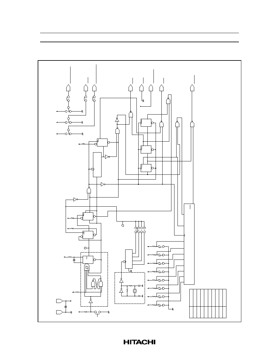
Mode Controller
GND
V (+5 V)
CC
C
100
µ
R
2
4
R
1
22 k
22 k
R
1 M
3
C
1
2.2
µ
Q
Q
SW9
X'tal OSC
N11 IC8
N12 IC8
R
22
X'tal
1 MHz
C
2
10 p
C
3
120 p
R
4
510
CLR
Q
A
Q
B
Q
C
Q
D
62.5 kHz
125 kHz
250 kHz
500 kHz
R
7
22 k
R
8
22 k
R
9
22 k
R
10
22 k
R
11
22 k
R
12
22 k
R
13
22 k
R
14
22 k
SW8
SW7
S
W6
SW5
S
W4
SW3
S
W2
SW1
AB
C
D
E
F
G
H
D IC4
7
CLK
CLK
INHIBIT
SHIFT
LOAD
Q
H
SW10
MCLK
D IC2
2
D IC2
1
TRIGGER
IC 1
CLR
TRIGGER
Q
Q
CLR
PR
D
Q
Q
CLR
PR
D
R
22 K
4
R
22 K
5
N13 IC8
N1 IC6
N5 IC8
Q
CLR
A
Q
B
Q
C
Q
D
D IC3
D IC9
Q
Q
CLR
PR
D
R
22 k
17
N3 IC6
N4 IC8
N6 IC6
D IC5
6
D IC5
5
D IC5
4
Q
Q
CLR
D
Q
Q
CLR
D
Q
Q
CLR
D
N7 IC6
N9 IC7
N10 IC7
DATA
CLK
V (+5 V)
GND
STB
MPX
∑
ON/OFF
C/B
NR
∑
ON/OFF
CC
N8 IC7
JP1
JP2
JP3
1
6
5
SW1
SW2
SW3
+
3
N2 IC8
9
D IC3
8
1M
1
4
8
2
3
Notes 1: HC type IC which operate eqaully is also applicable instead of IC1-IC9.
2: As for IC1-IC9, input pins which are not used should be pulled up with resistor of 22 k .
3: As for IC1-IC9, required to put 0.1 F-capacitor between near GND pin and Voltage source pin for bypass.
µ
Parts No.
IC1
IC2
IC3
IC4
IC5
IC6
IC7
IC8
IC9
Type
HD74HC221
HD74HC74
HD74HC393
HD74HC165
HD74HC175
HD74HC00
HD74HC00
HD74HC04
HD74HC74
4: Unit R : , C : F
+
HA12155NT/HA12157NT
Rev.4, Jun. 1997, page 9 of 57
Pin Description (V
CC
= 14 V, Ta = 25∞C, No signal, the value in the table show typical
value)
Pin No.
Terminal
DC
DP-64S
name
Zin
voltage
Equivalent circuit
Description
7
RPI
100 k
V
CC
/2
Recording input
58
9
PBI
Play back input
56
21
LM IN
HA12155
---75 k
Level meter input
44
HA12157
---100 k
24
EQ IN
100 k
Equalyzer input
41
5
VRI
100 k
V
CC
/2
Volume input
60
+0.7 V
4
V
CC
--
V
CC
--
Power supply
8
REF
--
V
CC
/2
--
Ripple filter
12
NR IN
--
V
CC
/2
NR processor input
53
15
SS 1
--
V
CC
/2
Spectral skewing amp
input
50
HA12155NT/HA12157NT
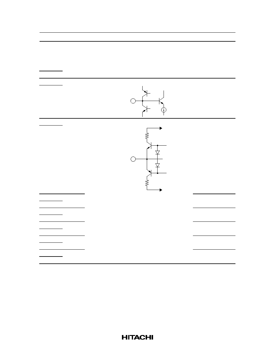
Rev.4, Jun. 1997, page 10 of 57
Pin Description (V
CC
= 14 V, Ta = 25∞C, No signal, the value in the table show typical
value) (cont)
Pin No.
Terminal
DC
DP-64S
name
Zin
voltage
Equivalent circuit
Description
17
CCR
--
V
CC
/2
Current controled
48
resistor output
11
IA OUT
--
V
CC
/2
Input amp output
54
V
GND
CC
13
VREF
Reference voltage
52
buffer output
14
PB OUT
Play back (Decode)
51
output
16
SS 2
Spectral skewing
49
amp. output
20
REC OUT
Recording (Encode)
45
output
26
EQ OUT
Equalyzer output
39
HA12155NT/HA12157NT
Rev.4, Jun. 1997, page 11 of 57
Pin Description (V
CC
= 14 V, Ta = 25∞C, No signal, the value in the table show typical
value) (cont)
Pin No.
Terminal
DC
DP-64S
name
Zin
voltage
Equivalent circuit
Description
18
HLS DET
--
2.3 V
Time constant pin for
47
rectifier
19
LLS DET
46
57
BIAS
--
0.28 V
GND
Dolby NR Reference
current input
25
IREF
--
1.2 V
EQ Reference current
input
27
FM
EQ Parameter current
28
fQ
input
29
f/Q
30
GH
31
GL
32
GP
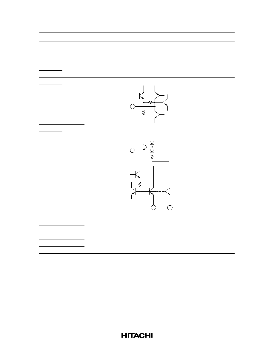
HA12155NT/HA12157NT
Rev.4, Jun. 1997, page 12 of 57
Pin Description (V
CC
= 14 V, Ta = 25∞C, No signal, the value in the table show typical
value) (cont)
Pin No.
Terminal
DC
DP-64S
name
Zin
voltage
Equivalent circuit
Description
33
HM
--
--
GND
EQ Parameter
selector
34
HC
35
HN
36
NM
37
NC
38
NN
6
CNT
5.2 k
V
CC
/2-
DAC output Volume
59
1.5 V to
V
CC
/2
V / 2
DAC
out
CC
control input
22
LMD
--
0.2 V
Time constant Pin for
43
LM OUT
GND
LMD
level meter
23
LM OUT
--
0.2 V
Level meter output
42
HA12155NT/HA12157NT
Rev.4, Jun. 1997, page 13 of 57
Pin Description (V
CC
= 14 V, Ta = 25∞C, No signal, the value in the table show typical
value) (cont)
Pin No.
Terminal
DC
DP-64S
name
Zin
voltage
Equivalent circuit
Description
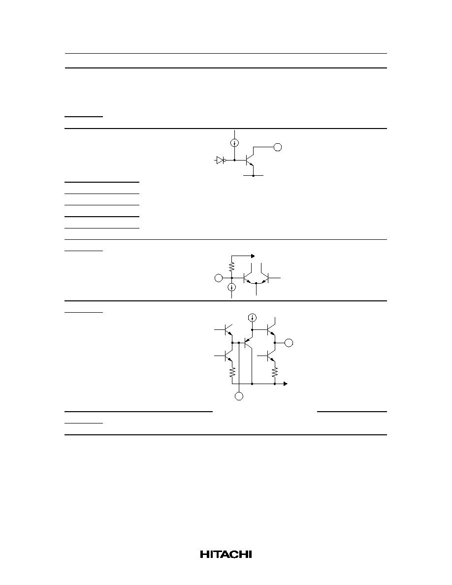
1
NR
ON/OFF
100 k
--
D - GND
GND
Mode control input
2
C/B
3
MPX
ON/OFF
62
STB
63
CLK
64
DATA
10
INJ
--
0.7 V
--
Injection current input
for I
2
L
55
D-GND
--
0.0 V
--
Digital (Logic) ground
40
GND
--
0.0 V
--
Ground
61
Application Note
Power Supply Range
HA12155NT/HA12157NT are designed to operate on either single supply or split supply.
The operating range of the supply voltage is shown in table 1.
Table 1
Supply Voltage
Type No.
Single supply
Split supply
HA12155NT
9.5 V to 16 V
±6 V to 8 V
HA12157NT
12 V to 16 V
±6 V to 8 V
The lower limit of supply voltage depends on the line output reference level.
HA12155NT/HA12157NT
Rev.4, Jun. 1997, page 14 of 57
The minimum value of the headroom margin is specified as 12 dB by Dolby Laboratories. HA12155 series
are provided with two line output level, which will permit an optimum headroom margin for power supply
conditions.
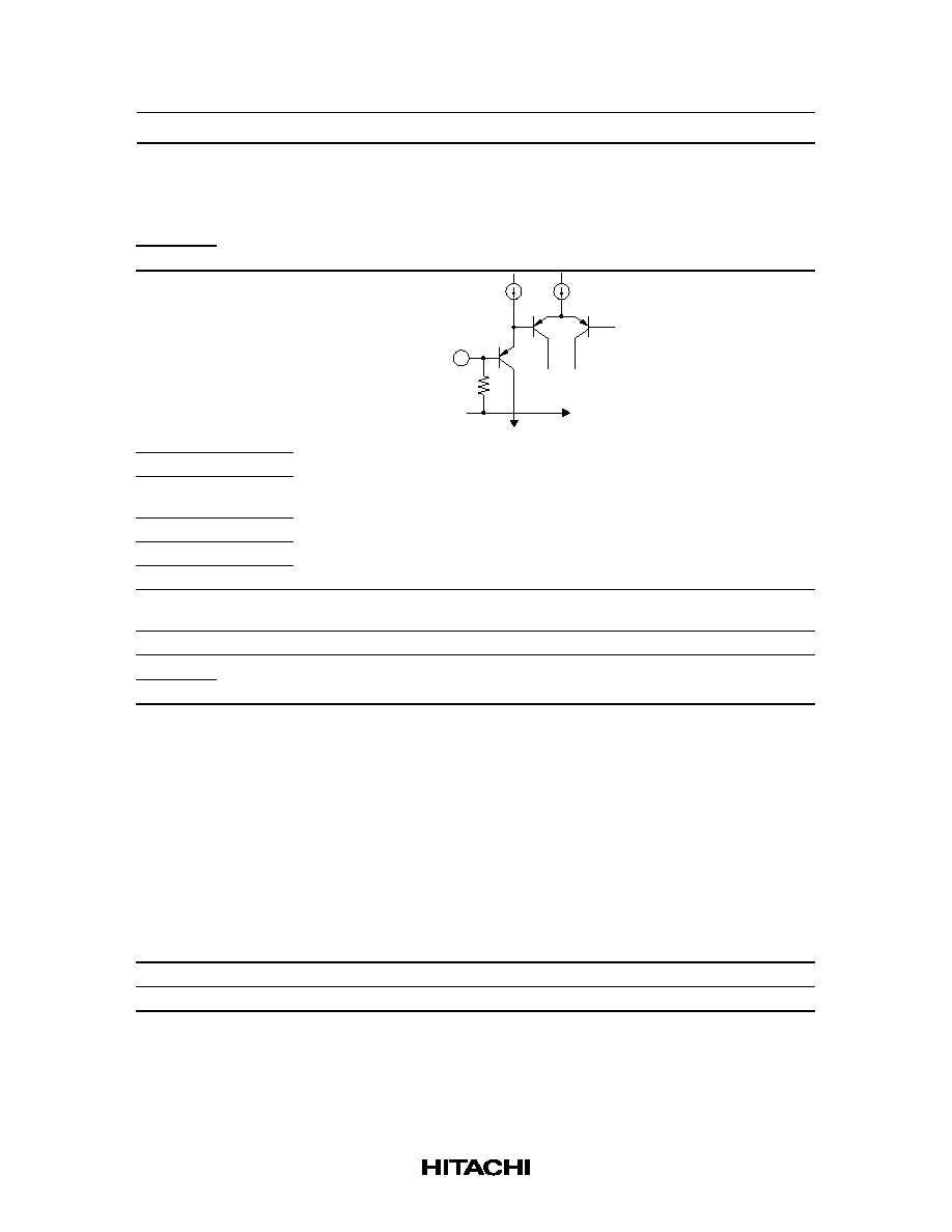
Reference Voltage
For the single supply operation these devices provide the reference voltage of half the supply voltage that is
the signal grounds. As the peculiarity of these devices, the capacitor for the ripple filter is very small about
1/100 compared with their usual value. The Reference voltage are provided for the left channel and the
right channel separately. The block diagram is shown as figure 1.
L channel
reference
R channel
reference
V
8
52
13
+
≠
≠
+
+
1 F
CC
µ
Figure 1 The Block Diagram of Reference Voltage Supply
Operating Mode Control
HA12155NT/HA12157NT provides fully electronic switching circuits. NR-ON/OFF, C/B, and MPX
ON/OFF switches are controlled by parallel data (DC voltage) and other switches are controlled by serial
data.
HA12155NT/HA12157NT
Rev.4, Jun. 1997, page 15 of 57
Table 2
Threshold Voltage (V
TH
)
Pin No.
Lo
Hi
Unit
1, 2, 3
≠0.2 to 1.0
3.5 to 5.3
V
62, 63, 64
≠0.2 to 1.0
3.5 to 5.3
V
Notes: 1. Voltages shown above are determined by internal circuits of LSI when take pin 55 (DGND pin) as
reference pin. On split supply use, same V
TH
can be offered by connecting DGND pin to GND
pin.
This means that it can be controlled directly by micro processor.
2. Each pins are on pulled down with 100 k
internal resistor.
Therefore, it will be low-level when each pins ar open.
3. Note on serial data inputting
(a)
The clock frequency on CLK must be less than 500 kHz.
(b)
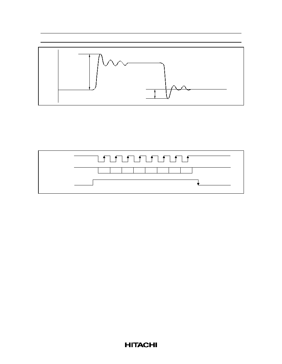
Over shoot level and under shoot level of input signal must be the value shown below.
(c)
The serial input pins (pins 62, 63, and 64) are extremely sensitive to undershoot, overshoot,
ringing, and noise. This can result in malfunctions due to problems with the wiring pattern.
We recommend attaching capacitors in parallel with the serial input pins to ameliorate this
problem.
Figure 2-b shows an example of this circuit appropriate when the clock frequency is 500
kHz. The value of the capacitor should be set in accordance with the clock frequency
actually used.
4. NR Mode Switching
In actual use, pop noises may accompany NR on/off switching in C mode. To avoid these
noises, use the following sequences to turn NR on and off.
From C mode NR off to C mode NR on:
(C mode, NR off)
(B mode, NR off)
(B mode, NR on)
(C mode, NR on).
From C mode NR on to C mode NR off:
(C mode, NR on)
(B mode, NR on)
(B mode, NR off)
(C mode, NR off).
Table 3
Switching Truth Table
Pin No.
Lo
Hi
1
NR-OFF
NR-ON
2
B-NR
C-NR
3
MPX-ON
MPX-OFF
Notes: 1. Low level will be offered when each pins are open.
2. Please refer to next term as for the serial data for formatting.
When connecting microcomputer or Logic-IC with HA12155NT/HA12157NT directly, there is
apprehension of rash-current under some transition timming of raising voltage or falling voltage at V
CC
ON/OFF.
For this countermeasure, connect 10 k
to 20 k
resistor with each pins. It is shown in test circuit.
HA12155NT/HA12157NT
Rev.4, Jun. 1997, page 16 of 57
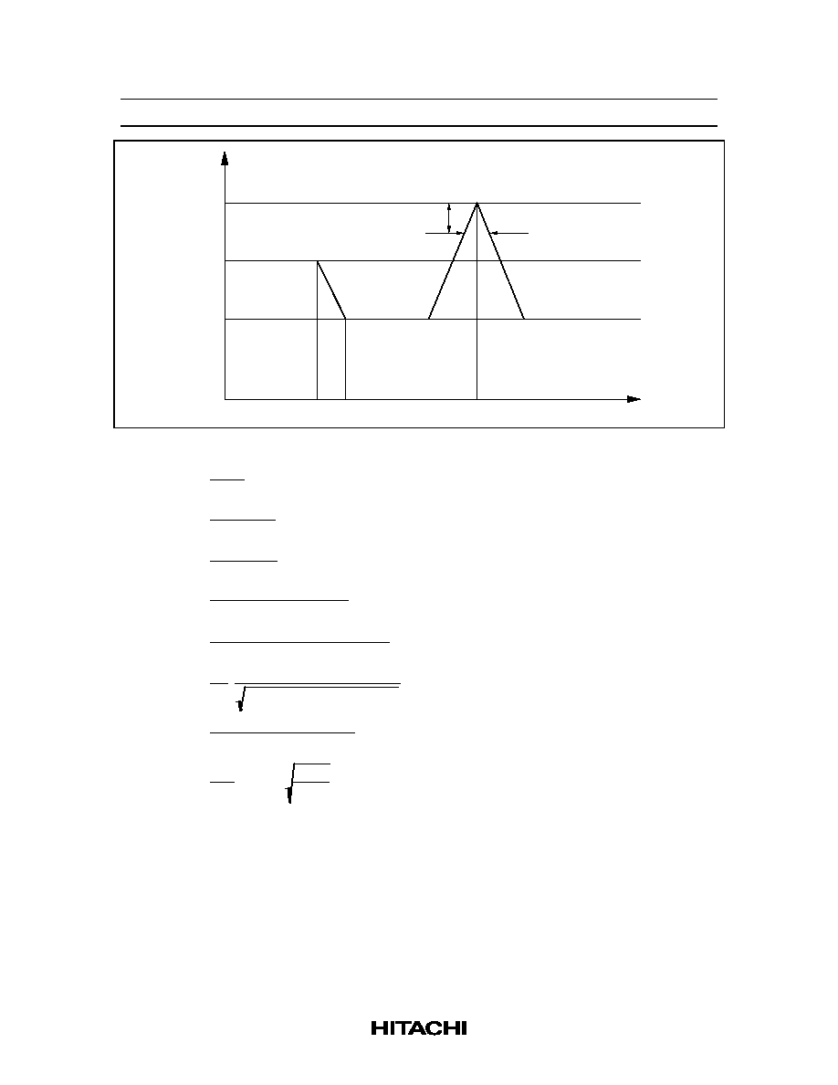
within ≠0.2 V
under 5.3 V
0
Figure 2 Input Level
Serial Data Formatting
8 bit shift register is employed. CLK and DATA are stored during STB being high and data is ratched
when STB goes high to low. The clock frequency on CLK must be less than 500 kHz.
0
1
2
3
4
5
6
7
latch of data
5 V
0 V
5 V
0 V
5 V
0 V
CLK
DATA
STB
Figure 3 Serial Data Timming Chart
HA12155NT/HA12157NT
Rev.4, Jun. 1997, page 17 of 57
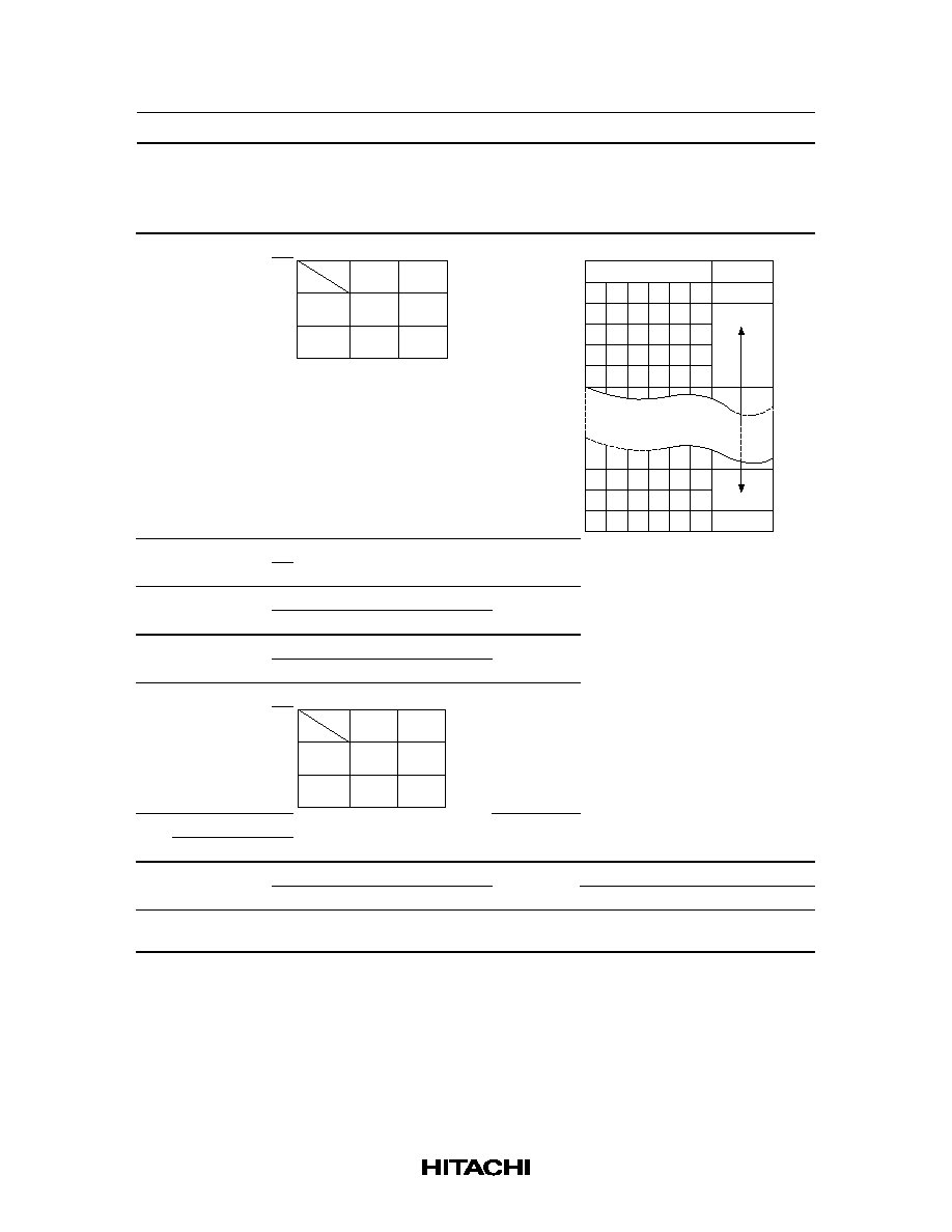
Table 4
Serial Data Formatting
Bit
No.
Control
register
Volume register
0
TAPE
H
DAC0
SELECT 1
L
TS1
TS2
H
H
L
L
TAPE
IV
TAPE
II
TAPE
I
TAPE
I
bit No.
5
4
3
2
1
0
L
L
L
L
L
L
L
L
L
L
L H
L
L
L L H L
L
L
L
L H H
H H H H L H
H H H H H L
H H H H H H
increase
gain
decrese
mute
1
TAPE
H
DAC1
*mute is implemented when all
SELECT 2
L
bits are high.
2
TAPE
H High (double) speed selection
DAC2
SPEED
L
Normal speed selection
3
METER
H Meter sensitivity 20 dB up
DAC3
SENSITIVITY
L
Meter sensitivity normal
4
INPUT
H
DAC4
SELECT 1
L
IS1
IS2
H
H
L
L
PB
I
RP
I
VR
I
VR
I
5
INPUT
H
DAC 5
SELECT 2
L
6
REC/PB
H PB mode selection
R/L SELECT H Rch register selection
L
REC mode selection
L
Lch register selection
7
REGISTER
SELECT
H Control register selection
REGISTER
SELECT
L
Volume register selection
Note:
TAPE I: Normal tape, TAPE II: Chrome tape, TAPE IV: Metal tape
HA12155NT/HA12157NT
Rev.4, Jun. 1997, page 18 of 57
Input Block Diagram and Level Diagram
≠3 dB
IA
OUT
NR
lN
MPX
Filter
RPI PBI
PB - OUT
NR
circuit
MPX ON
MPX OFF
≠ 3 dB
Input
Amp
Elect-
rical
VR
MA
VRI
43 mVrms
(≠25.2 dBs)
43 mVrms
(≠25.2 dBs)
426 mVrms
(≠5.2 dBs)
300 mVrms
(≠8.2 dBs)
HA12157
775 mVrms
(0 dBs)
HA12155
580 mVrms
(≠2.5 dBs)
47 mVrms
(≠24.3 dBs)
VRI
RPI PBI
IA
OUT
MPX
Filter
NR
lN
PB - OUT
HA12155
580 mVrms
(≠2.5 dBs)
HA12157
775 mVrms
(0 dBs)
NR
circuit
MA
Input
Amp
300 mVrms
(≠8.2 dBs)
30 mVrms
(≠28.2 dBs)
30 mVrms
(≠28.2 dBs)
Elect-
rical
VR
33 mVrms
(≠27.4 dBs)
NR circuit
The each level shown above is typical value when
offering Dolby level to test point pin (NR IN) with
the gain of electrical volume is under the condition
of max.
The each level shown above is typical value when
offering Dolby level to test point pin (IA OUT) with
the gain of electrical volume is under the condition
of max.
b) REC mode
a) PB mode
Figure 4 Input Block Diagram
HA12155NT/HA12157NT
Rev.4, Jun. 1997, page 19 of 57
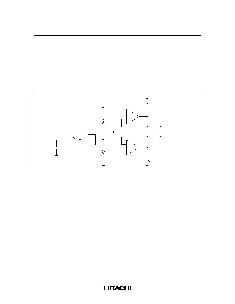
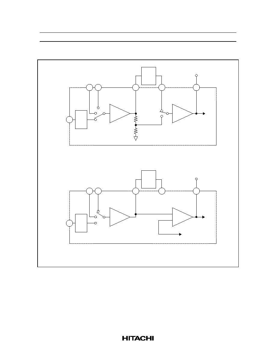
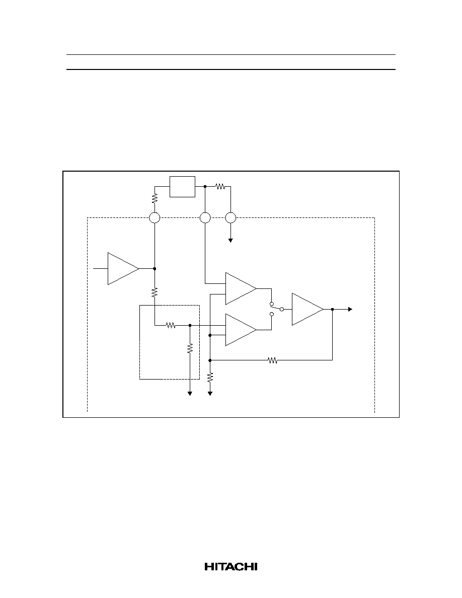
MPX ON/OFF Switch
MPX-OFF mode means that signal from input amp doesn't go through the MPX filter, but signal goes
through the SS circuit after being attenuated 3 dB by internal resistor. Refer to figure 5. For not cause any
level difference between MPX-ON mode and MPX-OFF mode, it is requested to use MPX-filter which has
definitely 3 dB attenuated. MPX-OFF mode offer totally flat frequency response and no bias-trap effect.
And when applying other usage except figure 5, take consideration to give bias voltage to NR-IN terminal
by resistor or so on because internal of NR-IN terminal hsa no bias resistor.
5.6 k
MPX
2.4 k
Vref
INPUT amp
MPX ON
MPX OFF
NR
PROCESSER
Vref
3 dB ATT.
IA OUT
NR IN
VREF
+
≠
+
≠
Figure 5 MPX ON/OFF Switch Block Diagram
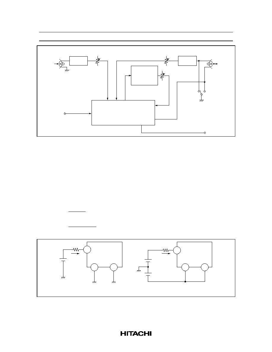
Application as for the Dubbing Cassette Deck
HA12155NT/HA12157NT series has unprocessor signal from recording out terminals during plyaback
mode. So, it is simply applied for dubbing cassette decks.
And HA12155NT/HA12157NT has three input terminal. So, it is applicable to switch the signal from PB-
EQ as shown below.
HA12155NT/HA12157NT
Rev.4, Jun. 1997, page 20 of 57
A deck
PB EQ
PB EQ
B deck
Compensation
of low
frequency
region
REC OUT
PBI
RPI
EQ IN
EQ OUT
VRI
REC IN
PB OUT
REC
PB
HA12155 / 7
Figure 6 Application for Dubbing Deck
Injector Current
HA12155NT/HA12157NT has logic circuit which is fabricated by I
2
L into IC. To operate this circuit, it is
required enough injector current. Injector current goes into from the INJ pin (pin 10) and external resistor
is required to connect to this pin for adequate current. The value of external resistor is obtained by using
following equations. And put them with ±10% tolerance value which is calculated. V
INJ
can allow to
connect to V
CC
shown below. Under the condition of high temperature, the mis-operation of logic is caused
by large injector current. Also, under the condition of low temperature, the stop of logic is caused by small
injector current. Therefore, pay attention to have good stability of V
INJ
.
R
INJ
=
V
INJ
≠ 0.7
3.6
[k
] ---- Single supply
R
INJ
=
V
INJ
+
V
EE
≠ 0.7
3.6
[k
] ---- Split supply
R
3.6 mA
V
HA12155 / 7
10
40
61
a) Single supply use
b) Split supply use
40
61
10
3.6 mA
HA12155 / 7
INJ
INJ
V
INJ
R
INJ
V
EE
Figure 7 Injector Current Application
HA12155NT/HA12157NT
Rev.4, Jun. 1997, page 21 of 57
Gain Control of Electronic Volume
HA12155NT/HA12157NT is designed in order to change the gain by 6 bit DAC fabricated into IC. To
reduce the click noise when changing volume gain instantaneously, required to connect the capacitor (CR
time constant) to CNT pin (pin 6,59). These terminals are also be used as output pin of DAC. Therefore,
by forcing voltage or current to these terminals, it is applicable to control volume gain directly. But,
voltage forced to these terminals must be from V
CC
/2 ≠2 V to V
CC
/2 (for split supply use, ≠2 V to 0 V) in this
case. In case of forcing the current these pins, voltage must be the value mentioned above even it is ±20%
distributed of internal resistor (5.2 k
) of CNT pin. And, these case, change of a gain depending on a
temperature gets large.
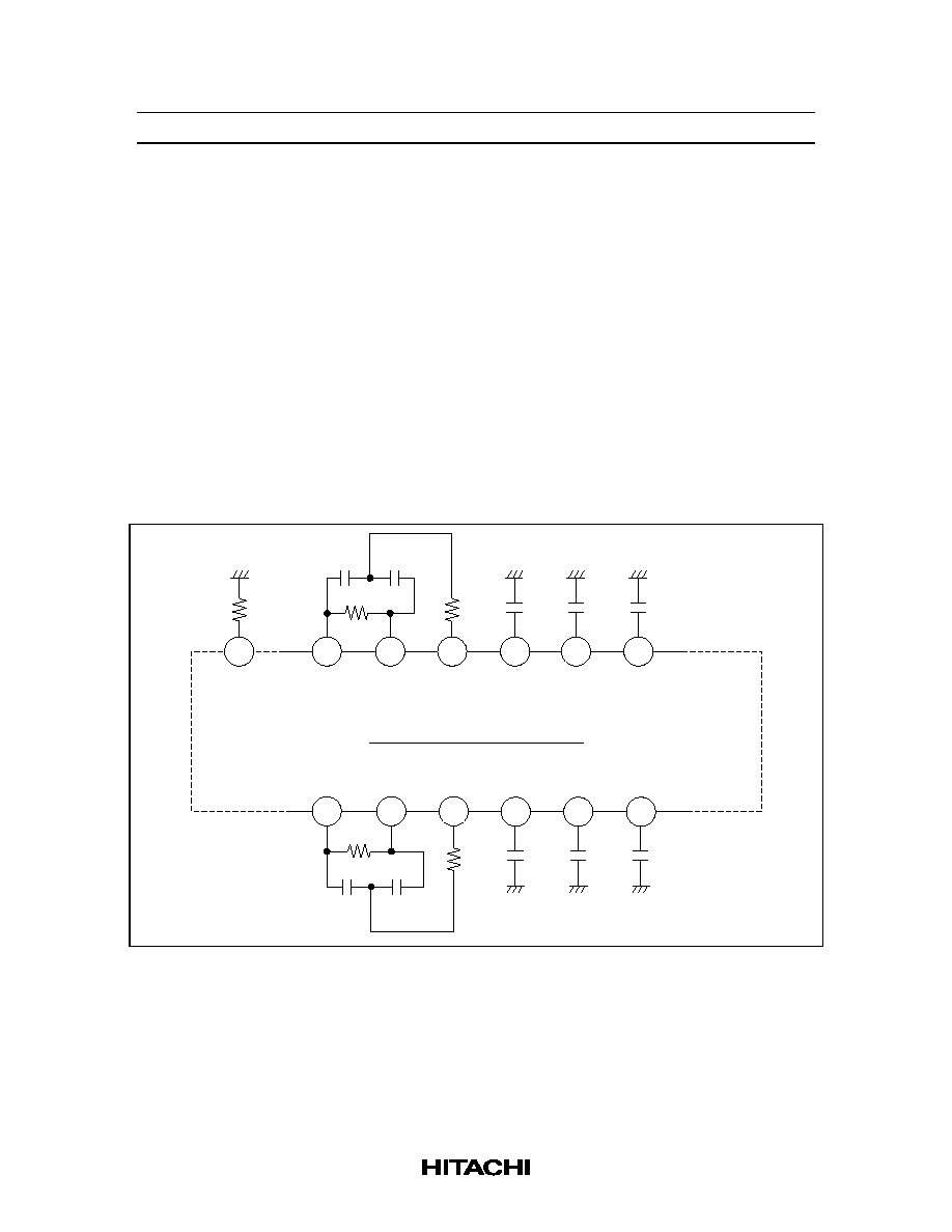
The Tolerances of External Components for Dolby NR-Block
For adequate Dolby NR tracking response, take external components shown below.
For smooth capacitors of C13, C14, C25 and C26, please employ a few object of the leak, though you can
be useful for an electrolytic capacitor.
C25
0.1
10%
C26
0.1
10%
C27
2200 p
5%
R23
560
2%
C29
2200 p
5%
C28
2200 p
5%
R24
22 k
2%
R29
18 k
2%
57
51
50
49
48
47
46
14
15
16
17
18
19
BIAS
PB OUT
(L)
SS1
(L)
SS2
(L)
CCR
(L)
HLS
DET(L)
LLS
DET(L)
PB OUT
(R)
SS1
(R)
SS2
(R)
CCR
(R)
HLS
DET(R)
LLS
DET(R)
R11
22 k
2%
C9
2200 p
5%
C10
2200 p
5%
R13
560
2%
C12
2200 p
5%
C13
0.1
10%
C14
0.1
10%
Unit R :
C : F
±
±
±
±
±
±
±
±
±
±
±
±
±
±
±
µ
µ
µ
µ
HA12155/7 (REC 1 Chip)
Figure 8 Tolerances of External Components
Level Meter
The coupling capacitor of LMIN pin (21 pin and 44 pin).
For these capacitors please employ a small object of the leak.
HA12155NT/HA12157NT
Rev.4, Jun. 1997, page 22 of 57
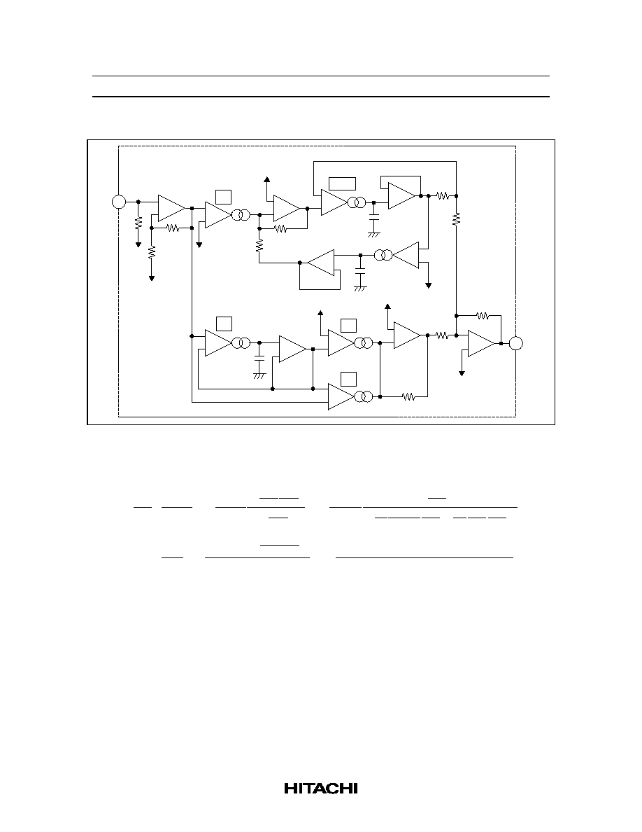
The Application of Equalizer Frequency Response
EQ
IN
R1
R2
R3
OP1
Gm1
OP2
Gm2
F / Q
OP5
R6
R7
R10
EQ
OUT
R9
R8
GH
GL
FM
R4
R5
Gm4
OP6
Gm3
OP3
Gm5
OP7
Gm6
OP4
C3
GP
C1
C2
+
_
+
_
+
_
+
_
+
_
+
_
+
_
+
_
_
+
_
+
_
+
_
+
_
+
Figure 9 REC Equalizer Block Diagram
Transfer Function:
Vout
Vin
=
R
2
+
R
3
R
2
Gm5
R
8
R
10
R
9
1
+
C3
Gm4
Gm6
Gm5
S
1
+
C3
Gm 4
S
+
Gm1
R
4
R
10
R
6
+
R
7
C2
Gm3
S
1
+
R
4
R
5
R7
R
6
+
R
7
C2
Gm3
S
+
R
4
R
5
C1
Gm 2
C2
Gm3
S
2
=
4.16
R
REF
R
GL
1
+
6.67
◊
10
-
10
R
FM
R
GH
R
GL
S
1
+
6.67
◊
10
-
10
R
FM
S
+
RGP
3.0
◊
10
-
10
R
FQ
S
1
+
4.5
◊
10
-
11
R
FQ
S
+
2.5
◊
10
-
20
R
FQ
R
F / Q
S
2
*R
REF
-----25 pin bias resistance
HA12155NT/HA12157NT
Rev.4, Jun. 1997, page 23 of 57
Gain
3dB
BW
f1
f2
f3
f
g1
g2
g3
Figure 10 REC Equalizer Frequency Response
gl
=
4.16
R
REF
6.67
◊
R
GP
+
R
GH
(
)
g 2
=
4.16
◊
R
GL
R
REF
g3
=
4.16
◊
R
GH
R
REF
f1
=
1
2
◊
6.67
◊
10
-
10
◊
R
FM
f 2
=
R
GL
2
◊
6.67
◊
10
-
10
◊
R
FM
◊
R
GH
f3
=
1
2
0.3
2.25
◊
10
-
21
◊
R
FQ
◊
R
F / Q
BW
=
1
4
◊
2.78
◊
10
-
10
◊
R
F / Q
Q
=
f3
BW
=
3.51
◊
R
F / Q
R
F / Q
HA12155NT/HA12157NT
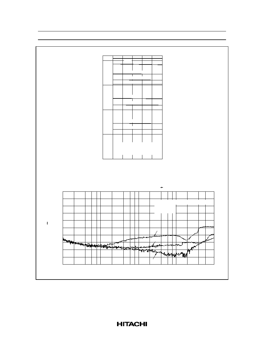
Rev.4, Jun. 1997, page 24 of 57
35
30
25
8
10
12
14
16
18
Quiescent current I (mA)
Supply voltage Vcc (V)
PB : PBI in (DAC Step 0)
LM : Normal
REC : VRI in (DAC Step 0)
LM : Normal
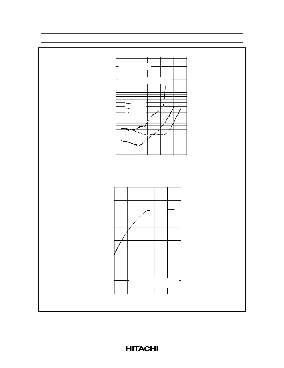
Quiescent Current vs. Supply Voltage
Q
REC ≠ C
REC ≠ B
REC ≠ OFF
PB ≠ C
PB ≠ B
PB ≠ OFF
HA12155NT/HA12157NT
Rev.4, Jun. 1997, page 25 of 57
12
10
8
6
4
2
0
100
200
500
1 k
2 k
5 k
10 k
20 k
50 k
100 k
Frequency (Hz)
NR≠B RPI in RECOUT out
Encode Boost (dB)
9 V
16 V
14 V
: Vin = ≠ 0 dB
: Vin = ≠ 10 dB
: Vin = ≠ 20 dB
: Vin = ≠ 30 dB
: Vin = ≠ 40 dB
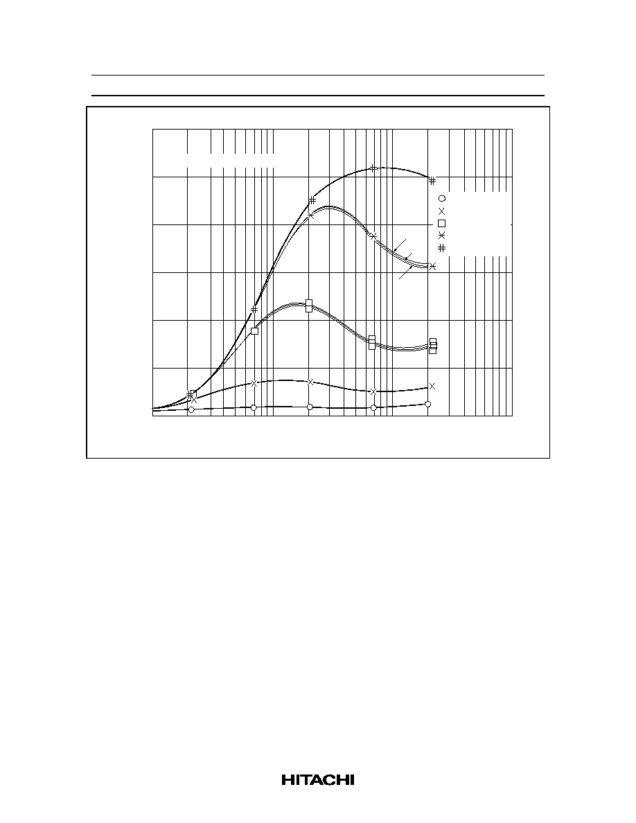
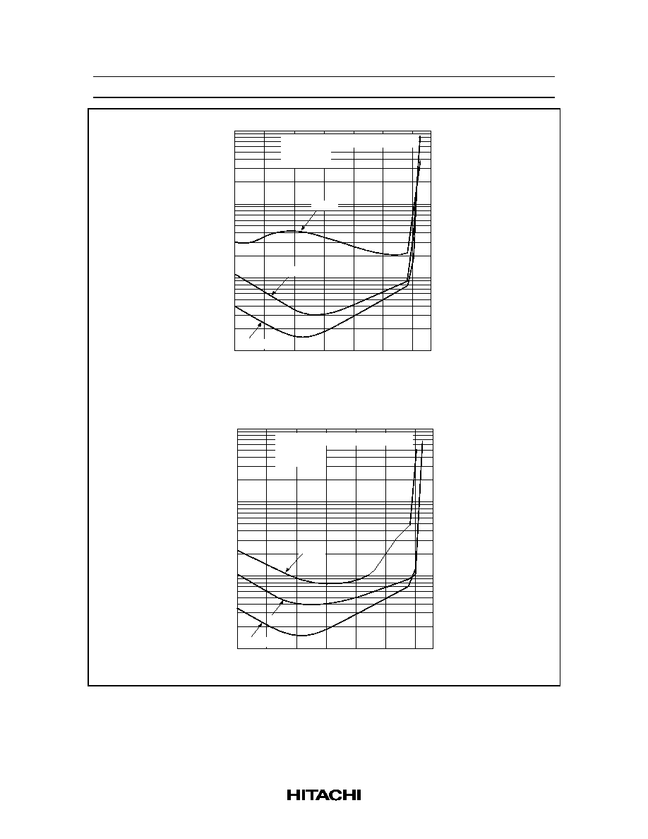
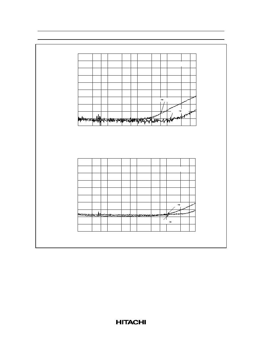
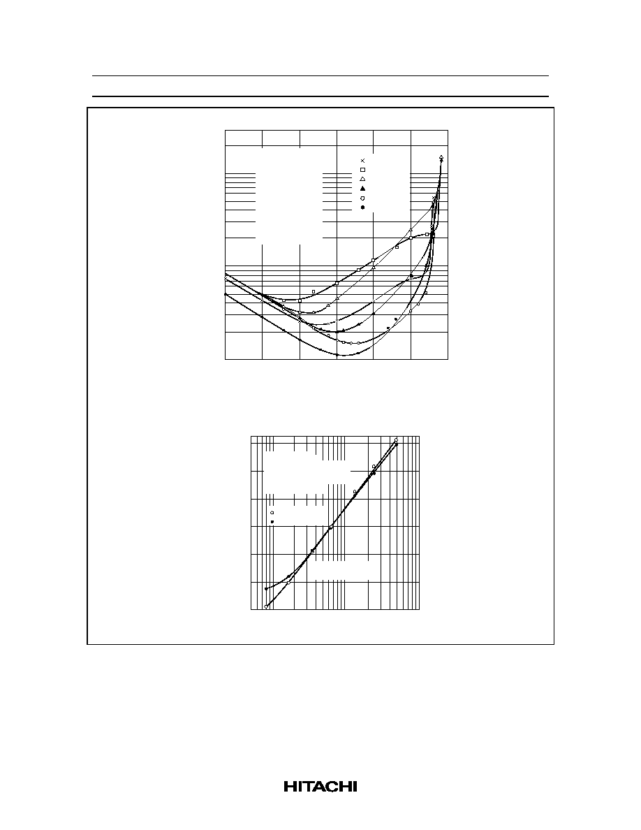
Encode Boost vs. Frequency (HA12155)
HA12155NT/HA12157NT
Rev.4, Jun. 1997, page 26 of 57
16 V
14 V
9 V
25
20
15
10
5
0
≠5
≠10
100
200
500
1 k
2 k
5 k
10 k
20 k
50 k
100 k
Frequency (Hz)
Encode Boost (dB)
NR-C RPI in RECOUT out
: Vin = 0 dB
: Vin = ≠ 20 dB
: Vin = ≠ 30 dB
: Vin = ≠ 40 dB
: Vin = ≠ 60 dB
Encode Boost vs. Frequency (HA12155)
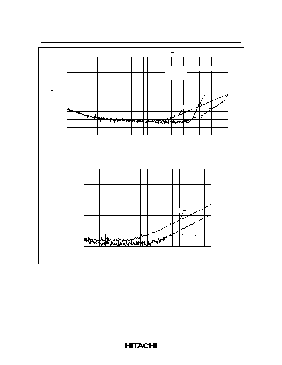
HA12155NT/HA12157NT
Rev.4, Jun. 1997, page 27 of 57
: Vin = 0 dB
: Vin = ≠ 10 dB
: Vin = ≠ 20 dB
: Vin = ≠ 30 dB
: Vin = ≠ 40 dB
12
10
8
6
4
2
0
100
200
500
1 k
2 k
5 k
10 k
20 k
50 k
100 k
Frequency (Hz)
Encode Boost (dB)
16 V
14 V
11 V
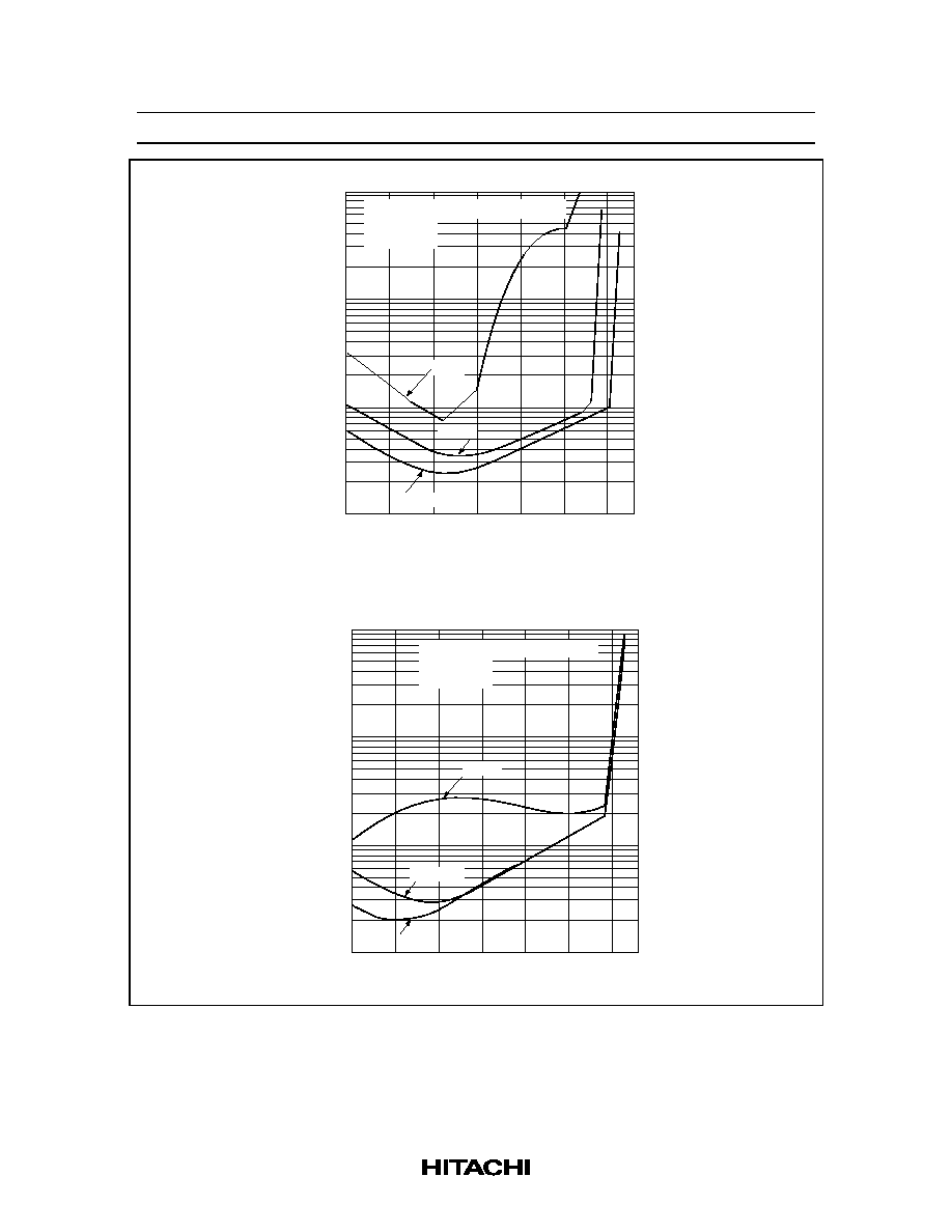
Encode Boost vs. Frequency (HA12157)
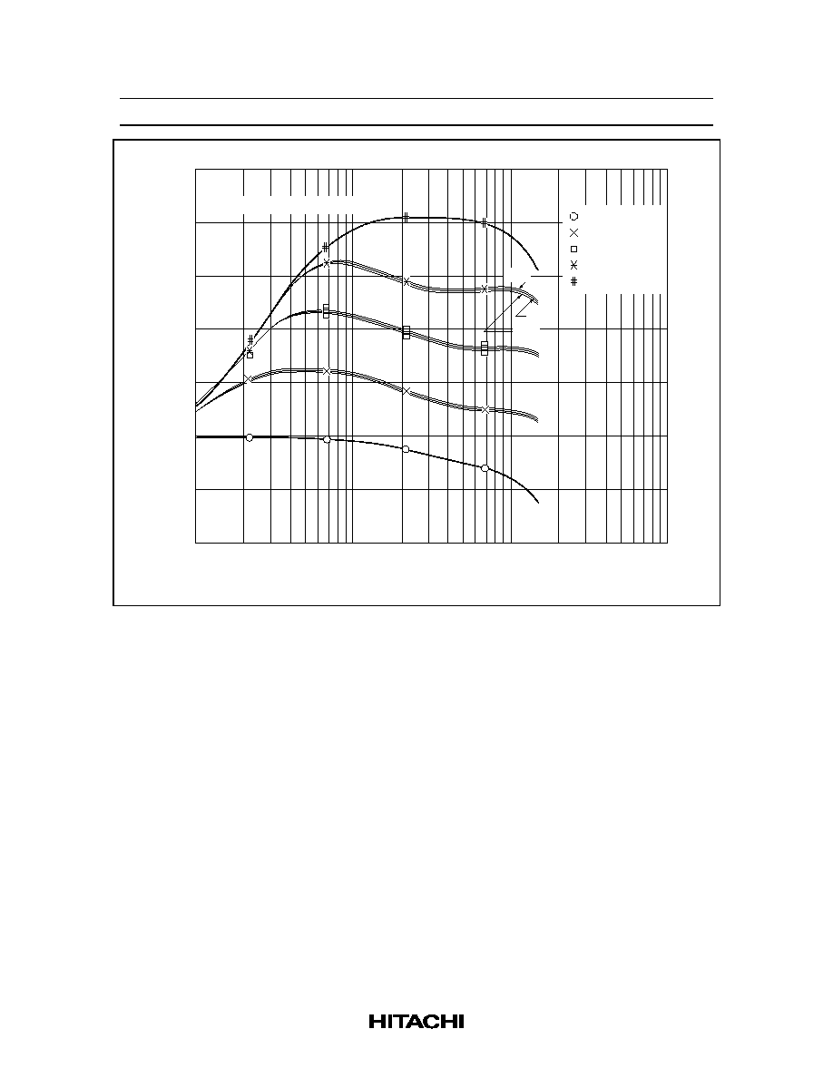
NR-B RPI in RECOUT out
HA12155NT/HA12157NT
Rev.4, Jun. 1997, page 28 of 57
Encode Boost vs. Frequency (HA12157)
25
20
15
10
5
0
≠ 5
≠ 10
100
200
500
1 k
2 k
5 k
10 k
20 k
50 k
100 k
Frequency (Hz)
Encode Boost (dB)
14 V
16 V
11 V
: Vin = ≠ 0 dB
: Vin = ≠ 20 dB
: Vin = ≠ 30 dB
: Vin = ≠ 40 dB
: Vin = ≠ 60 dB
NR-C RPI in RECOUT out

HA12155NT/HA12157NT
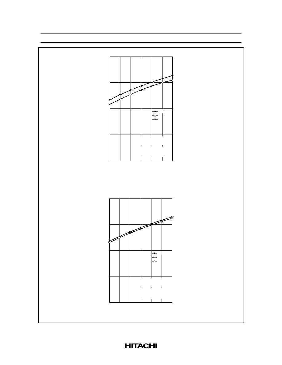
Rev.4, Jun. 1997, page 29 of 57
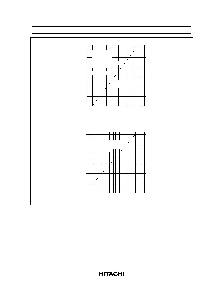
PB OUT
REC OUT
26
22
18
14
10
6
10
30
60 100
300
600
1 k
3 k
6 k 10 k
30 k 60 k 100 k
Frequency (Hz)
Output gain Gv (dB)
(NR ≠ OFF, RPI) Vcc = 14 V
REC mode
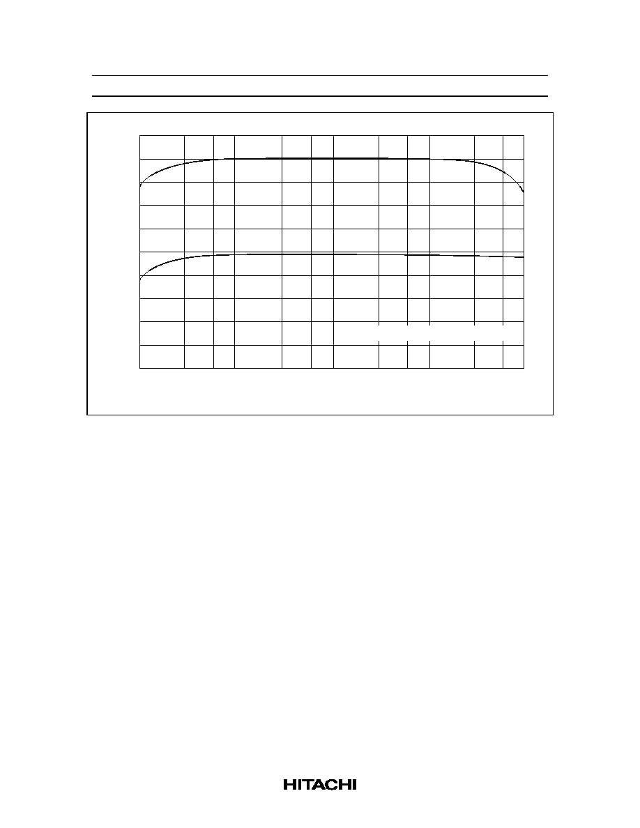
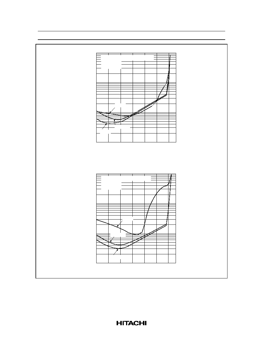
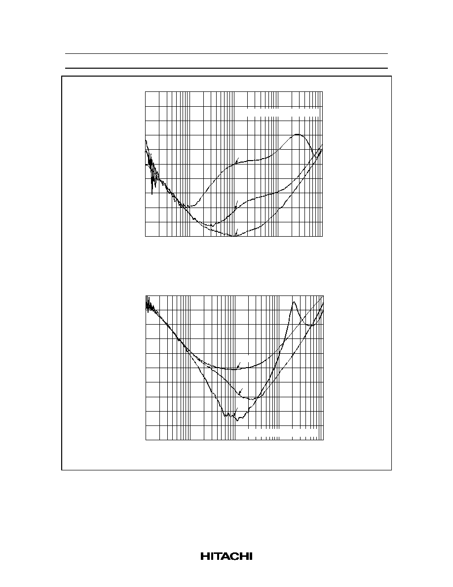
Output Gain vs. Frequency (HA12155)
HA12155NT/HA12157NT
Rev.4, Jun. 1997, page 30 of 57
PB OUT
REC OUT
28
24
20
16
12
8
10
30
60 100
300
600 1 k
3 k
6 k 10 k
30 k
60 k 100 k
Frequency (Hz)
Output gain Gv (dB)
PB mode (NR ≠ OFF, RPI) Vcc = 14 V
Output Gain vs. Frequency (HA12155)
HA12155NT/HA12157NT
Rev.4, Jun. 1997, page 31 of 57
PB OUT
REC OUT
10
30
60
100
300
600 1 k
3 k
6 k 10 k
30 k
60 k 100 k
Frequency (Hz)
28
24
20
16
12
8
Output gain Gv (dB)
(NR ≠ OFF, RPI) Vcc = 14 V
REC mode
Output Gain vs. Frequency (HA12157)
HA12155NT/HA12157NT
Rev.4, Jun. 1997, page 32 of 57
PB OUT
REC OUT
10
30
60 100
300
600 1 k
3 k
6 k 10 k
30 k
60 k 100 k
30
26
22
18
14
10
Frequency (Hz)
Out put gain Gv (dB)
Output Gain vs. Frequency (HA12157)
PB mode (NR ≠ OFF, PBI) Vcc = 14 V
HA12155NT/HA12157NT
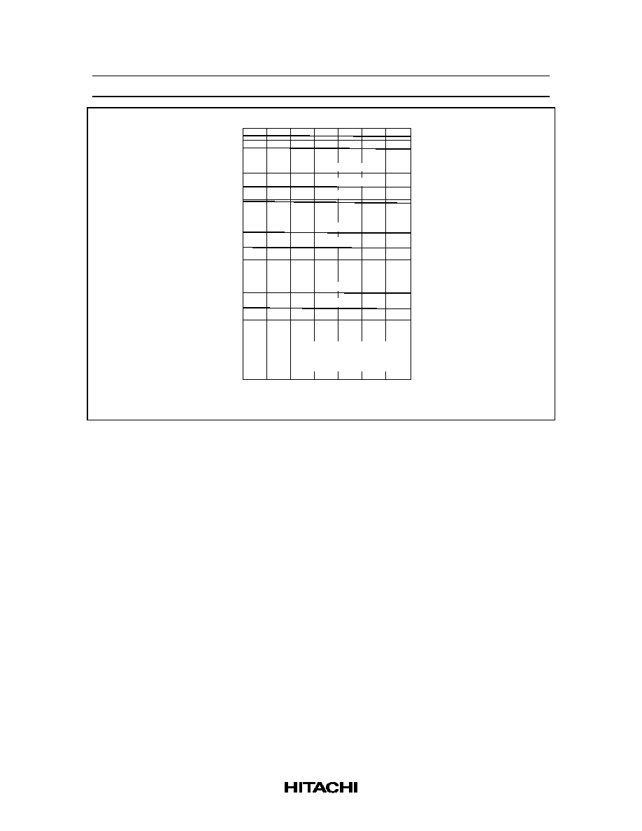
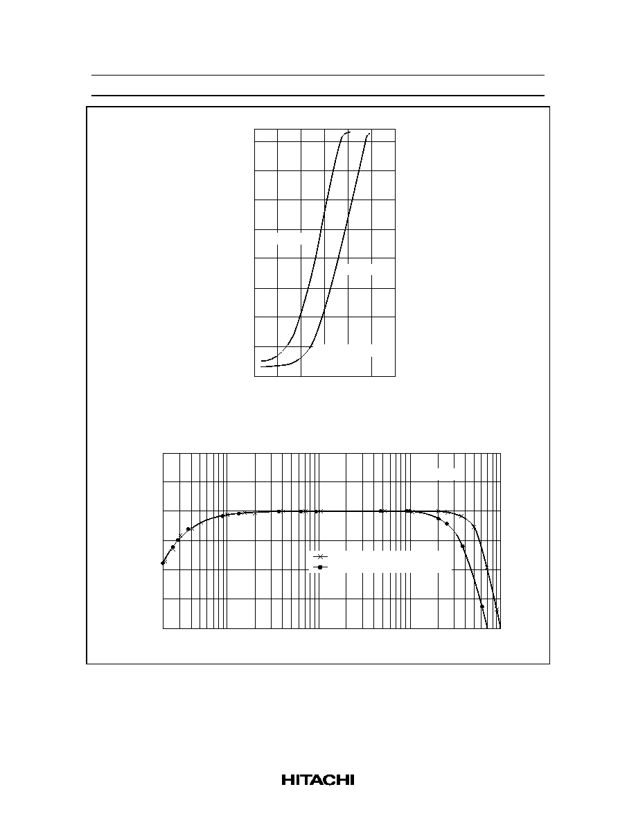
Rev.4, Jun. 1997, page 33 of 57
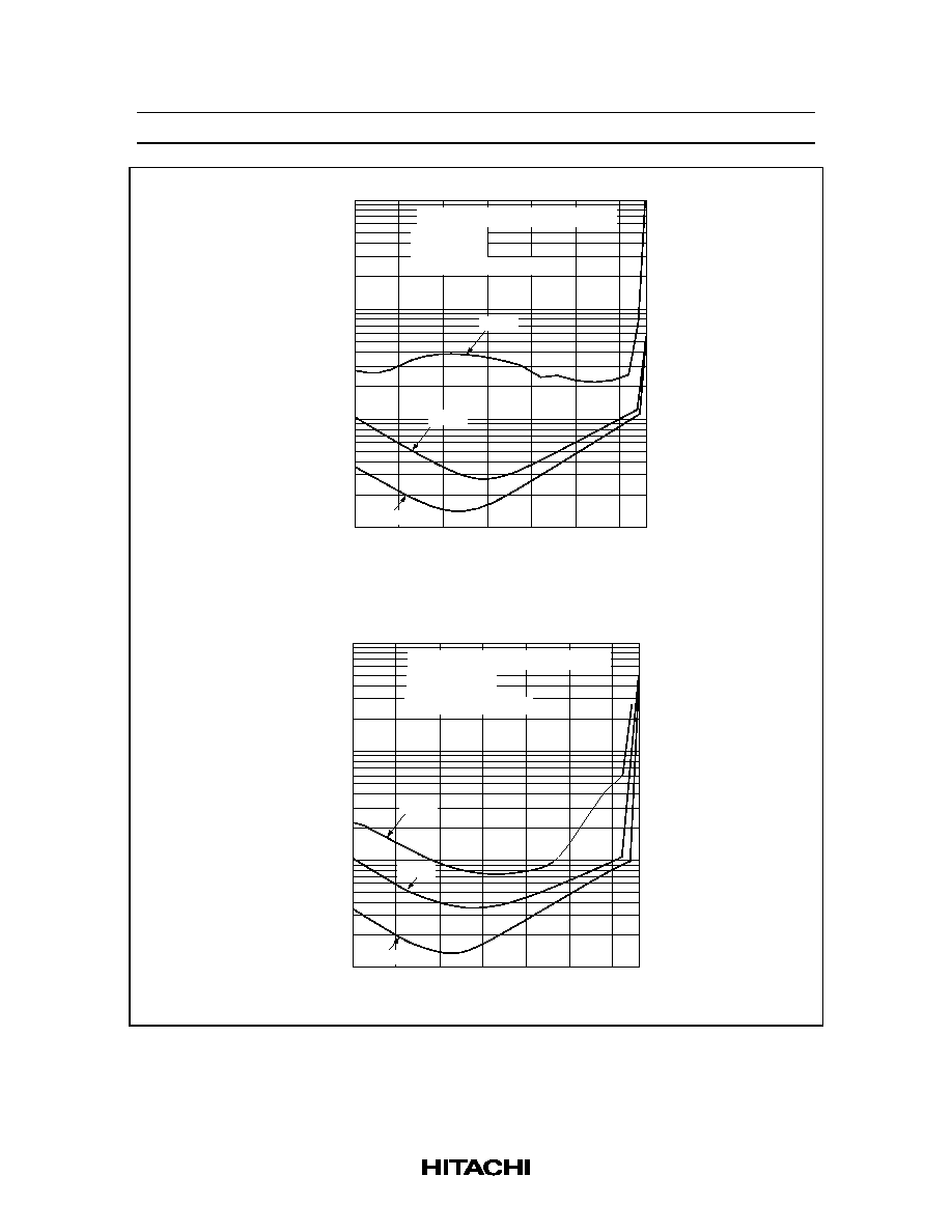
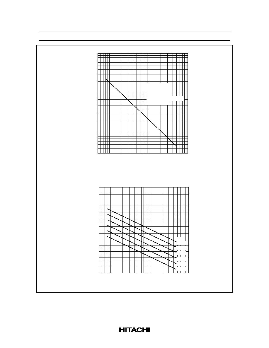
NR-C
NR-B
NR-OFF
≠15
≠10
≠5
0
5
10
15
0.01
0.03
0.1
0.3
1.0
3.0
10
Output level Vout (dB)
Total harmonic distortin T.H.D. (%)
CC
RPI in RECOUT out REC mode
f = 100 Hz
V = 14 V
0 dB = 300 mVrms
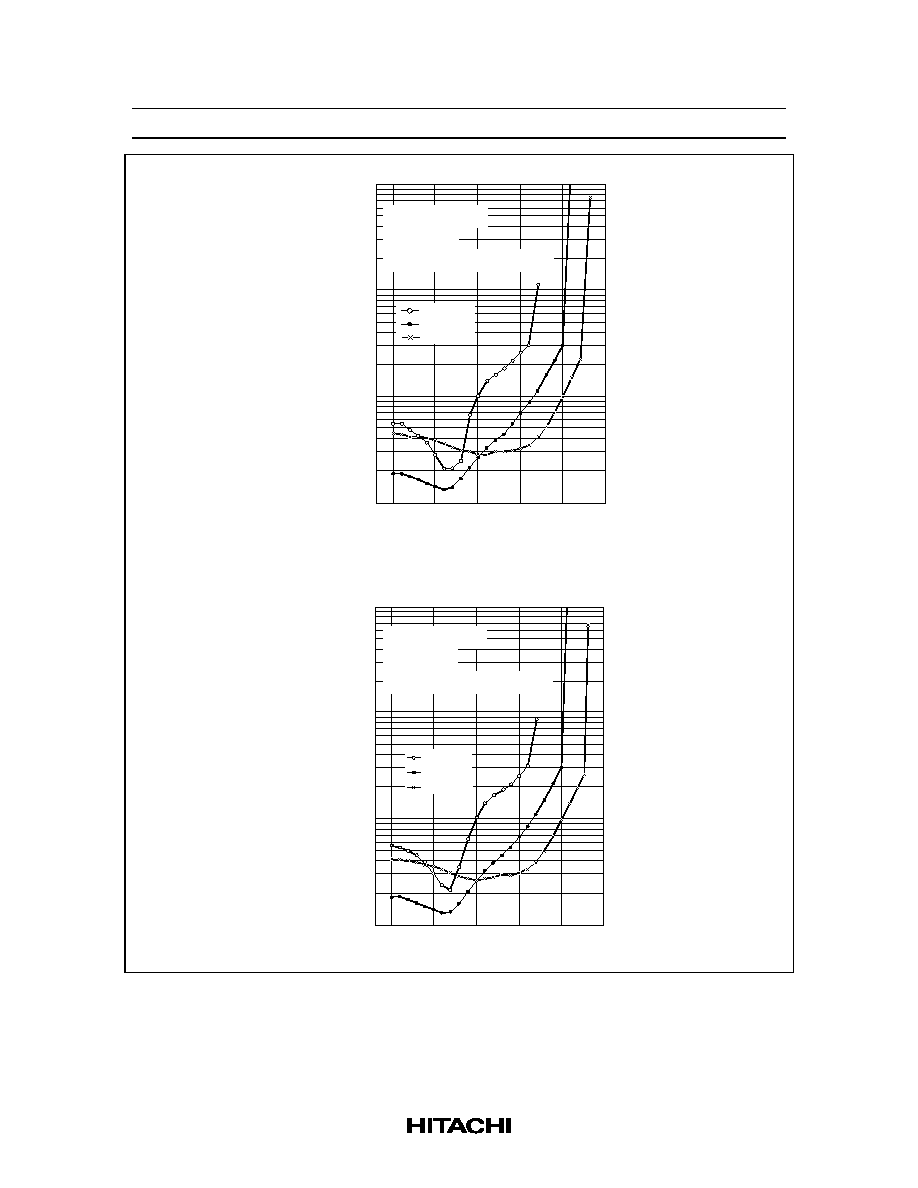
Total Harmonic Distortion vs. Output Level (HA12155)
NR-C
NR-B
NR-OFF
≠15
≠10
≠5
0
5
10
15
0.01
0.03
0.1
0.3
1.0
3.0
10
Output level Vout (dB)
Total harmonic distortion T.H.D. (%)
CC
RPI in RECOUT out REC mode
f = 1 kHz
V = 14 V
0 dB = 300 mVrms
Total Harmonic Distortion vs. Output Level (HA12155)
HA12155NT/HA12157NT
Rev.4, Jun. 1997, page 34 of 57
NR-C
NR-B
NR-OFF
≠15
0.01
0.03
0.1
0.3
1.0
3.0
10
Total harmonic distortion T.H.D. (%)
Total Harmonic Distortion vs. Output Level (HA12155)
≠10
≠5
0
5
10
15
Output level Vout (dB)
RPI in RECOUT out REC mode
f = 10 kHz
V = 14 V
0 dB = 300 mVrms
CC
NR-C
NR-B
NR-OFF
≠15
≠10
≠5
0
5
10
15
0.01
0.03
0.1
0.3
1.0
3.0
10
Output level Vout (dB)
Total harmonic distortion T.H.D. (%)
CC
PBI in PBOUT out PB mode
f = 100 Hz
V = 14 V
0 dB = 580 mVrms
Total Harmonic Distortion vs. Output Level (HA12155)
HA12155NT/HA12157NT
Rev.4, Jun. 1997, page 35 of 57
NR-C
NR-B
NR-OFF
≠15
0.01
0.03
0.1
0.3
1.0
3.0
10
Total harmonic distortion T.H.D. (%)
Total Harmonic Distortion vs. Output Level (HA12155)
PBI in PBOUT out PB mode
f = 1 kHz
V = 14 V
0 dB = 580 mVrms
CC
≠10
≠5
0
5
10
15
Output level Vout (dB)
NR-C
NR-B
NR-OFF
≠15
0.01
0.03
0.1
0.3
1.0
3.0
10
Total harmonic distortion T.H.D. (%)
Total Harmonic Distortion vs. Output Level (HA12155)
PBI in PBOUT out PB mode
f = 10 kHz
V = 14 V
0 dB = 580 mVrms
CC
≠10
≠5
0
5
10
15
Output level Vout (dB)
HA12155NT/HA12157NT
Rev.4, Jun. 1997, page 36 of 57
NR-C
NR-B
NR-OFF
≠15
0.01
0.03
0.1
0.3
1.0
3.0
10
Total harmonic distortion T.H.D. (%)
Total Harmonic Distortion vs. Output Level (HA12157)
RPI in RECOUT out REC mode
f = 100 Hz
V = 14 V
CC
≠10
≠5
0
5
10
15
Output level Vout (dB)
NR-C
NR-B
NR-OFF
≠15
0.01
0.03
0.1
0.3
1.0
3.0
10
Total harmonic distortion T.H.D. (%)
Total Harmonic Distortion vs. Output Level (HA12157)
RPI in RECOUT out REC mode
f = 1 kHz
V = 14 V
CC
≠10
≠5
0
5
10
15
Output level Vout (dB)
HA12155NT/HA12157NT
Rev.4, Jun. 1997, page 37 of 57
NR-C
NR-B
NR-OFF
≠15
0.01
0.03
0.1
0.3
1.0
3.0
10
Total harmonic distortion T.H.D. (%)
Total Harmonic Distortion vs. Output Level (HA12157)
RPI in RECOUT out REC mode
f = 10 kHz
V = 14 V
CC
≠10
≠5
0
5
10
15
Output level Vout (dB)
NR-C
NR-B
NR-OFF
≠15
0.01
0.03
0.1
0.3
1.0
3.0
10
Total harmonic distortion T.H.D. (%)
Total Harmonic Distortion vs. Output Level (HA12157)
RBI in RBOUT out PB mode
f = 100 Hz
V = 14 V
CC
≠10
≠5
0
5
10
15
Output level Vout (dB)
HA12155NT/HA12157NT
Rev.4, Jun. 1997, page 38 of 57
NR-C
NR-B
NR-OFF
≠15
0.01
0.03
0.1
0.3
1.0
3.0
10
Total harmonic distortion T.H.D. (%)
Total Harmonic Distortion vs. Output Level (HA12157)
PBI in PBOUT out REC mode
f = 10 kHz
V = 14 V
CC
≠10
≠5
0
5
10
15
Output level Vout (dB)
NR-C
NR-B
NR-OFF
≠15
0.01
0.03
0.1
0.3
1.0
3.0
10
Total harmonic distortion T.H.D. (%)
Total Harmonic Distortion vs. Output Level (HA12157)
PBI in PBOUT out PB mode
f = 10 kHz
V = 14 V
CC
≠10
≠5
0
5
10
15
Output level Vout (dB)
HA12155NT/HA12157NT
Rev.4, Jun. 1997, page 39 of 57
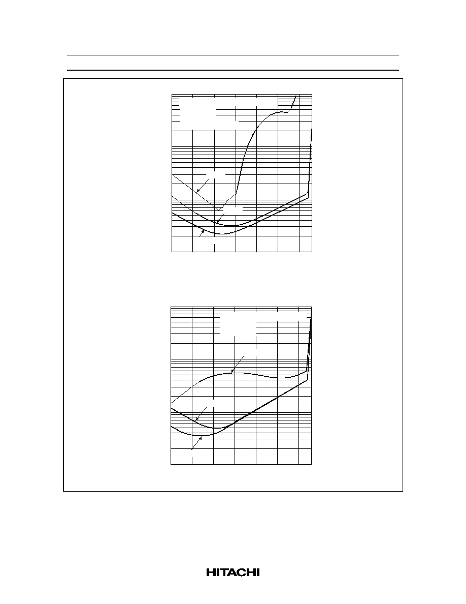
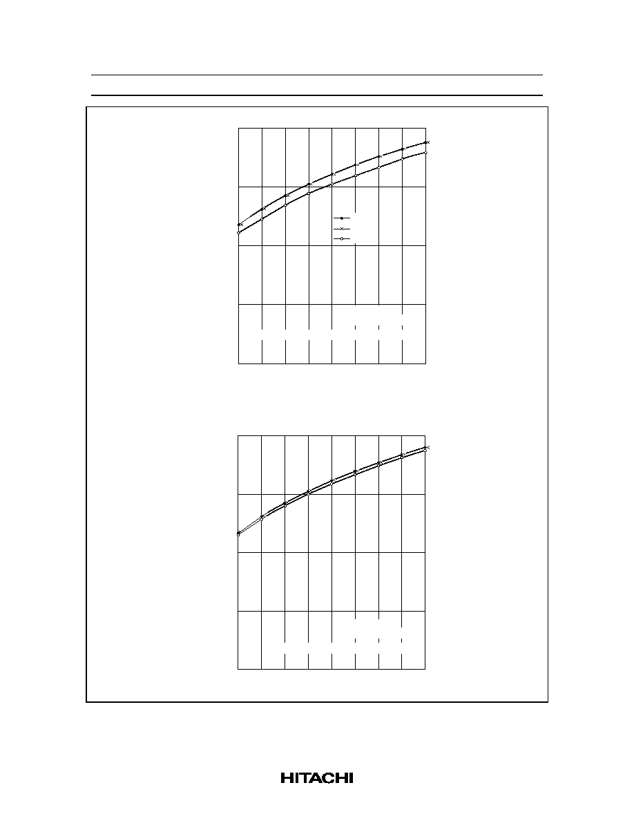
Max. Output Level vs. Supply Voltage (HA12155)
Supply voltage V (V)
CC
Max. output level Vo max (dB)
T.H.D. = 1%
0 dB = 300 mVrms
f = 1 kHz REC mode RPI in RECOUT out
OFF
B
C
8
9
10
11
12
13
14
15
16
0
5
10
15
20
Max. Output Level vs. Supply Voltage (HA12155)
Supply voltage V (V)
CC
Max. output level Vo max (dB)
T.H.D. = 1%
0 dB = 580 mVrms
f = 1 kHz PB mode PBI in PBOUT out
8
9
10
11
12
13
14
15
16
0
5
10
15
20
HA12155NT/HA12157NT
Rev.4, Jun. 1997, page 40 of 57
Max. Output Level vs. Supply Voltage (HA12157)
Max. output level Vo max (dB)
Supply voltage V (V)
CC
f = 1 kHz REC mode
RPI in RECOUT out
9
10
11
12
13
15
16
0
10
15
20
5
T.H.D. = 1%
0 dB = 300 mVrms
B
C
OFF
Max. Output Level vs. Supply Voltage (HA12157)
Max. output level Vo max (dB)
Supply voltage V (V)
CC
f = 1 kHz PB mode
PBI in PBOUT out
10
11
12
13
14
15
16
0
10
15
20
5
T.H.D. = 1%
0 dB = 775 mVrms
B
C
OFF
HA12155NT/HA12157NT
Rev.4, Jun. 1997, page 41 of 57
PB-C
PB-B
REC-OFF RPI
REC-OFF VRI
PB-OFF
REC-B RPI
REC-B VRI
REC-C RPI
REC-C VRI
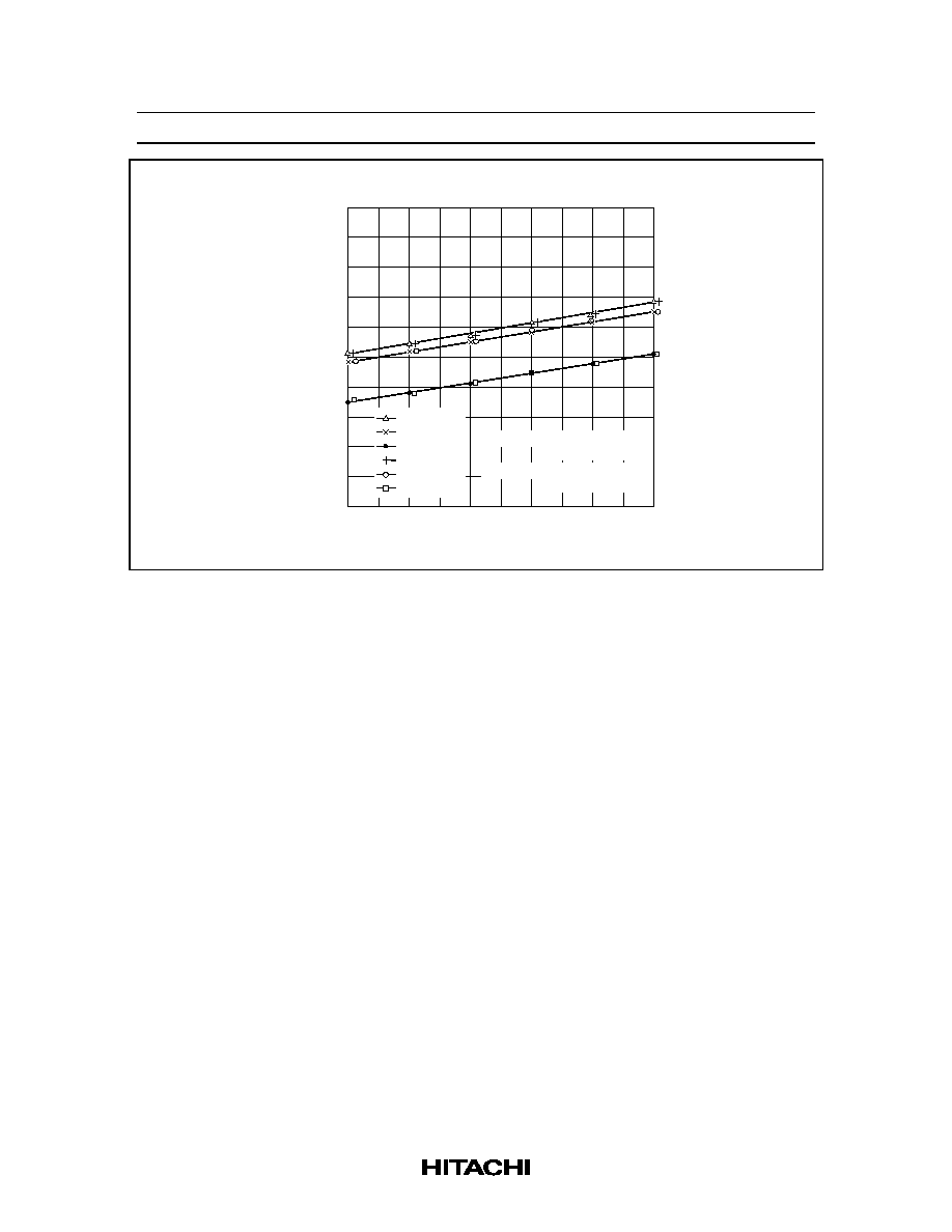
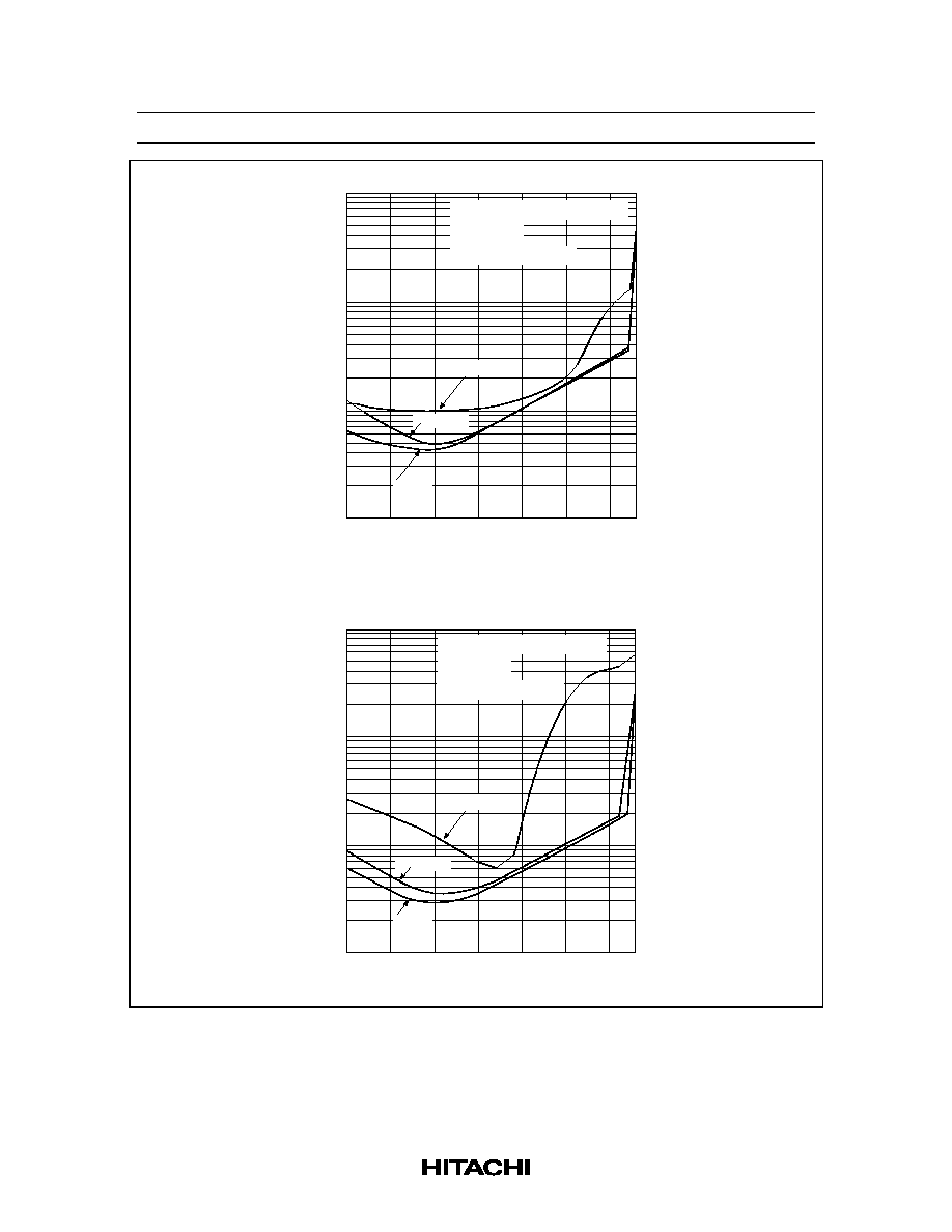
Signal-to-Noise Ratio vs. Supply Voltage (HA12155)
90
80
70
60
50
9
10
11
12
13
14
15
16
Supply voltage Vcc (V)
Signal-to-noise ratio S/N (dB)
E Vol : DAC Step No.18
Vin = 100 mVrms
CCIR/ARM
HA12155NT/HA12157NT
Rev.4, Jun. 1997, page 42 of 57
Signal-to-Noise Ratio vs. Supply Voltage (HA12157)
90
80
70
60
50
10
11
12
13
14
15
16
Supply voltage V (V)
Signal-to-noise ratio S/N (dB)
VRI : DAC Step No.18
Vin = 100 mVrms
CCIR/ARM
PB-C
PB-B
REC-OFF RPI
REC-OFF VRI
RB-OFF
PB-B RPI
REC-B VRI
REC-C RPI
REC-C VRI
CC
Crosstalk vs. Frequency (R L)
Frequency (Hz)
10
100
1 k
10 k
100 k
≠120
≠100
≠80
≠60
≠40
≠20
Crosstalk (R L) (dB)
REC mode RPI in RECOUT out
Vin = +6 dB
V = 14 V
CC
C
B
OFF
HA12155NT/HA12157NT
Rev.4, Jun. 1997, page 43 of 57
Crosstalk vs. Frequency (R L)
Frequency (Hz)
10
100
1 k
10 k
100 k
≠120
≠100
≠80
≠60
≠40
≠20
CC
C
B
Crosstalk (R L) (dB)
OFF
PB mode RPI in PBOUT out
Vin = +6 dB
V = 14 V
Crosstalk (dB)
Crosstalk vs. Frequency
Frequency (Hz)
10
30
60 100
300 600 1 k
3 k 6 k 10 k
30 k 60 k 100 k
≠100
≠80
≠60
≠40
≠20
0
V = 14 V
CC
RPI PBI
RPI VRI
HA12155NT/HA12157NT
Rev.4, Jun. 1997, page 44 of 57
Crosstalk (dB)
Crosstalk vs. Frequency
Frequency (Hz)
10
30
60 100
300 600 1 k
3 k 6 k 10 k
30 k 60 k 100 k
≠100
≠80
≠60
≠40
≠20
0
V = 14 V
CC
PBI RPI
PBI VRI
Crosstalk (dB)
Crosstalk vs. Frequency
Frequency (Hz)
10
30
60 100
300 600 1 k
3 k 6 k 10 k
30 k 60 k 100 k
≠100
≠80
≠60
≠40
≠20
0
V = 14 V
CC
VRI RPI
VRI PBI
HA12155NT/HA12157NT
Rev.4, Jun. 1997, page 45 of 57
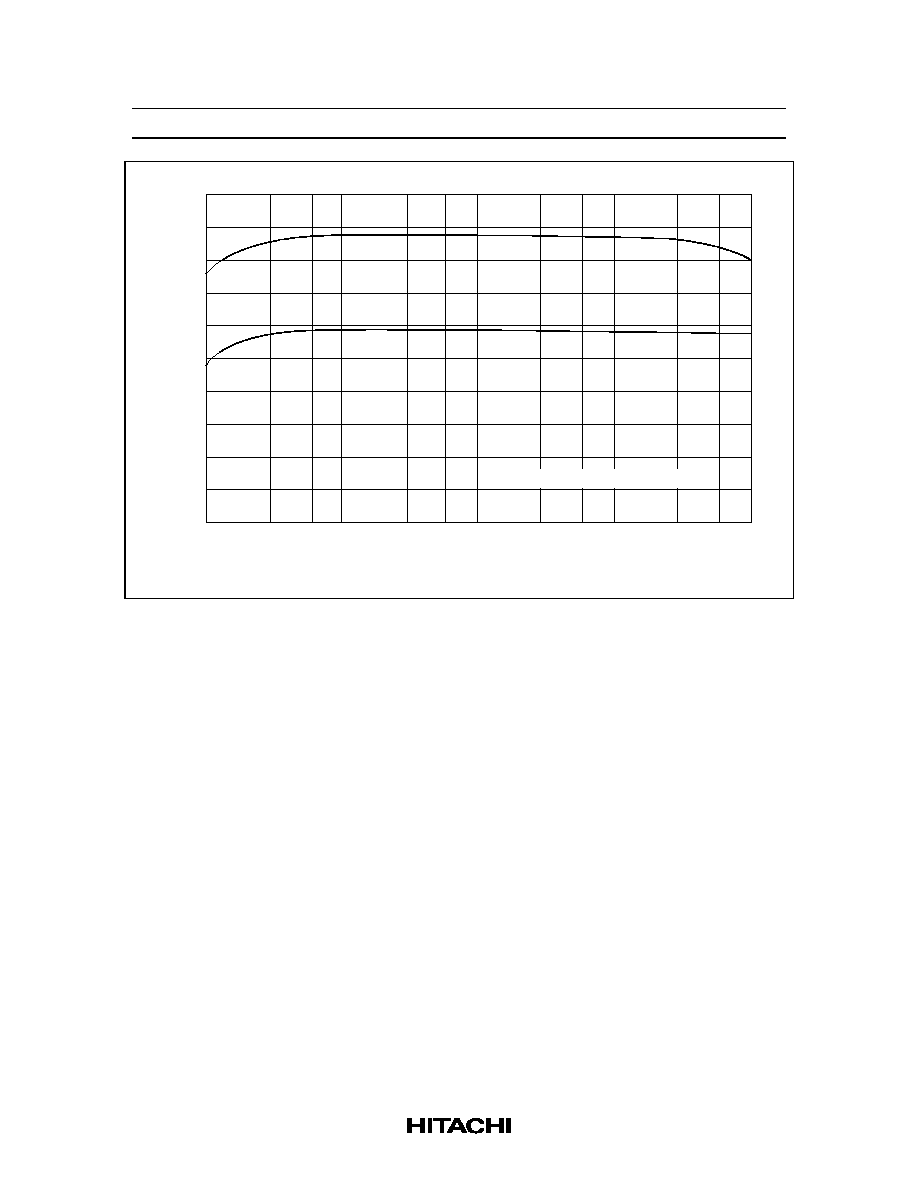
Ripple Rejection Ratio vs. Frequency (REC mode)
Frequency (Hz)
Ripple rejection ratio R.R.R. (dB)
0
≠10
≠20
≠30
≠40
≠50
10
50 100
500 1 k
5 k 10 k
50 k 100 k
V = 14 V RECOUT out
CC
C
B
OFF
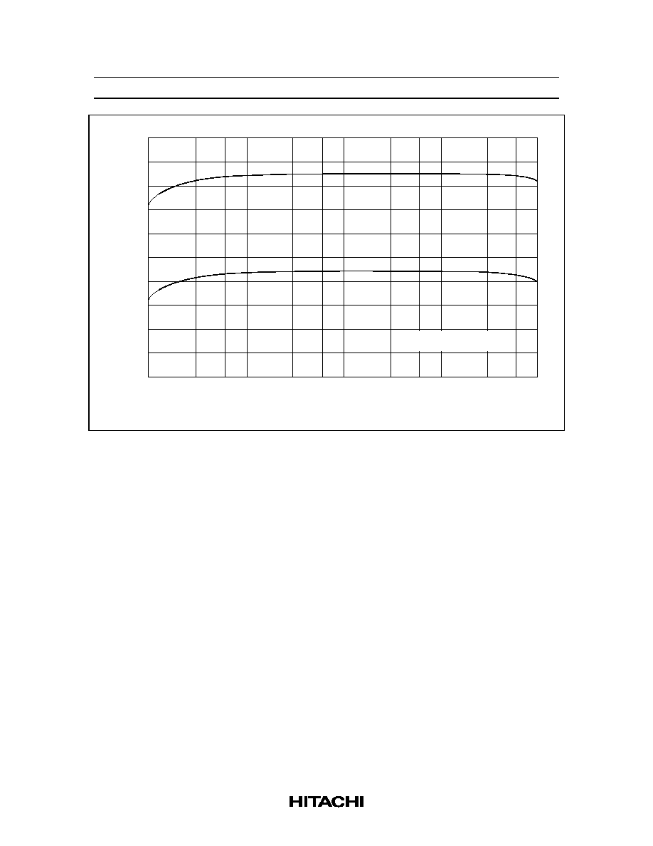
Ripple Rejection Ratio vs. Frequency (PB mode)
Frequency (Hz)
Ripple rejection ratio R.R.R. (dB)
≠10
≠20
≠30
≠40
≠50
≠60
10
50 100
500 1 k
5 k 10 k
50 k 100 k
V = 14 V PBOUT out
CC
B
C
OFF
HA12155NT/HA12157NT
Rev.4, Jun. 1997, page 46 of 57
Gain, S/N and Vomax vs. DAC Step
20
10
0
≠10
≠20
0
20
30
40
10
60
70
80
90
100
DAC Step No.
V = 14 V f = 1 kHz
VRI in IAOUT out
CC
IAOUT gain Gv (dB)
S/N (dB)
Vo max (dB) 0 dB =
≠
5.2 dBs T.H.D. = 1 %
Input level Vin (the value to be converted) (dBs)
20
16
12
8
4
0
2
≠25
≠15
≠5
5
15
≠20
≠10
0
10
S/N
Vo max
Gv.Vin
(JIS A filter)
HA12155NT/HA12157NT
Rev.4, Jun. 1997, page 47 of 57
Total Harmonic Distortion vs. DAC Step
DAC Step
0
10
20
30
40
50
0.01
0.03
0.1
0.3
1.0
3.0
10
Total harmonic distortion T.H.D. (%)
0 dB = ≠5.2 dBs
Vcc = 14 V
f = 100 Hz
IAOUT output level = const
+10 dB
0 dB
≠10 dB
Total Harmonic Distortion vs. DAC Step
DAC Step
0
10
20
30
40
50
0.01
0.03
0.1
0.3
1.0
3.0
10
Total harmonic distortion T.H.D. (%)
0 dB = ≠5.2 dBs
Vcc = 14 V
f = 1 kHz
IAOUT output level = const
+ 10 dB
0 dB
≠ 10 dB
HA12155NT/HA12157NT
Rev.4, Jun. 1997, page 48 of 57
Total Harmonic Distortion vs. DAC Step
DAC Step
0
10
20
30
40
50
0.01
0.03
0.1
0.3
1.0
3.0
10
Total harmonic distortion T.H.D. (%)
0 dB = ≠5.2 dBs
Vcc = 14 V
f = 10 kHz
IAOUT output level = const
+ 10 dB
0 dB
≠ 10 dB
E. Vol Max. Input Level vs. Supply Voltage
16
14
12
10
8
6
4
2
0
8
10
12
14
16
18
Supply voltage V (V)
CC
E. Vol Max. input level Vin max (IAOUT T.H.D. = 1 %) (dB)
f = 1 kHz
IAOUT out DAC Step No.= 42
HA12155NT/HA12157NT
Rev.4, Jun. 1997, page 49 of 57
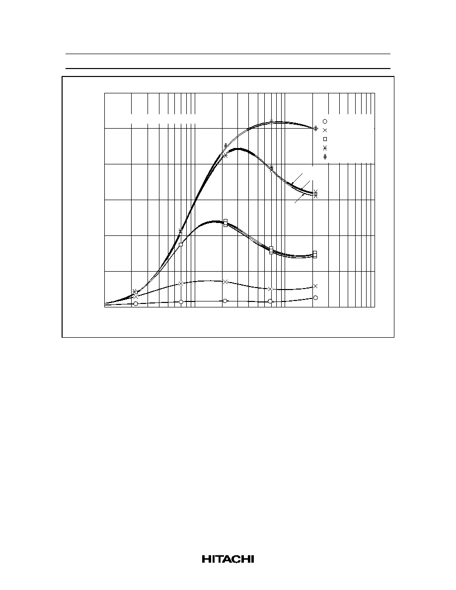
Frequency (Hz)
Electronic Volume Gain vs. Frequency
Electronic volume gain (dB)
10
100
1 k
10 k
100 k
≠70
≠60
≠50
≠10
≠30
≠20
0
10
20
30
≠40
DAC Step0
DAC Step20
DAC Step29
DAC Step36
DAC Step42
DAC Step47
DAC Step51
DAC Step56
DAC Step62
VRI in IAOUT out V = 14 V V in = ≠12 dBs
CC
Level Meter Output vs. Input Level (HA12155)
Input level Vin (dB)
Level meter output (V)
4.0
3.0
2.0
1.0
0
≠80 ≠60 ≠40
≠20
0
20
40
0 dB Range
≠20 dB Range
0 dB = 580 mVrms
V = 14 V
f = 1 kHz
CC
HA12155NT/HA12157NT
Rev.4, Jun. 1997, page 50 of 57
Level Meter Output vs. Input Level (HA12157)
Input level Vin (dB)
Level meter output (V)
4.0
3.0
2.0
1.0
0
≠80 ≠60 ≠40
≠20
0
20
40
0 dB Range
≠20 dB Range
0 dB = 775 mVrms
V = 14 V
f = 1 kHz
CC
Level Meter Output vs. Frequency
Frequency (Hz)
Level meter output (V)
3.2
3.0
2.8
2.6
2.4
2.2
2.0
20 30
100
300
1 k
3 k
10 k
30 k
100 k
V = 14 V
CC
0 dB Range Vin = 0 dB
≠20 dB Range Vin = ≠20 dB
HA12155NT/HA12157NT
Rev.4, Jun. 1997, page 51 of 57
Level Meter Output vs. Supply Voltage
4.0
3.0
2.0
1.0
0
8
10
12
14
16
18
0 dB Range Vin = 0 dB
≠20 dB Range Vin = ≠20 dB
Supply voltage V (V)
CC
Level meter output (V)
f = 1 kHz
0 dB Range Vin = ≠20 dB
0 dB Range Vin = 12 dB
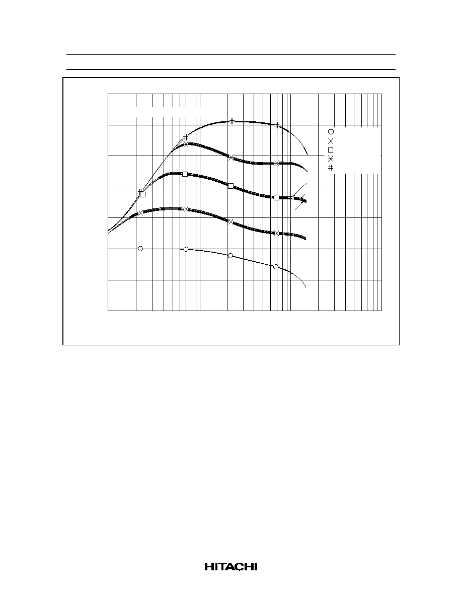
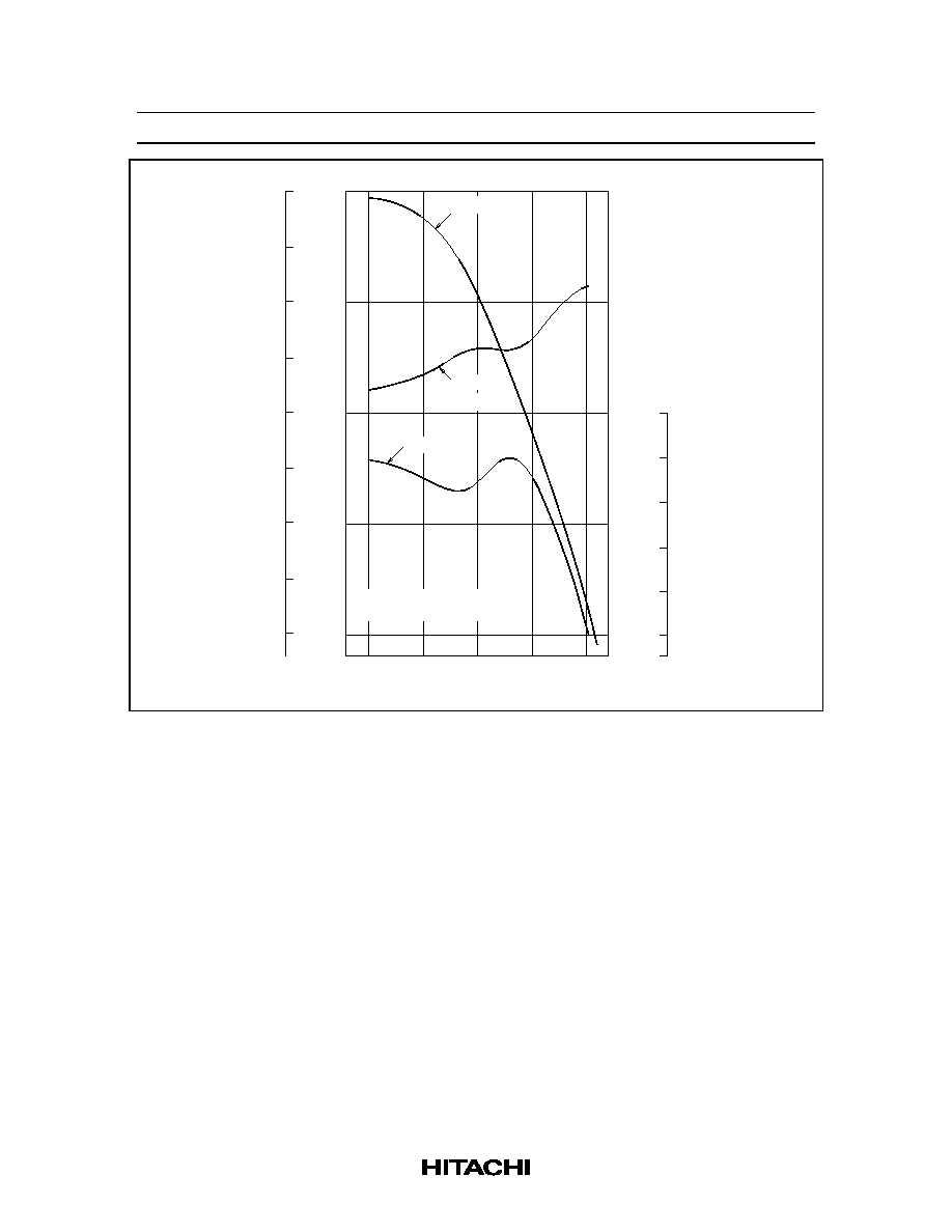
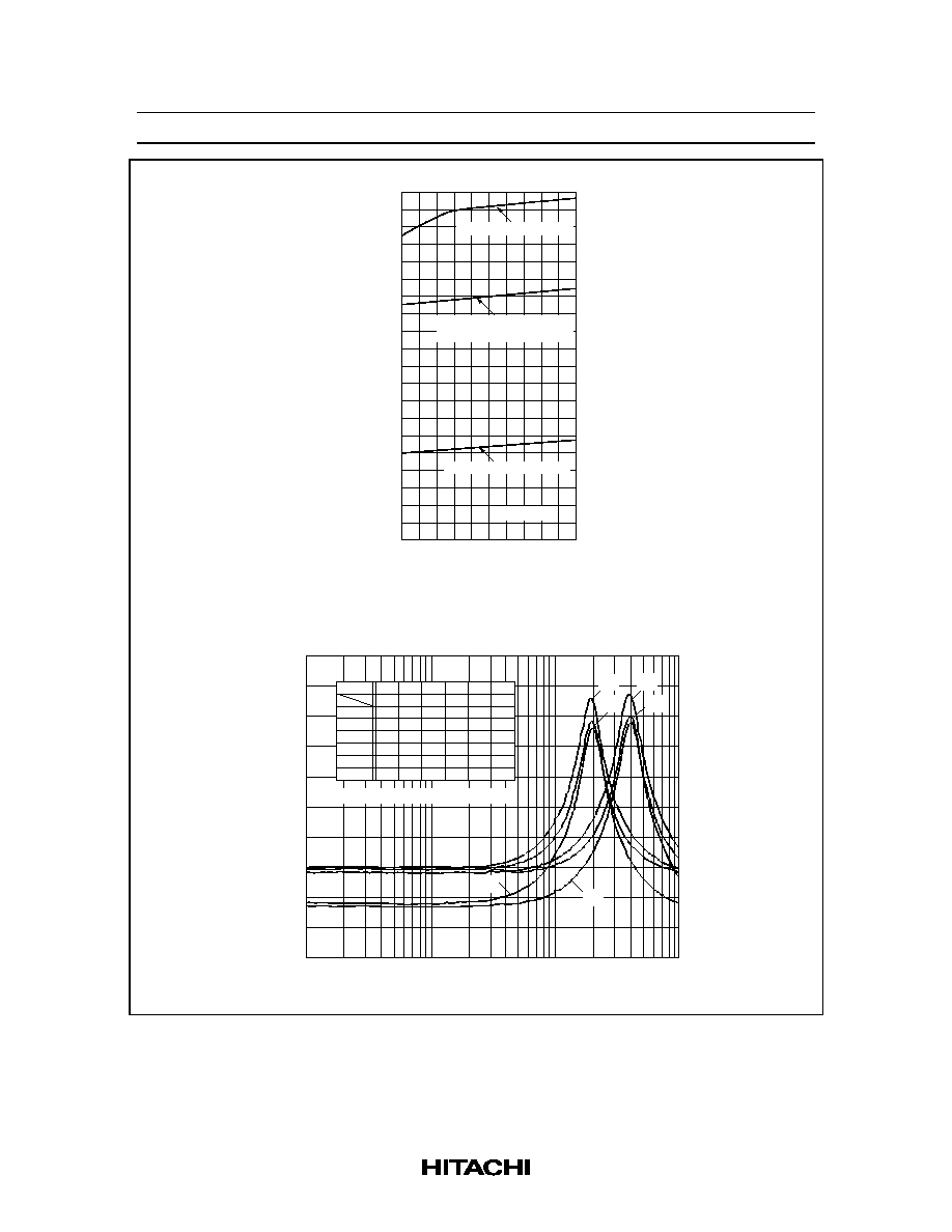
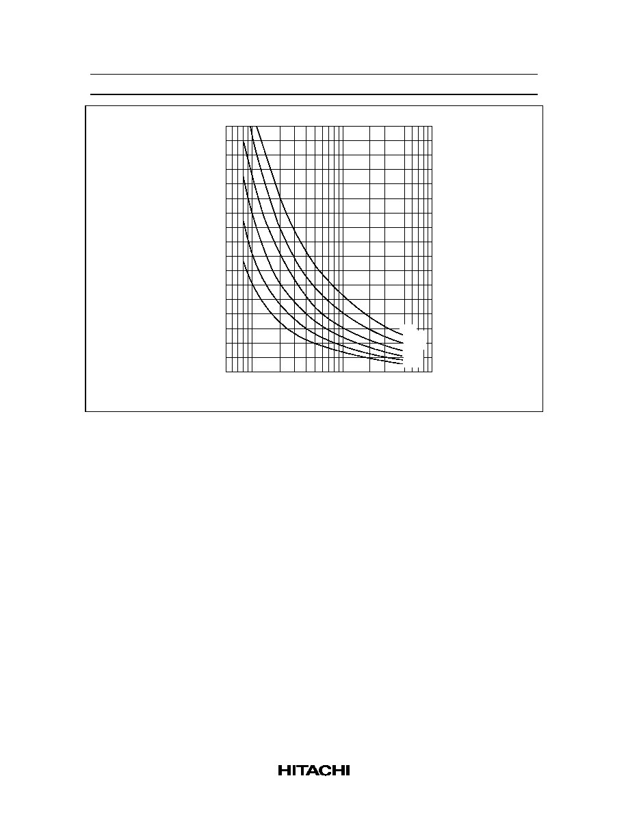
Equalizer Gain vs. Frequency
Frequency (Hz)
Equalizer gain (dB)
40
25
10
1 k
300
10
3 k
10 k
30 k
100 k
(5)
(3)
(6)
(4)
(1)
(2)
R
GP
R
GL
R
GH
R
F/Q
R
FQ
R
FM
(1) (2) (3) (4)
(5) (6)
NN HN NC HC NM HM
33 k
33 k
33 k
51 k
51 k
100 k100 k 100 k100 k100 k100 k
33 k 33 k 33 k 47 k 47 k
33 k 51 k 51 k 51 k 51 k
33 k
51 k 20 k 51 k 20 k
27 k 51 k 27 k 51 k 27 k
51 k 51 k 51 k 51 k
V = 14 V Vin = ≠20 dBs
CC
20 k
HA12155NT/HA12157NT
Rev.4, Jun. 1997, page 52 of 57
Output level Vout (dB)
Total hrmonic distortion T.H.D. (%)
Equalizer Total Harmonic Distortion vs. Output Level
≠10
≠5
0
5
10
15
20
0.1
0.3
1.0
3.0
10
30
V = 14 V
0 dB = ≠5 dBs
Rload = 10 k
R = 33 k
R = 33 k
R = 100 k
R = 33 k
R = 51 k
R = 51 k
CC
GL
GH
FM
GP
F/Q
FQ
: 15 kHz
: 10 kHz
: 6.3 kHz
: 3.15 kHz
: 1 kHz
: 315 Hz
35
30
25
20
15
10
5
5k 10 k
30 k
100 k
1 M
300 k
Equalizer Amplifier Gain (GL) vs. R
R ( )
Equalizer amplifier gain GL (dB)
at R = 33 k
V out = –5 dBs
GP
F/Q
f = 315 Hz
f = 1 kHz
V = 14V
R = R = 33 k
R = R = 51 k
R = 100 k
CC
GH
FQ
FM
GL
GL
GL
HA12155NT/HA12157NT
Rev.4, Jun. 1997, page 53 of 57
Equalizer Amplifier Gain (GH) vs. R
GH
35
30
25
20
15
10
5
5k 10 k
30 k
100 k
1 M
300 k
R ( )
Equalizer amplifier gain GH (dB)
GH
at R = 33 k
Vout = –5 dBs
GH
CC
GL
GP
FQ
FM
F/Q
V = 14 V
R = 33 k
R = 16 k
R = R = 24 k
R = 390 k
f = 6.3 kHz
Equalizer Amplifier Gain (GP) vs. R
GP
50
45
40
35
30
25
20
5k 10 k
30 k
100 k
1 M
300 k
R ( )
Equalizer amplifier gain GP (dB)
GP
CC
GH
GP
F/Q
FQ
FM
V = 14 V
R = R = 33 k
R = R = 51 k
R = 100 k
f = 19 kHz
HA12155NT/HA12157NT
Rev.4, Jun. 1997, page 54 of 57
Equalizer Cut off Frequency (FM) vs. R
FM
100 k
30 k
10 k
3 k
1 k
300
5 k
10 k
30 k
100 k
300 k
1 M
R ( )
FM
Equalizer cut off frequency FM (Hz)
V = 14 V
R = 120 k
R = 7.5 k
R = R = 24 k
R = 16 k
CC
GL
GH
FQ
GP
F/Q
Equalizer Peak Frequency vs. R
FQ
300 k
100 k
30 k
10 k
3 k
2 k
5 k
10 k
30 k
100 k
300 k
1 M
R ( )
FQ
Equalizer peak frequency fo (Hz)
R =
F/Q
12 k
24 k
51 k
100 k
200 k
390 k
HA12155NT/HA12157NT
Rev.4, Jun. 1997, page 55 of 57
Equalizer Q vs. R
FQ
15
10
5
0
5 k
10 k
30 k
100 k
300 k
1 M
R ( )
FQ
Equalizer quality factor Q
R =
390 k
200 k
100 k
51 k
24 k
12 k
F/Q
HA12155NT/HA12157NT
Rev.4, Jun. 1997, page 56 of 57
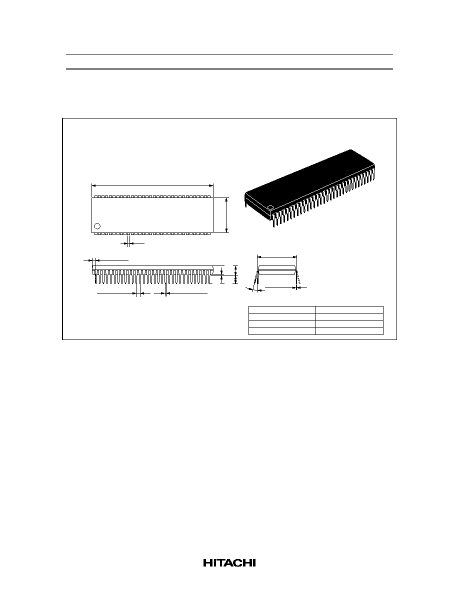
Package Dimensions
Unit: mm
0.25
+ 0.11
≠ 0.05
0∞ ≠ 15∞
1.78 ± 0.25
0.48 ± 0.10
0.51 Min
2.54 Min
5.08 Max
19.05
57.6
58.5 Max
1.0
1
33
32
64
17.0
18.6 Max
1.46 Max
Hitachi Code
JEDEC Code
EIAJ Code
Weight
DP-64S
--
SC-553-64A
8.8 g

HA12155NT/HA12157NT
Rev.4, Jun. 1997, page 57 of 57
Disclaimer
1. Hitachi neither warrants nor grants licenses of any rights of Hitachi's or any third party's patent,
copyright, trademark, or other intellectual property rights for information contained in this document.
Hitachi bears no responsibility for problems that may arise with third party's rights, including
intellectual property rights, in connection with use of the information contained in this document.
2. Products and product specifications may be subject to change without notice. Confirm that you have
received the latest product standards or specifications before final design, purchase or use.
3. Hitachi makes every attempt to ensure that its products are of high quality and reliability. However,
contact Hitachi's sales office before using the product in an application that demands especially high
quality and reliability or where its failure or malfunction may directly threaten human life or cause risk
of bodily injury, such as aerospace, aeronautics, nuclear power, combustion control, transportation,
traffic, safety equipment or medical equipment for life support.
4. Design your application so that the product is used within the ranges guaranteed by Hitachi particularly
for maximum rating, operating supply voltage range, heat radiation characteristics, installation
conditions and other characteristics. Hitachi bears no responsibility for failure or damage when used
beyond the guaranteed ranges. Even within the guaranteed ranges, consider normally foreseeable
failure rates or failure modes in semiconductor devices and employ systemic measures such as fail-
safes, so that the equipment incorporating Hitachi product does not cause bodily injury, fire or other
consequential damage due to operation of the Hitachi product.
5. This product is not designed to be radiation resistant.
6. No one is permitted to reproduce or duplicate, in any form, the whole or part of this document without
written approval from Hitachi.
7. Contact Hitachi's sales office for any questions regarding this document or Hitachi semiconductor
products.
Sales Offices
Hitachi, Ltd.
Semiconductor & Integrated Circuits.
Nippon Bldg., 2-6-2, Ohte-machi, Chiyoda-ku, Tokyo 100-0004, Japan
Tel: Tokyo (03) 3270-2111 Fax: (03) 3270-5109
Copyright
Hitachi, Ltd., 2000. All rights reserved. Printed in Japan.
Hitachi Asia Ltd.
Hitachi Tower
16 Collyer Quay #20-00,
Singapore 049318
Tel : <65>-538-6533/538-8577
Fax : <65>-538-6933/538-3877
URL : http://www.hitachi.com.sg
URL
NorthAmerica
: http://semiconductor.hitachi.com/
Europe
: http://www.hitachi-eu.com/hel/ecg
Asia
: http://sicapac.hitachi-asia.com
Japan
: http://www.hitachi.co.jp/Sicd/indx.htm
Hitachi Asia Ltd.
(Taipei Branch Office)
4/F, No. 167, Tun Hwa North Road,
Hung-Kuo Building,
Taipei (105), Taiwan
Tel : <886>-(2)-2718-3666
Fax : <886>-(2)-2718-8180
Telex : 23222 HAS-TP
URL : http://www.hitachi.com.tw
Hitachi Asia (Hong Kong) Ltd.
Group III (Electronic Components)
7/F., North Tower,
World Finance Centre,
Harbour City, Canton Road
Tsim Sha Tsui, Kowloon,
Hong Kong
Tel : <852>-(2)-735-9218
Fax : <852>-(2)-730-0281
URL : http://www.hitachi.com.hk
Hitachi Europe Ltd.
Electronic Components Group.
Whitebrook Park
Lower Cookham Road
Maidenhead
Berkshire SL6 8YA, United Kingdom
Tel: <44> (1628) 585000
Fax: <44> (1628) 585160
Hitachi Europe GmbH
Electronic Components Group
Dornacher Straþe 3
D-85622 Feldkirchen, Munich
Germany
Tel: <49> (89) 9 9180-0
Fax: <49> (89) 9 29 30 00
Hitachi Semiconductor
(America) Inc.
179 East Tasman Drive,
San Jose,CA 95134
Tel: <1> (408) 433-1990
Fax: <1>(408) 433-0223
For further information write to:
Colophon 2.0